Laser-slicing of silicon with 3D nonlinear laser
lithography
Onur Tokel1,2, Ahmet Turnali1, Tahir C¸olako˘glu3, Serim Ilday,2, Mona Zolfaghari
Borra3, Ihor Pavlov1,2, Alpan Bek3, Ras¸it Turan3, and F. ¨Omer Ilday1,2
1Department of Electrical and Electronics Engineering, Bilkent University, Ankara, 06800, Turkey 2Department of Physics, Bilkent University, Ankara, 06800, Turkey
3Department of Physics, Middle East Techical University, Ankara, 06800 ,Turkey
Abstract: Recently, we have showed a direct laser writing method that exploits nonlinear interactions to form subsurface modifications in silicon. Here, we use the technique to demonstrate laser-slicing of silicon and its applications.
OCIS codes: 140.3390, 230.0230, 230.0220
Conventional lithography techniques work successfully in fabricating functional elements on Si. However, these methods cannot be used to fabricate devices inside Si without damaging the surface. Recently, we reported a technique, which accomplishes single-step, maskless laser writing deep inside Si, and can be used to create highly-controllable modifications inside Si, without damaging the surface [1]. The developed method exploits the nonlinear interactions [2] of laser in Si. Using this approach, we demonstrated the first optical elements buried deep inside silicon [3]. Here, we use our method for laser-slicing of Si and present relevant applications. Laser-slicing of Si is appealing because removing mechanical dicing steps is desired to avoid damages around cut regions. Further, the high refractive index contrast between Si and air is ideal for creating optical elements, such as photonic crystals, or potentially anti-reflective surfaces.
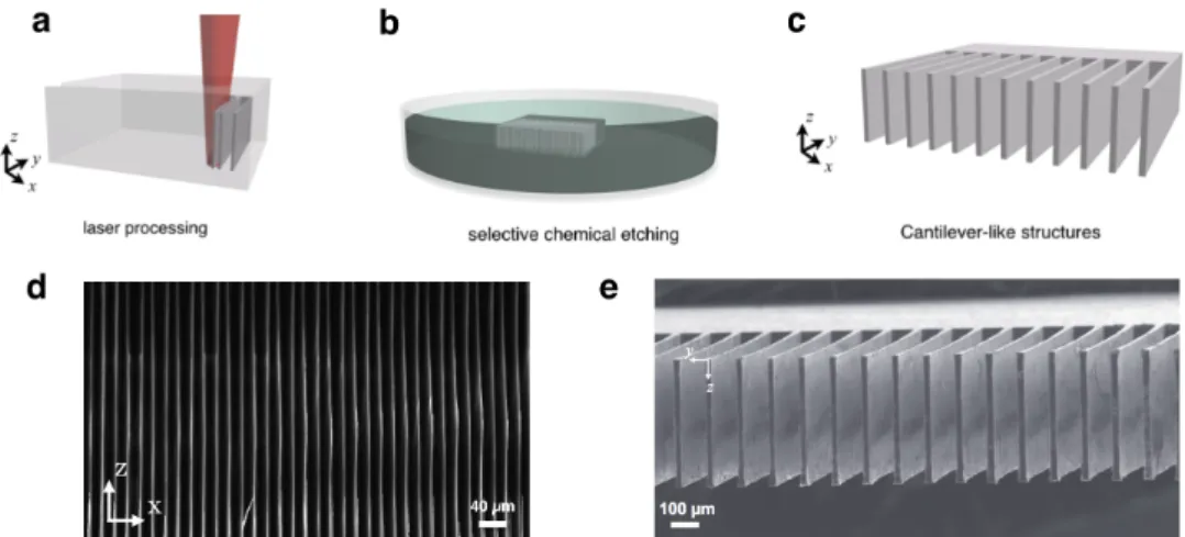
Fig. 1 (a) The laser is used to create controllable structures deep inside Si. (b) The processed volume is selectively etched. (c) Exposed 3D architecture. (d) SEM image of final 3D architecture. (e) SEM image shows a 3D array in Si.
We used a home-built, all-fibre master oscillator power amplifier (MOPA) system that produces 5-ns pulses and operates at 1.55µm. First, 3D structures were laser written inside Si (Figs. 1a). Then, a selective etching is used to expose the unprocessed Si (Figs. 1b-1c). The method allows to produce micropillar arrays, microchannels, and cantilever-like structures among others. For instance, Fig. 1d shows thin slices of Si, and Fig. 1e shows high-aspect-ratio walls. The method is rapid, inexpensive, maskless and can be easily scalable. In conclusion, laser-slicing of silicon is demonstrated. The high-aspect-ratio, controllable structures and the resulting slicing capability are notable for being the first examples of subsurface laser slicing of Si without mechanical dicing. References
1. O. Tokel, A. Turnali, I. Pavlov, F. ¨Omer Ilday , ”Laser writing deep inside silicon for 3D information processing,” presented at CLEO/EU-EQEC, Munich, Germany, 21–25 June 2015.
2. B. ¨Oktem, I. Pavlov, S. Ilday, H. Kalaycıo˘glu, A. Rybak, S. Yavas¸, M. Erdo˘gan, F. ¨O. Ilday, ”Nonlinear laser lithography for indefinitely large-area nanostructuring with femtosecond pulses”, Nat. Photon.7, 897 (2013)
3. A. Turnali, O. Tokel, I. Pavlov, F. ¨Omer Ilday , ”Direct laser writing of volume fresnel zone plates in silicon,” presented at CLEO/EU-EQEC, Munich, Germany, 21–25 June 2015.