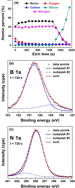
Low-Temperature Deposition of Hexagonal Boron Nitride via Sequential Injection of Triethylboron and N2/H2 Plasma
Tam metin
Şekil


Benzer Belgeler
In particular, we will derive the expressions for the expected cycle length, expected inventory-days (i.e., inventory carried over time) after the lead time period and the
The risk metric introduced below estimates the size of the expected population that resides within a given radius of the location of a train accident involving a release of
In this study, therefore, we attended to core and peripheral beliefs, examined the influence of language teachers’ contexts on their work and elicited beliefs through the analysis
A total of 120 interior architecture students were sur- veyed about their experiences on five fields of instruction: (1) course design, learning material and electronic
Hypothesis states that export expansion in manufacturing industry can be explained by export subsidies, real effective exchange rate, labor wages and capacity
export growth, as was the case in South Korea, Hong Kong, Singapore, and Taiwan ; (2) Turkey has a large population composed of mostly unskilled labor
It is explicitly shown with several examples that Godel-type metrics can be used in obtaining exact solutions to¨ various supergravity theories and in constructing spacetimes
How- ever, when both the homo and copolymers of PEI with larger molecular weights (PEIs with 25 kDa molecular weight) either linear (L) or branched (B) were used, the plasmid DNA
