Solar-blind AlxGa1−xN-based avalanche photodiodes
Turgut Tut, Serkan Butun, Bayram Butun, Mutlu Gokkavas, HongBo Yu et al.
Citation: Appl. Phys. Lett. 87, 223502 (2005); doi: 10.1063/1.2135952
View online: http://dx.doi.org/10.1063/1.2135952
View Table of Contents: http://apl.aip.org/resource/1/APPLAB/v87/i22
Published by the American Institute of Physics.
Additional information on Appl. Phys. Lett.
Journal Homepage: http://apl.aip.org/
Journal Information: http://apl.aip.org/about/about_the_journal
Top downloads: http://apl.aip.org/features/most_downloaded
Information for Authors: http://apl.aip.org/authors
Solar-blind Al
xGa
1−xN-based avalanche photodiodes
Turgut Tut, Serkan Butun, Bayram Butun, Mutlu Gokkavas, HongBo Yu, and Ekmel Ozbay
Nanotechnology Research Center, Bilkent University, Bilkent, 06800 Ankara, Turkey
共Received 11 October 2005; accepted 18 October 2005; published online 21 November 2005兲 We report the Metalorganic Chemical Vapor Deposition 共MOCVD兲 growth, fabrication, and characterization of solar blind AlxGa1−xN / GaN-based avalanche photodiodes. The photocurrent
voltage characteristics indicate a reproducible avalanche gain higher than 25 at a 72 V applied reverse bias. Under a 25 V reverse bias voltage, the 100 m diameter devices had a maximum quantum efficiency of 55% and a peak responsivity of 0.11 A / W at 254 nm, and a NEP of 1.89x10⁻¹⁶W / Hz1/2. © 2005 American Institute of Physics.关DOI:10.1063/1.2135952兴
The recent developments in GaN / AlGaN material growth technology have led to the fabrication of high perfor-mance photodetectors operating in the UV spectral region. AlGaN-based Schottky,1,2p-i-n3,4and MSM5photodetectors with excellent detectivity performances have been reported. However, very few GaN-based avalanche photodiodes 共APDs兲 were reported in the literature,6–11
and there are not any publications reporting AlGaN-based APDs. The high de-fect densities in the epitaxial layers grown on lattice-mismatched substrates result in a premature microplasma breakdown before the electric field can reach the bulk ava-lanche breakdown level, which is a major problem for the AlGaN / GaN APDs.8,11In this paper, we report the epitaxial growth, fabrication, and characterization of AlGaN-based APDs operating in the solar-blind spectral region.
The epitaxial structure of the front-illumination Schottky detector wafer was designed to achieve true-solar blindness, very low dark current, high solar rejection, and high break-down. Low leakage and high breakdown are needed in order to see the avalanche effect. The Al0.38Ga0.62N absorption
layer was used to achievec⬍280 nm. The AlxGa1−xN / GaN
epitaxial layers of our heterojunction Schottky photodiode wafer were grown on a 2 in. single-side polished 共0001兲 sapphire substrate using the Aixtron 200/ 4 RF-S MOCVD system located at the Bilkent University Nanotechnology Re-search Center. A thin AlN nucleation layer and a subsequent 0.5m thick unintentionally doped GaN mesa isolation layer was first grown. This was followed by the growth of a highly doped 共n+= 2⫻1018 cm−3兲0.6m thick GaN Ohmic contact layer and a 0.2m thick Al0.38Ga0.62N layer at the
same doping level. The epitaxial growth of the wafer was completed with the deposition of a 0.8m thick undoped Al0.38Ga0.62N active layer. The highly doped GaN layer was used for the Ohmic contact region due to the difficulty of obtaining high-quality Ohmic contacts with AlxGa1−xN
lay-ers. The n-type doped 0.2m thick Al0.38Ga0.62N layer was
used as a diffusion barrier for the photocarriers generated in the GaN Ohmic contact layer. Such a diffusion barrier is expected to increase the solar-blind/near-UV rejection ratio of the detector.
The samples were fabricated by using a five-step microwave-compatible fabrication process in a class-100 clean room environment. First, the Ohmic contact regions were defined via reactive ion etching 共RIE兲 under CCl2F2
plasma, a 20 sccm gas flow rate, and 100W rf power. The etch rates for the GaN and Al0.38Ga0.62N layers were 326 and
178 Å / min., respectively. After an Ohmic etch of
⬃1.2m , Ti/ Al共100 Å/1000 Å兲 contacts were deposited via thermal evaporation and left in an acetone solution for the lift-off process. The contacts were annealed at 650 °C for 60 s in a rapid thermal annealing system. A⬃100 Å thick Au film was evaporated in order to form Au/ AlGaN Schottky contacts. Mesa structures of the devices were formed via the same RIE process, by etching all of the layers 共⬎2.1m兲 down to the sapphire substrate layer for better mesa isola-tion. Then, a 200 nm thick Si3N4was deposited via
plasma-enhanced chemical vapor deposition共PECVD兲 for passiva-tion. Finally, a⬃0.6 m thick Ti/ Au interconnect metal was deposited and lifted off to connect the Schottky layers to the coplanar waveguide transmission line pads.
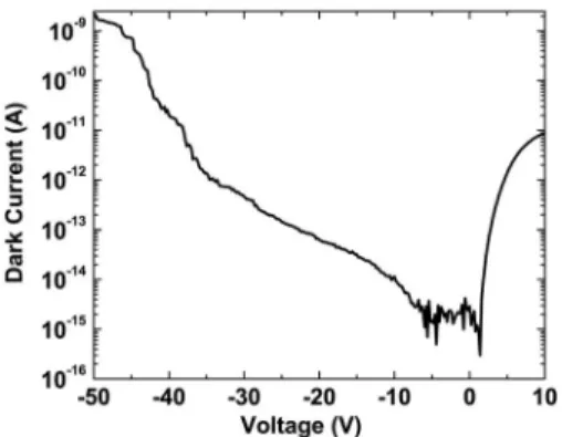
The resulting devices had breakdown voltages higher than 50 V. To obtain better isolation, we etched down to the sapphire substrate, which enabled us to obtain lower leakage current than previous fabrications. Figure 1 shows the dark current of a 60m diameter device. Dark current density at a 5 V reverse bias was 5.3⫻10−11A / cm2. Up to 10 V, the
dark current was less than 10 fA. At 50 V bias, the device had a dark current ⬃2 nA. The low dark current values proved the high growth quality of an AlGaN wafer with low dislocation densities. The differential resistance of our detec-tors at zero bias was in excess of 1.88⫻1015⍀ in the 0–20
V range.
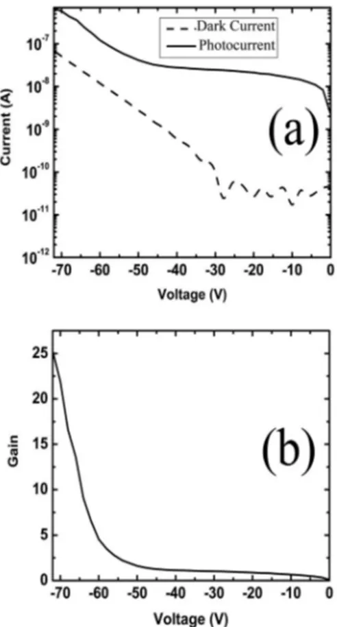
Figure 2共a兲 shows the current-voltage characteristics of a device with a 100m diameter. The device showed almost unity-gain behavior for voltages between 10 and 50 V, and the photocurrent was approximately 10 nA. After 50 V, ava-lanche gain has been observed from the device. As shown in Fig. 2共b兲, the maximum reproducible avalanche gain was 25 at 72 V reverse bias. The onset avalanche gain field was
FIG. 1. Dark current of a 60m diameter photodetector.
APPLIED PHYSICS LETTERS 87, 223502共2005兲
0003-6951/2005/87共22兲/223502/3/$22.50 87, 223502-1 © 2005 American Institute of Physics
estimated to be approximately 1 MV/ cm. Although we had observed avalanche gains as high as 200共at ⬃85 V reverse bias兲 from some of the devices, the performance of these devices degraded rapidly after the measurements.
Figure 3共a兲 shows the quantum efficiency measurements of a 100m diameter device for different bias voltages.
Un-der a 25 V reverse bias voltage, the device had a maximum quantum efficiency of 55% at 254 nm. The cut off wave-length was ⬃270 nm for all measurements. Figure 3共b兲 shows the responsivity measurements of the same photode-tector. The peak responsivity was 0.11 A / W at a wavelength of 254 nm. The device had a rejection ratio of more than four orders of magnitude with wavelengths larger than 362 nm at a 25 V reverse bias. Using the thermal-noise-limited detec-tivity共D*兲 formula D*= R共R0A / 4kT兲1/2, where Ris the
de-vice responsivity at zero bias, R0is the zero volt dark
imped-ance, and A is the detector area, D* is found as 4.68
⫻1013cm Hz1/2/ W, which is higher than our earlier results.2
The corresponding noise-equivalent power 共NEP兲 is 1.89 ⫻10−16W / Hz1/2.
Finally, the noise characterization of the solar-blind de-tectors was carried out using a fast Fourier transform spec-trum analyzer, current amplifier, dc voltage source, and a microwave probe station. In the 1 Hz–10 kHz range, our low-leakage, high breakdown voltage solar-blind photodetec-tors had noise power densities below the resolution level of the instrument. Even under 30 V, the detector noise did not exceed the measurement setup noise floor of 3 ⫻10−29A2/ Hz at 10 kHz. Therefore, we measured devices
with higher leakage currents in order to observe the bias dependence of the spectral noise density. We took a 100m diameter device that has higher dark current 共5⫻10−7A at 35 V兲 and a lower breakdown voltage near 50 V. As can be seen in Fig. 4, 1 / f 共flicker兲 noise is the dominant noise mechanism in our detectors. 1 / f noise is known to result from contamination and crystal imperfection. Up to 30 V reverse bias voltage, the noise power density is nearly the same. At a 0 V bias voltage and 10 Hz, Sn共f兲 is ⬃9.8
⫻10−21A2/ Hz, at 30 V bias it is only ⬃3⫻10−20A2/ Hz,
and at 50 V it is⬃1.4⫻10−16A2/ Hz. The noise curves obey
the Sn= S0/ fbrelation. S0 depends on current, which is why
the noise increases with an applied bias voltage in low frequencies.
In summary, we report the first solar-blind AlGaN-based avalanche photodiodes with low dark current, low noise, and high detectivity. The photocurrent-voltage characteristics in-dicated a reproducible gain of ⬎25 at 72 V. The devices exhibited a maximum quantum efficiency of 55% and a peak responsivity of 0.11 A / W at a wavelength of 254 nm.
1A. Osinsky, S. Gangopadhyay, B. W. Lim, M. Z. Anwar, M. A. Khan,
D. V. Kuksenkov, and H. Temkin, Appl. Phys. Lett. 72, 742共1998兲.
2T. Tut, N. Biyikli, I. Kimukin, T. Kartaloglu, O. Aytur, M. S. Unlu,
and E. Ozbay, Solid-State Electron. 49, 117共2005兲.
3U. Chowdhury, M. M. Wong, C. J. Collins, B. Yang, J. C. Denyszyn,
J. C. Campbell, and D. Dupuis, J. Cryst. Growth 248, 552共2003兲. FIG. 2. 共a兲 Dark current and photocurrent measurement of a 100 micron
diameter photodetector. 共b兲 Corresponding avalanche gain of the same device.
FIG. 3.共a兲 Quantum efficiency measurements of a 100m diameter pho-todetector.共b兲 Responsivity measurement of the same device in a semilog scale.
FIG. 4. Spectral noise measurement of a high-leakage 100m diameter photodetector with a varying applied reverse bias.
223502-2 Tut et al. Appl. Phys. Lett. 87, 223502共2005兲
4N. Biyikli, I. Kimukin, O. Aytur, E. Ozbay, IEEE Photon. Technol. Lett. 16, 1718共2004兲.
5T. Li, D. J. H. Lambert, A. L. Beck, C. J. Collins, B. Yang, J. M. M. Wong,
U. Chowdhury, R.D. Dupuis and J. C. Campbell, Electron. Lett. 36, 1581 共2000兲.
6K. A. McIntosh, R. J. Molnar, L. J. Mahoney, A. Lightfoot, M. W. Geis,
K. M. Molvar, I. Melngailis, R. L. Aggarwal, W. D. Goodhue, S. S. Choi, D.L. Spears, and S. Verghese, Appl. Phys. Lett. 75, 3485共1999兲.
7J. C. Carrano, D. J. H. Lambert, C. J. Eiting, C. J. Collins, T. Li, S. Wang,
B. Yang, A. L. Beck, R. D. Dupuis, and J. C. Campbell, Appl. Phys. Lett.
76, 924共2000兲.
8A. Osinsky, M. S. Shur, R. Gaska, and, Q. Chen, Electron. Lett. 34, 691
共1998兲.
9S. Verghese, K. A. McIntosh, R. J. Molnar, L. J. Mahoney,
R. L. Aggarwal, M. W. Geis, K. M. Molvar, E. K. Duerr, and I. Melngailis, IEEE Electron Device Lett. 48, 502共2001兲.
10K. A. McIntosh, R. J. Molnar, L. J. Mahoney, K. M. Molvar, N. Efremov,
and S. Verghese, Appl. Phys. Lett. 76, 3938共2000兲.
11B. Yang, T. Li, K. Heng, C. Collins, S. Wang, J. C. Carrano, R. D. Dupuis,
J. C. Campbell, M. J. Schurman, and I. T. Ferguson, IEEE J. Quantum Electron. 36, 1389共2000兲.
223502-3 Tut et al. Appl. Phys. Lett. 87, 223502共2005兲