Mehdi F ARDMANESH
Electrical and Electronics Engineering Dept., Bilkent University, 06800 Ankara, Turkey
1. INTRODUCTION
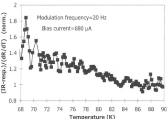
One of the pronusmg devices made of high temperature superconducting (HTSC) materials are edge transition bolometers. Since the discovery of high-temperature superconductors, many works have been focused on the application of these materials in different types of bolometers for the near to far infrared wavelength regime [1]-[9]. They can be used to detect electromagnetic radiation over the whole spectrum from x-ray to the far-infrared (lJ, [9J-[13J. The superconductor bolometers typically consist of patterned thin or thick superconducting films deposited on crystalline substrates such as MgO, SrTi03, and LaAl03 . Their operation is based upon their steep drop in the resistance, R, at their transition temperature, T c. The detector is typically held at a temperature close to the middle of the superconducting transition, where the dRldT is maximum. When the detector is illuminated its temperature rises by an amount proportional to the input radiation power resulting in a ~R. The response obtained by the above mechanism is the so called the bolometric, or equilibrium response, as opposed to typically faster non-bolometric or intrinsic response caused by other mechanisms such as direct depairing. A typical response of an YBCO sample versus temperature at low frequencies is shown in Figure 1. 1.
The responsivity versus modulation frequency and versus the temperature of edge-transition superconductive bolometers has been investigated and reported in different works [7]-[9], [14]-[18]. For example by use ofa dc bias current the change in the resistance of the edge transition bolometer due to the absorbed radiation power can be measured. The detected signal obtained by this biasing can be bolometric, non-bolometric or a combination of both. Since the fabrication and testing of the first detectors, there have been many debates on the mechanism of the response in these devices. This is while the response at low frequencies of superconductor edge transition bolometer is commonly agreed to be mainly bolometric. But there have also been reports that the low frequency response of some samples is also enhanced strongly by an intrinsic response [19]-[21]. This has been reported to be dependent on bias
A. V. Narlikar (ed.), High Temperature Superconductivity 2 © Springer-Verlag Berlin Heidelberg 2004
t- 1.0
~
~ 0.8..
i
0.6f
I
l\
- - Magnitude dRJdT - - Resistance ~ 0.4 'C.,
N1
0.2 0 z 0.0 88 89 90 91 92 93 94 95 96 Temperature (K)Figure L L Normalized resistance and magnitude of the response at 20 Hz vs. temperature of 20l-lmx 100l-lm area and 51-lm wide meander line pattern on 1 mm thick LaAI03 substrate.
cUlTent, radiation, and temperature [19]-[21]. The interpretation and the analysis of the above is strongly dependent on the thermal properties of the substrate and its dimensions, the superconducting pattern, the modulation frequency regime with respect to the effective thermal diffusion length into the substrate, and electrical and the thermal operating conditions of the detectors [7], [18].
Major effects of the substrate-holder and substrate-film thermal boundary resistance on the response of this kind of bolometers are also reported [7], [9], [14]-[18]. For superconductive edge-transition bolometers with flat crystalline substrates directly in contact with the cold-finger, the effects of limited dc thermal conductance, G(O), and louie heating on the response of the detectors have been misleading factor, resulting in unrealistic values for responsivities and detectivities [22]-[23]. This is particularly so for the low and midrange modulation frequency response of detectors with large area superconductive meander line patterns on crystalline substrates such as MgO, LaAI03, and SrTi03 [7], [24] . The above effects are strongly dependent on the dimensions of the pattern of the superconducting film with respect to that of the substrate, and the electrical connections [25]. The observed anomalies in studying these bolometers, also can also provide insight into the heat conduction process in these devices, and can be used to study both the superconducting films and heat flow across interfaces.
Thermal modeling is essential to analyze and predict the response of the bolometers to radiation signals. To perform a thermal design of a bolometer, it is also necessary to find the thernlOphysical properties of the superconducting film, substrate and the interfaces at the operating temperature. Most of the contemplated uses of superconducting bolometers involve mechanical chopping of the incident light. Hence frequencies of up to a few kHz are of interest for many applications. The magnitude and phase of the IR-response of YBCO superconductor detectors versus modulation frequencies from 0.5 Hz to 100 kHz are studied in this chapter, and found that the observed range of frequency dependence requires a model that includes the thermal boundary resistances, and proper consideration of different regimes of heat flow in the substrate. The edge transition bolometers can be classified as small area pattern (micro-bridges) and large area pattern samples with respect to the substrate dimensions and the substrate thermal parameters. The electrical connections can also be classified as voltage biased (culTent response) and CUlTent biased (voltage response) four (or two) probe configurations [25] . The samples considered in this chapter mostly carry large area
superconductive patterns compared to the thickness of the substrates and the voltage-response of the bolometers is studied.
The thin film samples studied in this chapter are made of 120-550 nm thick superconducting YBa2Cu307-x films on crystalline SrTi03, LaAI03, and MgO substrates. The
films are deposited using either off-axis dc planar magnetron sputtering or PLD techniques. Details on the deposition parameters and the properties of the films are contained in References [25]-[28]. The Y-Ba-Cu-O compound with 123 and 124 stochiometries are used for fabrication of the thick film devices, post annealed in argon and oxygen ambient resulting granular superconductive filnis with a 123 phase [29]. The thick film samples are screen printed patterns on polycrystalline MgO substrates using hybrid technology. Sample substrates have 0.25 mm to 1 mm thicknesses.
The investigated IR-response measurement versus temperature, and IR-response versus modulation frequency in this chapter are measured simultaneously avoiding any artifacts due to the shift in the Te, either caused by the thermal cycling or the Joule heating in the device. These aspects will be discussed in details in section 6. The low noise measurements in four-probe configuration are performed using a current source, consisting of a battery, and a bias resistor. The investigated data here is taken using lock-in amplifiers allowing the measurements of both the magnitude and phase of the response.
After studying the response characteristics in the low and midrange frequencies ofYBCO edge transition bolomters in section 2, a comprehensive model and its close form solution are discussed in section 3. Section 4 discusses the anomalies in the response and the deviation of the phase of the response versus temperature, from the expected values. Section 5 describes a physical thermal model for the heat propagation mechanism based on the electron- phonon interactions correlated to the absorbed radiation energy, explaining the reported anomalies in the phase of the response versus temperature discussed in the preceding section. Section 6 discusses the dc characteristics of the superconductor edge transition bolometers and the artifacts due to the Joule heating, ambient pressure, and the microstructure, which affect the responsivity of the detectors. The noise characteristics of the bolometers are studies and classified in section 7. Section 8 applies the results from the thermal modeling and study of the noise characteristics of the bolometers discussed in the preceding section to determine and control the responsivity and detectivity limits of the edge transition bolometers through the design parameters.
2. ANALYSIS OF LOW AND MIDRANGE MODULATION FREQUENCY
RESPONSE AND THE INTERFACE EFFECTS
In the basic model for the bolometer [4], [7], the responsivity, rv, defined as the ratio of the voltage signal to the input power, is:
1)1 dR
rv = G+j2nfC dT ' (2.1)
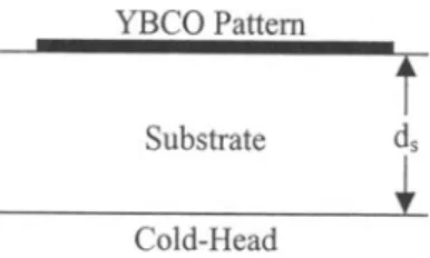
where 1 is the dc bias current, dRidT is the slope of the resistance versus temperature curve at the bias (or operating) temperature, and y]=W/Pt, with W the incident power absorbed by the bolometer, and Pt the total incident radiation power at the surface of the detector. G is the total thermal conductance between the bolometer and its environment, and C is the heat capacity of the bolometer. A sample configuration in contact with the holder is shown in Figure 2.1.
incident radiation
~
supercond uctor
Tx
subsrra leCold- head
Figure 2.1. Typical experimental configuration of a superconductor bolometer on ceramic substrate, with contact to a holder (cold-head).
I
rvI
= 1)1 dRG
-J
1 + (2rcfr)2 dT (2.2)where -c= C/G, and I is the constant dc bias current. Effects due to the variation of the bias current have been studied and can be found in Ref. [7]. If one assumes G and C are constant and independent of modulation frequency, then based on the above model, at frequencies where 2rcft »1, the voltage response ofa bolometer exposed to incident radiation should scale as [-I. The phase ofthe response in any frequency range is:
-2rcfC
e
=
tan-I (-G- )=
tan-I ( -2rcf,) (2 .3)For the studied samples in this chapter, is typically on the order of 0.3 S, hence the 2rch»1 regime holds at as low as a few Hz, where the model above works quite well [7J. However, at frequencies in the range of 100 Hz and above, the measured response of almost all of the investigated samples deviates significantly from the values predicted by the above model [7], [26]. Instead of a [-I dependence, there is a [-112 within the mid frequency range, as shown in Figure 2.2 for a sample with relatively large area pattern with respect to its substrate thickness. The thermal and geometrical parameters of this sample as well as other considered samples in this chapter are given in Table 2.1. To study this frequency behavior, an equivalent circuit model for the bolometric response to radiation signals for modulation frequencies ranging from dc to high values is considered. As shown in the circuit model in Figure 2.3, the response is determined by the total heat capacity of the film as a lumped element, and the film-substrate thermal boundary resistance as well as the thermal constants of the substrate and the interfaces.
.-. >-... I,OOE..o 1 I.OOE·02 :; IOOE..oJ c
..
...
:- IOOE..Q4 '-I'"'
I.OOE'()S lOOE-<J6 I "'<II 01 10 100 1000 10000 Modulation frequency (Hz)Figure 2.2. Measured and calculated IR-response versus modulation frequency of sample 064-04b, at 81.7 K with 0.68 rnA dc bias current and 2.13 mW/cm2 radiation intensity.
Table 2.1. The dimensions of the substrates are about 0.5 cm by 1 cm for all the samples. ds is the
thickness of the substrate, dr is the thickness of the YBCO film, and A is the total area enclosed by the meander line pattern and is roughly twice the area of the meander line. The values of G are obtained at temEeratures above Te.
sample substrate df ds A area of the Tc-onset R(300K) G number material (nm) (cm) (cm2} meander line (K) (k ) (W/K)
064-02a MgO 120-130 0.025 0.075 90Jlmx3.3Scm 87 13.5 33x10-3 064-02b MgO 120-130 0.025 0.0168 SOJlmxl.9cm 86 11.2 IS.SxI0-3 064-03a MgO 170-180 0.05
oms
90Jlmx3.3Scm 82 7.7 Ilx10-3 064-03b MgO 170-180 0.05 0.0168 SOJlmxl.9cm 83 6.5 S.lxI0-3 064-01a SrTi03 220-230 0.05 0.0168 SOJlmxl.9cm 82 10.0 3x10⁻³ 061-02a LaAI03 540-560 0.05 0.075 8SJlmx3.35cm 80 4.4 8x10⁻³ 064-04b LaAI03 190-200 0.05 0.075 90Jlmx3.3Scm 84.5 17.5 7.8xI0-3This section presents measurements and analysis of the magnitude and phase of the response ofYBCO bolometers to radiation signals, with modulation frequencies up to 100 kHz. In this range of frequencies the only film property of importance is dRJdT. Behavior of the IR-response versus frequency to radiation signals in this section is considered to be independent of the radiation wavelength. The effect of Joule heating due to the dc bias current on the response of the samples is also negligible for the test currents used in this section.
A. Calculation of the response
To compare measured results to equation (2.2), one should first determine the dc thermal conductance of the YBCO film to the surrounding environment, G(O), which can be performed in several different ways [2], [7], [24]. The most convenient way is to make use of the slope of the resistance versus temperature curves of the films in the normal state near T c [24]. At high bias currents, the resistance of the bolometer increases due to power dissipation heating the film. This creates a temperature gradient across the substrate and the thermal interfaces. The increase in the resistance of the film due to the Joule heating is [5], [7]:
dR
L'lR=I2R-GdT (2.4)
Using the measured values for R, I, and dRJdT, values of G are obtained and given in Table 2.1.
The heat capacity, C, and the time constant, 't, can be found by use of equation (2.3) as:
't = -(tan8)/2nf = C/G, (2.5)
where 8 is the measured value of the phase of the response. Using equation (2.5) and the
Qt - r T R b d - t i ; l / G b d - t + Ri __ _ RII
+ Cf + Ci
Rs~c= I IGs-c
Figure 2.3. Circuit diagram of thermal model for bolometric response of a high temperature superconductor bolometer.
measured values of8 at low frequencies, 1: is calculated for sample 064-04b and is found to be
-0.32 s at frequencies less than 2 Hz. Using the measured values ofG=7.8 mW/K, c=0.32 s, and dRldT=3850 Q/K (from R versus T curve), the response versus frequency of the sample is calculated for 11=1 using equation (2.2), and is given in Figure 2.2. The calculation is done for 0.68 rnA bias current, 2.13 m W/cm2 incident radiation power with A=0.85 nm and an effective absorbing area of 0.03 cm2, corresponding to the values used in the measurement.
In the calculation of the response, the effect of louIe heating in the film, caused by the bias current, can also be considered. The change in the film resistance due to the input radiation power is augmented by the I2R heating, and is a form of positive feedback. This can enhance the response resulting in an overall responsivity of:
ry_t = (1 - I ry/11) , ry
(2.6) where ry is given as in equation (2.1). As observed in equation (2.6), there is a stability criterion in the voltage response, which has the same form as obtained for dc biasing at zero frequency [1], [7]. Since the bias current in the samples is on the order of 10-3 A, and the
responsivity maximum is on the order of 100 V/W, even at low frequencies, the effect of the louIe heating is negligible as mentioned before. However, in very sensitive devices or at high currents, it could become a significant factor.
The difference between the measured and calculated response at low frequencies is mostly expected to be due to the assumption of11=1. Results similar to those reported by other groups [3], [10] have been obtained for the test samples. As reported earlier and shown in Figure 2.2, the model based on constant C and G, (equation (2.1», can explain the response of the bolometers only for relatively low frequencies, where the response is limited by the thermal boundary resistance, Rs-c, between the substrate and cold head. A more accurate analysis model requires consideration of the thermal diffusion length for the radiation-induced temperature rise into the substrate, and both thermal boundary resistances. At very low frequencies the response does follow equation (2.1) [26], where C and G are constant, and G is interpreted to be mainly due to the substrate-cold head thermal boundary resistance, as verified below.
B. Calculations of the frequency dependent thermal parameters
To study the thermal response of the samples, one can model the substrates as a cylinder and use the heat diffusion equation. In this model the radiation absorbing area is at one end of the cylinder [7], [18]. This assumption will tum out to be valid since the film thickness of samples is much smaller than the substrate thick nesses and the patterns of the superconducting films are relatively large in comparison to the substrate thick nesses (see Table 2.1).
T
Solving the diffusion equation in the substrate material, DV2T
t
,
as a function of the distance from the surface, x, and time, t, and knowing the temperature at the surface will result in [7], [18]:[ .( i21tf 0 )]
T(x,t) = To exp
1 ( D
)5
x-21tft , (2.7)Where To is the temperature at x=O and t=O, D= KsiCs has units of centimeter square per
thermal conductivity and the specific heat (per unit volume) of the substrate material, respectively.
A quantity L, called the "thermal diffusion length", can be used in equation (2.7), and is defined as:
L = (
~f
)1/2. (2.8)It represents the characteristic penetration depth of the temperature variation into the substrate. Considering the thermal diffusion length as the effective length for heat flow into the substrate, the corresponding thermal conductance can be found from [2], [18]:
A
G = aks
L '
(2.9)Where, ks is the thermal conductivity of the substrate material and "a" is a correction factor for the above approximation of the length of the heat flow. Substituting the value of L from
k
equation (2.8) in equation (2.9), and using D = _s_ cs
Gs = a A
-.J
csksnf (2.10)Thus Gs will be a function of frequency and scales as f1l2, increasing with the frequency.
Similarly, the volume of the substrate in which the temperature variation occur changes with the frequency due to the thermal diffusion length. Hence, the total heat capacity, Cs, can be written as:
Cs = b Cs A L = b A-.Jcsks/nf, (2.11)
where b is a constant to compensate for the drop of the amplitude of the temperature variation along L. Hence, Cs will also be a function of frequency and scale as [-112 Under the above assumptions, 1: will be:
Cs b
1: = - = - (2.12)
Gs anf '
which will be frequency dependent, scaling as [-I.
Considering frequencies low enough to allow the total heat conductance Gt Gs and the total heat capacity Ct~Cs, then use of equation (2.12) in equation (2.1), results in;
r'
ry= l+j2b/a ' (2.13)
~ dR .
where r'= Gt dT . Equation (2.13) shows that the phase of the response IS constant and frequency independent for the frequency range where the thermal diffusion length is smaller than the thickness of the substrate. But since Gs scales as
£1.5,
r' will scale as [05, and the magnitude of the response will be frequency dependent. This is valid at frequencies where the thermal conductance of the YBCO film, Gf, and the film-substrate interface, Gtd=l/Rbd, are negligible compared to Gs.The circuit diagram of the proposed thermal model of a superconducting bolometer is shown in Figure 2.3. In this model, the substrate-cold head thermal boundary resistance and the total YBCO film-substrate thermal boundary resistance are considered as Rs-c and Rbd-t, respectively. The substrate is considered to be made of small increments (thin layers of substrate material), which can be shown, by a combination ofRi and Ci in the circuit diagram.
Now, for the overall frequency response analysis (from dc to high frequencies) assume that Cf « Cs and Rbd-t « Rs <<Rs-c (or, Gs-c=lIRs-c « Gs « ~d-t=lIRbd-t), which will be shown to be the case for the samples in table 2.1. Where Rbd-t is the total thermal boundary resistance at the film-substrate interface. Based on these assumptions, at very low frequencies, the heat capacity of the film can be ignored compared to that of the substrate, and the total thermal conductance will be:
1 1 1 1
- = -+ - + - - (2.14)
Gt Gs-c Gs ~d-t
Since Gs-c « Gs(O) « ~d-(, we will have Gt ~ Gs-c which is not frequency dependent. Then, the response can be obtained from [7]:
1
t1Tf= Gs_c+j2rrfCsCO) W, (2.15)
Where t1Tf is the temperature variation at the film and 'to =Cs(O)/Gs-c. Then, ignoring the effect of the louie heating, the responsivity of the bolometer is given by equation (2.1) with a frequency dependence of f1, and a phase angle of -90 degree, for frequencies at which 2rrf» 1, but not so high as to limit the thermal diffusion length.
When the frequency increases to the values where the thermal diffusion length in the substrate, L, becomes comparable to the thickness of the substrate, G and C will no longer be constant. Based on the above assumptions, G "" Gs and C ~ Cs, they are frequency dependent following equations (2.10) and (2.11) respectively, and the response is governed by:
_ 1)1 dR
rv - Gs+j2rrfCs dT ' (2.16)
Where still Cf « Cs, Gs « ~d+ By applying the frequency dependence of the Gs and Cs in equation (2.16), the response will be in the form of equation (2.13), i.e. rv_fll2 As the frequency increases further, Gs(f) increases further (or, Rs(f) decreases) until it becomes comparable to ~d-t where Cf and Rbd-t can no longer be ignored. At high enough frequencies, the Gs and Cs can be ignored and the response will be determined by ~d (or 1lRbd) and Cf [7], [15], [17].
C. Frequency response analysis and the experimental results
Based on above analysis, the point at which the response start to scale as fll2 occurs at frequencies where the thermal diffusion length, L, becomes comparable to the thickness of the substrate. Since from equation (2.8), L is proportional to the square root of the thermal diffusion constant, D=ks/cs, substrate materials with higher ks, will have knee points in the
Table 2.2. Thermal characteristics of single crystal substrates Substrate ks(WIK-cm) cs(JlK-cm3) D(cm2/s) fL=O.OScm(Hz)
MgO 3a O.53a 5.66 720 LaAI03 SrTi03 "Prom Ref. [2] 0.32b 0.052c b 0.59 0.43c Prom Ref.[17] 0.55 0.12 'Prom Ref. [6] 70 15.4
UlOE-02
...
I.OOE-Ol > ~..
..
c: g, l00E-OC"
..
..
,
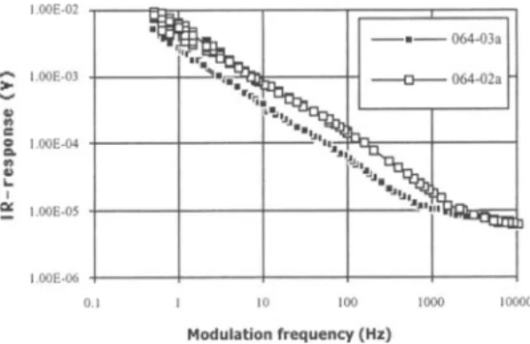
a: LOOE-OS 100E-06 01 10 100 1000 10000 Modulation frequency (Hz)Figure 2.4. Measured IR-response versus frequency for 0.05 cm thick MgO substrate sample 064-03a and 0.025 cm thick MgO substrate sample 064-02a.
response at higher frequencies (assuming the substrate thick nesses are the same and Cs of the substrates are within the same range). The values ofks, Cs and the calculated frequency of the knee point, fL, of three different substrates used in this chapter are given in Table 2.2 The value of Cs for LaAI03 in Table 2.2 is derived using the phase of the low frequency response [7]-[26], and is consistent with the measured experimental values shown for MgO and SrTi03. The values of fL are calculated by use of equation (2.8). For example, to find the frequency at which the thermal diffusion length is 0.05 cm for a SrTi03 substrate, one can use equation (2.8) in the form of:
D
fL =
nO
(2.17)For the SrTi03 substrate from Table 2.2: ks 0.052
D
=Cs'
= 0.43=
0.121 cm2/s (2.18) Applying equation (2.18) and L=0.05 cm in equation (2.17), results in fL = 15.4 Hz as given in Table 2.2. The measured responses versus frequency for 0.05 cm thick single crystal LaAI03, MgO, and SrTi03 substrates are shown in Figures 2.2, 2.4, and 2.5 respectively. From the figures, the knee points in the response versus frequency are about 15 Hz, 60 Hz, and 600 Hz, for 0.05 cm thick SrTi03, LaAI03, and MgO substrates, respectively, in good agreement with the calculated values in the table.To verify the above analysis and to investigate the effect of the thickness of the substrate on the frequency response, we consider two samples with identical meander line patterns on 0.25 mm and 0.5 mm thick MgO substrates. The response of the samples 02a and 064-03a, are shown in Figure 2.4. As shown in the figure, the knee point is found to be dependent on the substrate thickness, and it is found not to be dependent on the pattern area. The knee point for the thinner substrate sample 64-02a occurs at higher frequencies, about 2.5 kHz to 3 kHz, whereas for the thicker substrate sample 64-03a, it occurs at about 700 Hz to 800 Hz. Setting the thickness of the substrate equal to L in equation (2.17), and using the values of Cs and ks from Table 2.2 for MgO, knee points at frequencies of 720 Hz and 2.8 kHz are calculated for samples 64-03a (0.05 cm thick) and 64-02a (0.025 cm thick), respectively. The above calculated values of frequency agree with the break frequencies seen in Figure 2.4.
I.OOE-<)2 _ IOOE-03 >-~
.,
"
c..
100[·/)4...
"
.,
..
I'"
1 00[.0) 1.00E-06.r
I-"it>,><,~,.,
!
! !
I
~!!I.~I"I ",n,,, .. ,,, ,,,,,,,,,,,,,,,,, """·'tl..···"1
100£·01 1.<10[<00 I.OOE~I I.OOE+02 I.00E~l 1.00£.'" 1 OOE~'
Modulation frequency (Hz)
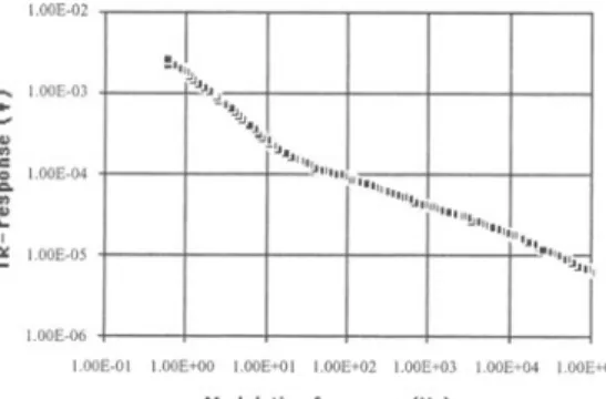
Figure 2.5. IR-response versus modulation frequency of SrTi03 substrate sample
064-01a measured at 0.25 rnA bias currents.
From equation (2.13), for frequencies higher than fL, the phase should be frequency independent. Figure 2.6 (next page) shows the measured phase of the response for sample 064-0 I a, which confirms the position of the break frequency discussed above. The flat region in Figure 2.6 extends only to about 10kHz, but it should continue up to the frequencies where the response and its phase starts to be governed by the effect of Rbd, according to our model. Since the YBCO film is just a few 100 nm thick, the heat capacity of the film, Cf, is very low, and the phase of the response should approach 0° for the frequency range where the response is limited by the effect of Rbd, and continue until much higher frequencies. The frequency at which Rbd, the film-substrate thermal boundary resistance, becomes important varies with the thermal parameters of the substrate material. It is lower for substrate materials with higher ks (assuming Cs of the substrates are within the same range) [7]. Using Cs and ks from Table 2.2, and a typical value for Rbd as l.JxlO-3 K-cm2/W [17] , one can compare this with the frequency dependent thermal resistance of the substrate, as calculated from equation (2.10). The thermal resistance due to Rbd is equal to the thermal resistance of MgO, LaAl03, and SrTi03 substrates at modulation frequencies of 165.4 kHz, 1.413 MHz, and 11.67 MHz, respectively. These frequencies are calculated for the case that the corresponding thermal diffusion lengths are small compared to the width of the meander lines of the superconducting pattern, which is the case in the samples of Table 2.1. For smaller patterns, the spacing between the lines should also be considered. This will result in frequencies lower than above [7].
One can estimate the frequencies at which Rbd and Cs would change the phase, and this is 10 to 50 MHz range. Hence this cannot account for the drop in the phase seen in Figure 2.5. The drop in the phase at frequencies of about 10 kHz is also observed for samples with MgO and LaAI03 substrates. This departure from our model for the thermal response of the samples may be due to other effects, such as the system circuitry [7], or photo-induced conductivity changes in the YBCO film [34]. However, this analysis accurately accounts for the observed behavior below 10kHz. To summarizes this section, the slope of the response changes at "knee" frequencies of about IS Hz, 60 Hz, and 600 Hz for 0.05 cm thick SrTi03 , LaAI03, and MgO substrates, respectively, from a [I to a [05 dependence. From equation (2.1), one sees that a high G value, G»2nfc, lowers the responsivity, and pins the phase of the response at
-1 0 + -1 - - f - - + - - + - - - - 1 - - - I - - - l .20 +1
- --if--+---+----+--+----I
.l0 t---~---1I----1 ~I
11 , 'I." n llll l'lilll"I~1 1 _1_ .. . ~ -40 +----~ fill'''·' I I !Ill. ~~ f ~"1 "'iiI.,_&) .So ~~.,. ".ij • •
.: -60
~.!o.
;"
;~~
Q.
1 ..
""j--,~II:!
.70 ~1.liil"j
7
::
.j.1----l---~--+---+---l---~
looE·OI l.ooE<OO l.ooE'OI I.OOE+02 I.00E;{)l l.ooE~ I.00E+Ol
Modulation frequency (Hz)
Figure 2.6. Phase ofIR~response versus modulation frequency of sample 064~01a
(0.05 cm thick SrTi03 substrate).
8=0°. A low G value, G«2n:fc, gives 8 = ~ 90°, a [-1 dependence to the responsivity, and a magnitude inversely proportional to the heat capacitance of the bolometer. For this latter case a very thin substrate to reduce C is indicated. While G can be made very small by isolating the substrate (underneath the pattern) from the cold head, the minimum G(O) is needed to keep the sample in the superconducting state, and within a DoT of its bias temperature. For the considered samples here with G's on the order of 1O~2 W/K, Joule heating power on the order ofI2R=10·2 W yields a shift temperature on the order of 1 K. Hence as a practical matter, a G much smaller than the values in table 2.1 would present a problem in maintaining the bias temperature for currents on the order of 1 rnA.
3. ANALYTIC THERMAL MODELING FOR DC TO MIDRANGE MODULATION FREQUENCY RESPONSE
There has been different efforts on the response modeling of the edge~transition
superconducting bolometers with and without the consideration of the effects of the thermal boundary resistance at the substrate interfaces and the self or Joule heating in the superconducting film [16], [35], [30]~[31]. Based on the above proposed effects of the introduced parameters, section 2 discussed successful analysis and prediction of the behavior of the response versus modulation frequency curves predicting the frequencies at which the slope of the curve changes (the knee frequency) [7], [16]. Though, one cannot predict and match the response in all the measured modulation frequency regimes using an analytic model. Using the analyses in section 2,one can predict and match the measured response of the samples at very low frequencies showing different considerable discrepancies at midrange and/or higher modulation frequencies [7], [16]. In many of the proposed models and the solutions, only the magnitude of the response have been considered and compared to the experimental values. This is while the phase of the response is a more sensitive characteristic of the response with respect to the model and the chosen or obtained thermal parameters of the devices [24]. In this section the results obtained from a recent closed form solution of a comprehensive one-dimensional thermal model is discussed. The results from the model are compared to the both measured values of the magnitude and phase of the response of the samples.
Va ~fs ••• ~+ . . . Rs + Cs Rsc ,m·l Sub,lmle x9l
Figure 3.1. Equivalent thennophysical diagram of the bolometers in contact with the holder, Where q is input radiation power, Cr is lumped heat capacitance of the film, Rfs and
Rsc are the thennal boundary resistance values at the substrate interfaces.
A. The Thermal Modeling
From the given dimensions in Table 2.1, the area of the superconducting pattern of the samples is large with respect to the substrate thickness. Hence a one-dimensional model is considered and applied for the studied samples while considering all the parameters for per w1it area. Because of the partial lateral heat diffusion of the coming heat wave from the film into the substrate (the spreading resistance effect), a correction factor, a, is considered for applying to the measured Rse values and is obtained and given for some of the samples in Table 3.1. The value of a increases with the increase of the thermal conductivity of the substrate material and being the highest for MgO. It increases with decrease of the superconducting pattern area with respect to the substrate thickness as given in the table to be higher for the small pattern film on SrTi03 compared to that of the LaAI03 substrate sample. As given in the tables, the thickness of the superconducting films of the samples is also very small compared to that of the substrate. This allows the consideration of a lumped film assumption on top surface of the substrate in the model.
Considering the superconducting pattern as a lumped film and substrate as a continues uniform media, the thermal equivalent circuit of the samples in contact with the holder can be represented as in Figure 3.1, where q is the absorbed radiation intensity at the surface of the sample. In this equivalent diagram, two thermal boundary resistances are considered at the substrate interfaces. The heat capacitance of the superconducting film is also considered to be a value representing the total heat capacity of the film per unit area. The thermal conductance of the superconducting film is calculated to be negligible compared to that ofthe substrate and the interfaces. For samples with thicker superconducting films as for the screen-printed materials [4], the limited heat conductivity of the superconducting material same as for the substrate, should also be considered. Based on the above considerations in the model as
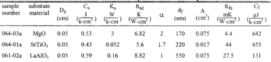
Table 3.1. Dimensions and the obtained thennal Earameters of the samEles used in the model.
sample substrate Cs Ks Rsc
df Rfs Cf
number material Ds
J W K a A mK
(em2) ~
(em) (k_emJ ) (k-em) (W-em2 ) (nm) (W-cm2 ) (k-em-)
064-03a MgO 0.05 0.53 3 6.82 2 170 0.075 4.4 642
064-01a SrTi03 0.05 0.43 0.052 5.6 1.7 220 0.017 44 655
shown in Figure 3.1, the derivation of the temperature variation and the corresponding thermal parameters for the samples under a constant bias current is presented in the following.
a) Temperature Variation in the Substrate
To approach the complete closed form solution to the model given in Figure 3.1, first one can consider the absorbed radiation power, q, is applied directly to the surface ofthe substrate. This is ignoring the effects of the surface boundary conditions of Cf and Rfs, which are representing the effect of the thermal parameters of the superconducting film at this stage. This particular assumption and the solution to it would be the case as for very low modulation frequencies. At low modulation frequencies, Cf is much smaller than the contributing heat capacity of the substrate, which can be determined from equation (2.17) [7]. Also the film-substrate thermal boundary resistance, Rfs, is much smaller than that of the film-substrate-holder and/or the low frequency thermal resistance of the substrate, Rs=lIGs, determined from equation (2.10).
Based on the above assumptions and the steady state solution to general one dimension heat propagation equation, the temperature variation at the surface of the substrate, t.T, can be obtained. Without the consideration of the effect of the superconducting film (i.e. Cf and Rfs)
t. T follows;
t.T= eXP(YL)+reXP(-YL)V 1 3 1
q exp(yL)-rexp( -yL) jUlcsks ( . )
where y is the characteristic thermal impedance of the substrate material defined as;
I+j~ ~
y7z\jk;
(3.2) And; Rsc -(3.3) r=~'
Rsc+ -. -k-JUlCs sWhere Ul is the angular modulation frequency, and ks and Cs are the heat conductivity and the heat capacity of the substrate materials, respectively. The value ofRsc can be obtained;
R= 1 (34)
sc G(W/K)/A' .
Where G is in units of W /K and is the total thermal conductance of the device at very low frequencies, G(O), and A is the film pattern area. This is based on the assumption of Gfs » Gs »
Gsc where Gfs=lIRfs, Gs is the total heat conductance of the substrate, and Gsc=llRsc. This assumption is verified for the samples with dimensions close to that of table 2.1 and 3.1, which is also discussed in section 2 [7], [16], [22]-[24], [37].
b) Temperature Variation at the Film
To find the voltage response to the modulated radiation intensities, the temperature variation in the superconductive film of the samples can be obtained for all considered frequency ranges. This temperature variation corresponds to the temperature change across Cf in the equivalent circuit of Figure 3.1. Hence the only temperature gradient from top of the superconducting film into the substrate would be that across the film-substrate interface, Rfs.
Solving the one-dimensional thermal differential equation with the complete boundary conditions as shown in Figure 3.1 (i.e. with the consideration of Cf and Rfs), the temperature variation caused by the radiation absorption in the film follows;
( exp(yL)+f'exp(-yL) _1_+ R
l
eXp(YL)~f'~X~(-YL)
'co jcocsks . fs~
~r"~L
1 ' . - . , r " J L"exp(yL)-f'exp(-yL)
\J
VS'~S /(3.5)
Where, q is the absorbed radiation power in the film per unit area, and Cr and Rfs are the total heat capacity of the superconducting film and the thermal boundary resistance at the film-substrate interface per unit area, respectively.
The solution of equation (3.5) is up to frequencies where the thermal diffusion length into the superconducting film (for YBCO material) becomes smaller and/or comparable to the thickness of the film. This is while the penetration depth and/or the absorption coefficient length in the superconducting film is still considered to be much smaller than the film thickness. This frequency regime for the samples of II_Table 3.1 with a maximum film thickness of about 550 nm much higher than that considered here. As given in equation (3.5), at very low frequencies the denominator will approach one and the Rfs will become negligible compared to the first term of the numerator leading to the results of the one boundary condition problem as given in equation (3.1). This is because at very low modulation frequencies the temperature variation (heat wave) reaches the bottom of the substrate and hence the heat capacity of the film with respect to that of the whole substrate material under the pattern, and also the thermal boundary resistance at the film-substrate with respect to Rs and Rsc become negligible [7], [37].
c) The Voltage Response and Bias Current Dependence
Considering a uniform temperature variation in the film, caused by the absorbed radiation, L1T, the voltage response in a dc current bias configuration can be obtained from;
dR
L1V=IbL1TdT' (3.6)
Where Ib is the dc bias current, dRidT is the slope of the R versus T curve at the bias temperature as given in II_Table 3.1, and L1T is the temperature variation in the superconducting film as given in equation (3.5). Equation (3.6) is valid within the temperature variation range where dRidT can be considered to be constant. The maximum temperature variations of the films caused by the radiation is typically below about a few mK. The transition widths of the samples are typically of a few degrees of Kelvin and hence the variation of dRidT and/or the non-linearity of equation (3.6) are negligible in the measured and calculated response. Though this would not be the case for devices exposed to high radiation intensities, which are normally voltage biased for further stability'S [12]-[13]. The effect of the bias configuration on the response and the feedback effect of the Joule heating for each case of the voltage-biased and current-biased configurations are discussed elsewhere [25].
There is also a consecutive temperature variation due to ac Joule heating in the film caused by the resistance variation in the superconducting film due to the input radiation power. This effect on the response is in the form of a positive feedback in the used current-biased configuration. This ac Joule heating in a first order approximation can be considered either as a dependent radiation (or heating) source in parallel to the external radiation source,
q, shown Figure 3.1 [40], or simply as an additional term in the overall responsivity of the sample discussed in section 2. The effect of ac Joule heating in the response of the samples studied in this work is negligible for the used biased currents.
B. Measured Frequency Response and the Results From the Model
The results from the model were compared to the experimental values for the samples given in II_Table I. The frequency response behavior of the samples was found to be strongly dependent on the film and substrate dimensions as well as on the thermal parameters, while the observed dependencies are in good agreement with the thermal model. To calculate the response using equation (3.5), the dc thermal parameters of Rfs, Rsc, Cr, Cs, and Ks of the samples were determined. The measured values of the above parameters are given in II_Table 1. The values of Rsc, which are much higher than Rs and Rfs, are measured using the method of the resistive or the dc Joule heating in the film close to the transition temperature, Tc [5], [24], [39]. In this method a high bias current is passed through the film and the temperature rise due to the Joule heating is measured by measuring the resistance of the film. Then knowing the temperature rise and the Joule heating power the values ofRsc are obtained. Also the parameters such as the film-substrate thermal boundary resistance and the thermal parameters of the substrate or the heat capacity of the samples could be obtained and verified using the fit of the results from the model to the measured values. The above values in II_Table 1 are given per unit area as used in the one-dimensional solution of the model.
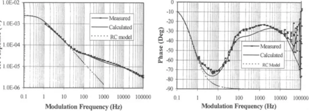
The results from the model were investigated for thin film samples on crystalline SrTi03, LaAI03, and MgO substrate materials. The measured and calculated magnitude and phase of the response of the meander line patterned YBCO films on the 0.05 thick SrTi03, LaAI03, and MgO substrate samples are shown in figures 3.2, 3.3, and 3.4 respectively. Calculated response using the basic R-C model in section 2 (equation (2.1)) is also plotted for samples 064-01 a and 061-02Aa.
As discussed in section 2, the basic R-C model is as useful as the complete model in the very low frequency ranges where the thermal diffusion length into the substrate is much larger than the substrate thickness. This basic R-C model is appropriate for micro machined and/or freestanding film bolometers. The G and C values of such bolometers would be constant up to
10E-02 ! I .11 'I I •. , ,. ,. ,11111 11,11 ~ 100-OJ ~ c 8. I 0E-04 ~
:!:
1.0E.05 I OE.Q6 , '1 1'1" 1 '11'1 01 I 10 100 1000 10000 100000 Moduliltion frequency (Hz) 0 ·10 ·20i
630e
-40 ~ ·50'"
f -60
·70 -80 ·90 0 1 10 100 1000 10000 100000 Modulation frequency (Hz)Figure 3.2. Measured and calculated magnitude (left) and phase (right) of response versus modulation frequency of the SrTi03 substrate sample 064-01a at 80 K and 250 rnA dc bias current.
,,11111 0
\ OE-02 [ I! \\ui 'lull 11.11'1. II ' .,' II Iii
-10 ", -20 >" 1.0E-03 b1 -JO ~
...
~6 40
c: ~ 1.0E-04 ~ -50.,
f ~ '-~ IOE-05 -70 -80I OE-06' i' 111'1 ,Iilll!, , ';"\ IIIII ~ 1111111 , , , 1111,11 -90
I II I I II 'I 1 illl' I. ,
N
I
----
'III -1,11"b-tI 11, ~I .l
I , ' ~ IY~~
I
,1 -M=IRd ''\II
illl - CalcuialCd f,--i I I~ , I) I 'I --- -RCModdf--'n
I " , " . ,Ill
,
''"!J; ..;.L
1111 ~_,. 'III I', I'll'
O. I 10 100 1000 10000 100000 0.1 I 10 100 1000 10000 100000
Modulatioll Frequency (Hz) Modulation Frequency (Hz)
Figure 3.3. Measured and calculated magnitude (left) and phase (right) ofresponse versus modulation frequency of the LaAI03 substrate sample 061.02a at 80 K and 500 JlA bias current. The
response is calculated from both the analytic model and that from the basic RC-model. very high frequencies where the thermal diffusion length into the substrate or into the micromachined free standing base element of the bolometer becomes smaller or comparable to the thickness of the substrate or the base element [38]-[39]. In general the use of the basic R-C model is appropriate in the frequency regimes where one period of the modulation frequency is longer than the low frequency time response of the samples, 'tL. The 'tL is defined as 't L=C(O)/G(O), where G(O) and C(O) are the total low or so called the dc thermal conductance and the heat capacity of the samples_ In the following the results from the model to the measured values are compared and the effects of different thermal and dimensional parameters on the fit of the model to the experimental values are investigated. The comparison is done for both the magnitude and phase of the response in three regimes of low, mid, and high ranges of frequencies .
a) The Magnitude of Response at Low Frequencies and the Dependence on the Substrate Material and Dimensions
As given in Table 3.1, the substrate-holder thermal boundary resistance of the samples, Rsc, are given in per unit area and found using the measured dc thermal conductance of the samples using the shift in the temperature caused by Joule heating at elevated bias currents
10&02 i 0 -10
f
IOE-(lJ -20i
·30 e::"
e.
-40 g, 10&04 ~ ·50 !J..
t, -60 ci: 1.0E-05 -70 -!OI 0E-06 , ., ""1 I I :1~ , , , 11 i li"'1 lilli"
-90
01 10 100 1000 10000 100000 01 10 100 1000 10000 100000 Modulation Frequency (Hz) Modulation Frequency (Hz) Figure 3.4. Measured and calculated magnitude (left) and phase (right) ofresponse versus frequency of the MgO substrate sample number 064-03a at 79 K and 1 rnA bias current. The
[24]. As introduced before the factor a is defined for the correction ofRsc value and depends on the area of the pattern, A, the substrate thickness, d" and the thermal conductivity of the substrate materials, k,. It increases by the increase of k, and the increase of the ratio of dsl A as expected. The requirement of the factor a for a better fit of the calculated response curves to the measured ones, is due to the spreading thermal resistance effect in the substrate material neglected by the one dimensionality of the model discussed here. Hence, for a relatively low thermal conductive substrate sample with a small dsl A ratio, this factor is expected to approach one as observed in table 3.1. Using the known parameters for the films and the substrates and the obtained values for the a and the boundary resistance', the phase and magnitude of the response for the samples are calculated and plotted in figures 3.2 to 3.4.
As shown in the figures, at low modulation frequencies there is a discrepancy between the results from the model and the measured values. This discrepancy increases by the increase of the thermal conductivity of the substrate materials showing its maximum for the most conductive substrate material. This is due to the one dimensionality of the model ignoring the lateral heat diffusion in the substrate materials underneath the pattern. By comparing the magnitude of the response curves in Figures 3.2, 3.3 and 3.4 for SrTi03, LaAI03, and MgO respectively, the discrepancy is the most for the most thermal conductive MgO substrate sample. This is also consistent with the variation of a, which is the highest for the same sample. This discrepancy can be avoided by use of a three dimensional solution for the model, or use of an approximate cylindrical solution for a truncated cone structure with a linearly increasing base from the film to the bottom of the substrate. Such approximate solutions can also be applied using the simulation programs such as SPICE where the parameters can further be considered frequency dependent [7].
b) Phase of the Response and the High and low End Frequency Behavior
The phase of the response of the samples are much more sensitive to the values of the characteristic parameters of the samples. Particularly the drop of the phase at high-end frequency response has been the determining factor in finding the equivalent values of Cf and Rfs given in Table 3.1. While the low end calculated phase of the response is in a very good agreement with the experimental results for SrTi03 and LaAl03 substrate samples, there is a peak at the frequency range of 10 to 100Hz in the MgO substrate sample, which cannot be explained by this model. This behavior has also been observed for all other MgO substrate samples. This occurs at lower frequencies in thinner substrate samples e.g. at about 10 to 20 Hz frequency for 0.025 cm thick MgO substrate samples compared to that of a 0.5 cm thick MgO substrate sample 064-03a shown in Figure 3.4b. One speculated mechanism for this is possibly due to the reflection and interference effect of the acoustical phonons within the boundaries of the substrate underneath the superconducting pattern [24]. The possible effect of the superconducting material on the spectral phonon density in the substrate and its consequent effects is discussed in next sections.
c) Mid-Range Frequency Behavior of the Phase and Magnitude of the Response
There is a slight discrepancy in the midrange frequency response curves compared to that of the model. This is clearly seen in the plateau of the phase versus frequency curves for all the samples shown in Figures3.2 to 3.4. The discrepancy is also seen partly in the magnitude of the response curves in the same frequency regime. The measured response in this range is slightly higher in magnitude, and more in phase with the radiation signal than the expected values from the model.
7
b..!
"-~-l:!--l---j---r""""J
t m
i
"'< \,
....
;
/±\"
"~/
<,
:
:3 "''' : .... • c:~
"" • -' , 1---1---;\ I"· I Time (IOmSec.lDiv.)Figure 3.5. The steady state response versus time of the SrTi03 substrate sample
064-01 a at 560 IlA bias current, radiated by a 20 Hz square radiation signal with
2.13 mW/cm2 maximum intensity.
The possible effect of the radiation absorption by the open areas of the substrate within the meander lines of the patterns has also been investigated as a possible source for the discrepancy. This consideration in the model Leeds to lower phase of the response increasing the observed discrepancy in the plateau region of the phase curves particularly for the SrTi03 substrate sample. The spectral absorption of the crystalline substrate materials from 600 run to 50 !lm are about 12%, 20%, and 8% for the 0.05 cm thick SrTi03, LaAI03, and MgO substrates at 850 run radiation wavelength respectively. While the effect of the substrate absorption is negligible in the response of the samples measured at 850 nm radiation wavelength, it has a major effect in the measured spectral response of the samples at longer wavelengths [7], [9], [11], [37]. The effect of the substrate absorption in the spectral response of the samples is studied in next sections.
A small and relatively fast component in the time response of the samples also is reported which relatively increases compared to the total response as the modulation frequency increases. This cannot be explained by the thermal response as modeled in this work. The steady state time response of SrTi03 substrate sample 064-01 a in the above mentioned frequency regime, is shown in Figure3.5. As observed from the figure there exist an abrupt jump and drop at the edge of the on and off switching times of the radiation source. The source is a fast near IR source, which is derived by a square wave voltage signal. The same type of the steady state time response is observed for all other samples in the same frequency regime. The effect of this fast component of the response is in the favor of the discrepancy (i.e. lowering the phase value and increasing the magnitude of the response from those calculated values by the model). This is possibly the non-thermal component of the response and being a possible source for the discrepancy that needs to be further investigated.
C. Response of thick film ETBs
Thick film IR detectors are typically fabricated by screen-printing technology using pastes manufactured from high-Te superconducting powders on polycrystalline substrates such as MgO and Ab03 [4]. The thickness of the superconducting films obtained by this method is in the range of a few lOs of micrometers, being about 30 !lm for the studied samples here. The Y-Ba-Cu-O compound with 123 and 124 stoichiometries can be used for fabrication of thick film superconductive infrared detectors using the hybrid technology. The fabricated films are then post annealed in various ambient such as Oxygen at high temperatures resulting granular
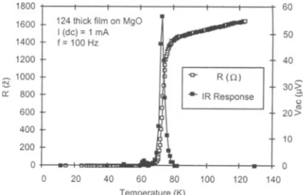
1800 1600 1400 1200 _ 1000 t!-o: 800 600 400 200 a a
124 !hick film on MgO I (de) = 1 mA f = 100 Hz 20 40 60 80 Temperalure (K) 60 50 40 -<>- R(O) ... IR Response 30~
"
20> 10a
100 120 140Figure 3.6. Resistance and magnitude of the response versus temperature of a 100 /-lm wide and 4mmx6mm total area thick film YBCO on MgO substrate sample.
superconductive films with a 123 phase [29]. The thick film samples here are screen printed on polycrystaUine MgO substrates. The film geometry are a serpentine pattern, with a line of 250 /-lm width and 82.6 mm length, 0.89 mm pitch and 30-35 /-lm in thickness [4].
At sufficiently high annealing temperatures, about 850°C in air, the detectors made of material with 124 phase of YBCO converts to the 123 phase plus a CuO species. The conversion of 124 material to 123 + CuO at high temperatures can give 123 material with higher critical currents [29], permitting a higher bias current for the bolometer. The CuO species, considered to be uniformly distributed in the bulk, can behave as pinning centers for fluxons and prevent flux flow in the material [24].
The IR-response versus temperature measurement on a 124-based sample (converted to 123 phase) is shown in Figure 3.6. The results of the IR-response vs. temperature measurement are superimposed on its R vs. T transition curve in the figure. It should be noted that there is a small peak at 60 K to 65 K in the response, which is below the region of its transition-temperature curve (T<Tc-zero), A similar feature is not reported in the IR-response of
the sample at lower dc-bias current. This response, which shows a dependence on the dc-bias current through the sample, is attributed to a Kosterlitz-Thouless phase transition and the associated noise signal below ~Tc as discussed in section 7,
10 ;; .a
.,
~
<Il &! '"..
~ 1 '\ \ 10 124 film on MgO ==rT = 76,5 K -I (de) =100 ~A "\, IR power =1 ,43 mWlcm 2"-r'.
' -
I~
I 100 1000 10000 Frequency (Hz)Figure 3.7. Magnitude of the response versus frequency of a 100 /-lm wide and 4mmx6mm total area thick film YBCO on polycrystalline MgO substrate sample,
An IR-response vs. frequency measurement on a thick film is shown in Figure 3.7. As shown in the figure, there are two breakpoints in the response. The first breakpoint, near 400 Hz, is attributed to the thermal time response, T (CIK), of the substrate and matches the preceding analysis with respect to the effect of the substrate-holder thermal boundary resistance. The second breakpoint, near 800 Hz, is attributed to the thermal time response of the thick superconducting film with the consideration of the film-substrate boundary resistance. Considering this assumption, the second breakpoint is expected at much higher chopping frequency for thinner films as discussed earlier.
4. THE TEMPERATURE DEPENDENCE OF RESPONSIVITY AND DEVIATIONS FROM THE DRIDT CURVE
The phase and amplitude of the response to infrared signals of edge transition bolometers versus temperature is studied in this section. The measured amplitude and the phase of the response versus temperature of the devices deviate from that expected based on the discussed models in the preceding sections. In this regard a model is discussed here that can explain the observed discrepancy in the response versus temperature from the dRldT curve in the studies samples in this chapter and some of other reported discrepancies from the bolometric response in the literature [22]-[23], [45]. Based on this model, the thermal constants, G, and C, change as the film goes into the superconducting state; G becomes strongly temperature dependent, and decreases with decreasing temperature. A probable cause for the change in G is a shift in the nature of the phonons emitted by the superconductor as it goes through Te.
There is a dependence of the measured total dc thermal conductance, G(O), on the thickness of the substrate of the samples. Based on the preceding analysis, G(O) is always limited by the substrate/cold-head thermal boundary resistance at low modulation frequencies [7], [18]. This conclusion is confirmed by comparing the results to a model of the device's frequency response as discussed earlier. Also using the low frequency response of the bolometers, the specific heat and thermal conductance of the substrate material can be verified to confirm the a above approach [7], [18]. The study of this part has been focused on the characteristics of YBCO films on MgO substrates samples in response to infrared radiation with a wavelength of A=0.85 nm emitted from a near IR-LED source.
A. Thermal conductance characterization
As discussed earlier, the thermal conductance of a bolometer is defined as the total heat conduction from the bolometer to its environment per degree of temperature difference. The amount of input power (heat), Pin, to a bolometer can be determined, and used to measure G from:
Pin
G= l'.T ' (4.1)
where l'.T is the difference between the temperature of the bolometer and its environment. The thermal conductance of a superconductor bolometer can be measured in different ways, which are discussed here in more details. In each technique there are different kinds of possible error associated with the nature of the characterization [7], [24]. Heat loss by radiation from the superconducting bolometer (superconducting film and the substrate) in typical systems is nonnally negligible compared to the phonon heat conduction [7], [30].
One of the effects of the finite thennal conductance in a sample can be observed in the R versus T curves at different bias currents. The thennal conductance of the sample puts a limit on the maximum bias current that can be used in the measurement. The bias current at any temperature higher than T c-zero, is limited by thennal runaway, characterized by the factor a
defined as [I]:
r
2dR . . . . b'I' (4 2)a = G(O)dT; with a< 1 reqUired lor sta I lty, .
where I is dc bias current and G(O) is the dc thennal conductance. The effect of instability in the temperature of the film, due to high bias currents, will appear as an umealistically sharp transition in the R versus T curve [25], [42]. The instability and the shift in the T c-onset can be used to measure G(O).
At low bias currents the temperature of the superconducting film is very close to the temperature of the cold-head. As the bias current increases, a temperature gradient develops across the substrate and the interfaces due to Joule heating in the film. Since it is the temperature of the holder which is commonly controlled, this results in a shift of the bias point in the superconducting film towards Tc-onset where dRJdT has lower values. The decrease of
dRJdT lowers the detector response [25], which has been interpreted as the effect of the bias current on the intrinsic part of the response by some groups [22]. The drop of the response at high currents can be used as a different method to measure G. Knowing the dRJdT versus T curve, and the change in the response, the shift in the temperature of the superconducting film with respect to the holder can be found. Using the R and the bias current, the power dissipation in the film can be obtained. Then by use of the temperature shift and the dissipated Joule power in equation (4.1), the value ofG(O) can be calculated [24].
The most convenient way to obtain G(O) is to make use of the slope of the R versus T of the films in the nonnal state near Tc as shown for sample 064-02b in Figure 4.1. At high currents, R increases due to the dc power dissipation heating the film. The relationship between the increase in the resistance of the film, R, and the bias current due to Joule heating is:
dR
~R= 12RGdT (4.3)
Using the measured values for the dRJdT at the bias temperature of the holder, and the bias currents, values of G can be obtained for each data point. There is a slight error in the above
6 r---~ 10 i :::>
~ 3
a! a I ...-= 60 70 eo Temperature (K) 90 100Figure 4.1. R versus temperature of sample 064-02b at 100 IlA bias curren! and 2 Klmin heating rate. Insert shows full temperature range.
method due to the change of the dR/dT at different temperatures.
Here one can use a method, which eliminates the above error. Considering louIe heating by the bias currents as the source for the shift of the film temperature, T f, with respect to the temperature of the holder, G(O) can be found from:
J2R
G(O)= t.T (4.4)
where t. T is the difference between T f and the temperature of the cold-head. The resistance of the film, R, can be measured from
v/r
at each point. Using the R versus T curve for the region of interest (90<T<120K), and the measured value of R at different bias currents Tf can be obtained and used to determine t.T. Then using t.T and Pin= r2R in equation (4.4), values of G(O) can be obtained for each data point. This is the method used to find the averaged values given in III_Table 2.1. To measure G(O) relatively high bias currents should be used for ease in monitoring the temperature change in the film. However, high currents through the material can affect the electrical properties of the films shifting Tc to lower temperatures [25], [48]. B. Dependence of G on the YBCO film pattern and the substrate thicknessThe values obtained for the dc or low frequency thermal conductance of the studied bolometers are about 2-3 orders of magnitudes lower than the values calculated from the properties of the substrate material, which can be obtained from:
A
G=ky. (4.5)
Where k is the thermal conductivity of the substrate material and L and A are thickness of the substrate and area of the superconducting pattern. The substrate/cold-head thermal boundary resistance determines the measured G values in III_Table 2.1 [7], [25]. This can be found from the frequency response of the devices. At low frequencies, the thermal diffusion length into the substrate, Lf [2], [7], [18], [60], is larger than the substrate thickness, and G is constant with respect to f, and much lower than the values calculated for the substrate from equation (4.5). As the frequency increases, Lf becomes comparable or smaller than the substrate thickness changing G, which changes the slope of the response versus modulation frequency from a [1 to a [05 dependence [2], [7], [16]. Then G is limited by the thermal conductance of the substrate material, and can be obtained from equation (4.5), where L is proportional to the thermal diffusion length,
Lr
[7], [18], [24].The measured thermal boundary resistance at the substrate/cold-head interface can be explained by the thennal acoustic mismatch theory or Kapitza resistance [16], [30]. A thennal boundary resistance defined as the Kapitza resistance, is:
t.T
Rk=CY (4.6)
where