This content has been downloaded from IOPscience. Please scroll down to see the full text.
Download details:
IP Address: 139.179.14.46
This content was downloaded on 03/12/2013 at 09:10
Please note that terms and conditions apply.
Plasmonic light-sensitive skins of nanocrystal monolayers
View the table of contents for this issue, or go to the journal homepage for more 2013 Nanotechnology 24 155201
(http://iopscience.iop.org/0957-4484/24/15/155201)
Nanotechnology 24 (2013) 155201 (8pp) doi:10.1088/0957-4484/24/15/155201
Plasmonic light-sensitive skins of
nanocrystal monolayers
Shahab Akhavan
1, Kivanc Gungor
1, Evren Mutlugun
1,2and
Hilmi Volkan Demir
1,21UNAM–Institute of Materials Science and Nanotechnology, Department of Electrical and Electronics
Engineering and Department of Physics, Bilkent University, Ankara, 06800, Turkey
2School of Electrical and Electronic Engineering and School of Physical and Mathematical Sciences,
Nanyang Technological University, Singapore, 639798, Singapore E-mail:[email protected]
Received 30 October 2012, in final form 26 February 2013 Published 22 March 2013
Online atstacks.iop.org/Nano/24/155201 Abstract
We report plasmonically coupled light-sensitive skins of nanocrystal monolayers that exhibit sensitivity enhancement and spectral range extension with plasmonic nanostructures embedded in their photosensitive nanocrystal platforms. The deposited plasmonic silver nanoparticles of the device increase the optical absorption of a CdTe nanocrystal monolayer incorporated in the device. Controlled separation of these metallic nanoparticles in the vicinity of semiconductor nanocrystals enables optimization of the photovoltage buildup in the proposed nanostructure platform. The enhancement factor was found to depend on the excitation wavelength. We observed broadband sensitivity improvement (across 400–650 nm), with a 2.6-fold enhancement factor around the localized plasmon resonance peak. The simulation results were found to agree well with the experimental data. Such plasmonically enhanced nanocrystal skins hold great promise for large-area UV/visible sensing applications. (Some figures may appear in colour only in the online journal)
1. Introduction
Chemically synthesized nanocrystals (NCs) [1–3] are promis-ing for a wide range of optoelectronic applications because of their bandgap tunability and solution processability, essentially facilitating their integration with any type of substrate at reduced costs over large areas [4, 5]. As a result, light detection using these colloidal NCs has attracted significant attention in recent years [6]. In our previous work [7], semi-transparent light-sensitive nanocrystal skin (LS-NS) devices, which are sensitive to UV and visible light, were demonstrated. Unlike conventional charge collection devices, these LS-NS devices were operated on the basis of photogenerated potential buildup. In operation, NCs closely interacting with the top contact in a LS-NS device (while the other side of the device is isolated using a high dielectric spacing layer) lead to sufficient photosensitivity in the UV/visible even in the absence of external bias. Also, noise generation is significantly reduced owing to the usage of a single NC monolayer in the device architecture [8]. The
large-area layout of these LS-NS devices also makes them attractive for various light sensing applications, including smart windows and smart buildings.
However, NCs exhibit low optical absorption in the long wavelength range, which limits the device performance. Here, in order to enhance the sensitivity and extend the operating wavelength range, embedding silver nanoparticles into the LS-NS devices is proposed and demonstrated. Localized surface plasmons (LSP) consist of collective oscillations of free electrons spatially confined in metal nanoparticles under impinging electromagnetic radiation in a resonance condition. The LSP resonance depends on the material, shape and size of the nanoparticle as well as the dielectric function of the surrounding medium [9]. At the LSP resonance peak, evanescent fields are strongly localized in the vicinity of silver nanoparticles, which may yield several orders of magnitude stronger field in a localized region (hot spot). Consequently, this field enhancement promotes the optical absorption and electron–hole pair generation of plasmonically coupled active layers [10,11]. Introduction of plasmonic materials into light
Nanotechnology 24 (2013) 155201 S Akhavan et al
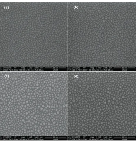
Figure 1. SEM images of four silver nanoparticle film samples with a 10 nm mass thickness deposited on 50 nm thick HfO2pre-coated
substrates, the last three of which were annealed at different temperatures for different durations: (a) not annealed, (b) annealed at 150◦
C for 2 min, (c) annealed at 300◦
C for 2 min, and (d) annealed at 300◦
C for 20 min.
harvesting devices can therefore substantially enhance their excitonic photogeneration process [12–14].
For plasmonic effects, silver nanoparticles have been made in a variety of ways to enhance the performance of thin film based optoelectronic devices. For example, Tseng et al have proposed a fast technique for making Ag nanostructures from AgOx thin film deposited on a glass substrate using a femtosecond laser, which can be applied over large areas [15]. Similarly, simple, low-cost, nucleated silver nanoparticles have been demonstrated to exhibit broadband absorption enhancement in thin film amorphous silicon solar cells [16]. In this paper, we employed silver nanoparticles that were engineered to tune the plasmonic absorption spectrum to enhance the electron–hole pair generation in the proximal CdTe NCs. This enhancement leads to increased sensitivity and a broadened operating spectral range of the LS-NS devices. Careful tailoring of the plasmonic absorption enables further optimized device performance. Therefore, integrating monolayer NC films with the silver nanoparticles offers great potential for a low-cost light-sensitive platform that is promising for UV/visible sensing.
2. Device preparation and characterization
To obtain localized plasmonic nanostructures, we deposited silver nanoparticles on 50 nm thick HfO2dielectric layers of
our LS-NS devices using a thermal evaporator at a reduced evaporation rate of 0.3 ˚A s−1 in a vacuum environment. As a result of the low evaporation rate together with small mass thickness, nanometer size islands of silver isolated from each other were obtained. After the evaporation, the samples were annealed at different temperatures and for different durations (150◦C for 2 min, 300◦C for 2 min, and 300◦C for 20 min) to further allow the silver nanoparticles to reorganize into desired morphologies. In this method, the four main parameters that determine the size and organization of the resulting silver nanoparticles include the evaporation rate, deposition thickness, annealing temperature, and annealing duration. During the process of developing these silver nanoparticles, different mass thicknesses and evaporation rates (not all presented here) have been systematically studied. The best results were achieved with a mass thickness of 10 nm at an evaporation rate of 0.3 ˚A s−1 as the optimal case, which gives the sharpest peak and the narrowest full-width at half-maximum (FWHM), in addition to the LSP resonance falling in the desired spectral range. Scanning electron microscopy (SEM) images of the four silver film samples deposited with a film mass thickness of 10 nm on the HfO2coated substrates and annealed at different temperatures
for different durations are shown in figure 1. Here it can be seen that the heat treatment helps the silver nanoparticles to reorganize themselves such that they become more isolated from each other and more spherical in shape.
Figure 2. (a) Optical excitation spectra of the silver nanoparticle films with a mass thickness of 10 nm deposited at 0.3 ˚A s−1evaporation
rate annealed at different temperatures for different durations. (b) Optical extinction spectra of a 10 nm thick silver nanoparticle film annealed at 300◦
C for 20 min covered with 1 nm thick Al2O3, a different number of PDDA and PSS bilayers (as indicated in the legend),
and a single monolayer of NCs.
The measured optical absorption spectra of the resulting silver nanoparticle films (given in figure2(a)) are consistent with their SEM images displayed in figure1. With annealing, the trend of obtaining a stronger, blue-shifted LSP resonance with a narrow FWHM is observed from the optical extinction spectra, confirming the isolation and size reduction of nanoparticles seen in the SEM images. Later we shall discuss how this tunability of the resonance peak enhances the device sensitivity in the range where the photosensitivity is low. To facilitate subsequent layer-by-layer assembly of NCs, a 1 nm thick negatively charged aluminum oxide (Al2O3) layer was
deposited using atomic layer deposition (ALD) onto the silver nanoparticle films, followed by the coating of bilayers of PDDA and PSS polyelectrolytes. These intermediate layers did not significantly shift the LSP resonance (as seen in figure2(b)).
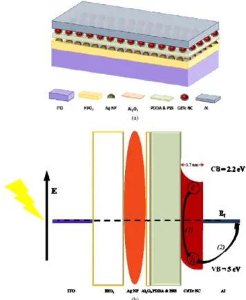
Figure 3(a) presents a sketch of the plasmonically enhanced LS-NS device, in which the aluminum oxide and polyelectrolyte polymers separate the silver nanoparticles and CdTe NCs. In this device architecture, charges are not allowed to pass directly through the device. Upon shining light on the device, excitons are dissociated at the aluminum and NC monolayer interface, mainly because of the difference between the workfunction of the NC monolayer [17] and that of the Al layer (see figure3(b)). Subsequently, holes are migrated and accumulated at the Al side due to the Al band alignment with respect to the NC monolayer. On the other hand, electrons tend to stay in the NCs because of the presence of the high dielectric layer of the HfO2film. Consequently,
holes start to accumulate at the Al contact, resulting in a positive potential buildup to the saturation point. Here the generation of photoinduced excitons over the Schottky barrier between the NC and Al electrode contributes to the increased photovoltage buildup. Furthermore, a higher voltage buildup is observed at shorter wavelengths. This spectral dependency stems form the larger number of states available for optical transitions with higher photon energy. This behavior is in strong agreement with the optical absorption spectrum of CdTe NCs. After a while, switching off the incident light
Figure 3. (a) Schematic illustration of a plasmonic light-sensitive nanocrystal skin (LS-NS). (b) Surface plasmon resonance sensitization of Ag nanoparticle and band alignment of CdTe NC (∼3.7 nm in size) conduction band (CB) and valence band (VB), and the workfunction (8) of Al and ITO. Ef demonstrates the Fermi level of CdTe NCs at equilibrium condition. Upon exciton
photogeneration (1), electrons tend to remain in the NCs while holes tend to migrate to the Al side (2).
results in a decreasing potential buildup. The device then exhibits a negative voltage due to the trapped electrons inside the NCs when there is no incident light. Moreover, the photovoltage building up as a result of the trapped electrons is directly related to the level of negative voltage observed
Nanotechnology 24 (2013) 155201 S Akhavan et al
after switching off the light. In other words, a larger potential buildup causes a higher negative voltage magnitude after turning the incident light off [7].
For the device implementation, ITO coated glasses were cleaned in Hellmanex, Milli-Q water, acetone, and isopropanol in an ultrasonic bath, which was continued by depositing a 50 nm thick HfO2 dielectric layer via ALD
on the ITO substrate. Then, 10 nm thick silver nanoparticle films were deposited on the dielectric layer at a very low evaporation rate of 0.3 ˚A s−1 in a vacuum environment. Subsequently, the films were annealed using rapid thermal annealing (RTA) at different temperatures and for different durations to modify and tune the LSP resonance peak. Here, the photosensitivity of these fabricated LS-NS devices was promoted by the localized plasmons excited in the metal nanoparticles and the modified density of photon states in the NCs at the proper spacing. Also, to make a spacer between the NCs and silver nanoparticles, 1 nm thick Al2O3was deposited
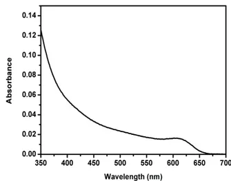
using ALD, followed by the layer-by-layer self-assembly of strong polyelectrolyte poly(diallyldimethylammonium chloride) (PDDA) and poly(sodium 4-styrenesulfonate) (PSS) bilayers via a fully computerized dip-coater system. Since the ALD uses pulses of water, hydrophilic surfaces were obtained with the ALD process, which further improves the self-assembly film quality [18]. The PDDA and PSS solutions were prepared by using a concentration of 2 mg ml−1 in 0.1 M NaCl solution. The PDDA − PSS films were coated by sequentially dipping the sample into the prepared solutions for 5 min, each time followed by rinsing the sample in water for 1 min. The thickness of the resulting PDDA − PSS bilayer is approximately 1.4 nm [19], as also measured by optical ellipsometry. After coating a final extra layer of positively charged PDDA on top of the alternating bilayers of positive–negative polyelectrolyte polymers (PDDA − PSS), negatively charged water-soluble CdTe NCs were coated. The sample was immersed in 4 mM CdTe NC dispersion for 20 min, and then again washed with water for 1 min to remove unbound CdTe NCs [20,21] and obtain a uniformly coated monolayer of CdTe NCs. Finally, an Al contact was deposited using the thermal evaporator on top of the NC layer. These aqueous CdTe NCs were synthesized based on the recipe given in [22]. The as-synthesized NCs are ∼3.7 nm in diameter, with the first exciton peak at around 605 nm, as depicted in figure4.
All optoelectronic characterizations were performed, without applying any external bias across the device, using an Agilent parameter analyzer and a Xenon light source with a monochromator as the excitation source. For wavelengths longer than 500 nm, a color glass filter, FSQ-GG 400 Newport (with a cut-off of 400 nm), was used to prevent mixing of the second harmonic. Optical power was measured using a Newport 1835C multi-function optical powermeter. During all measurements, the samples were connected in series with a load resistance of 200 M.
3. Results and discussions
The spacing between the plasmonic structures and semicon-ductor materials affect the level of plasmonic coupling and the
Figure 4. UV–vis absorption spectrum of aqueous CdTe NCs at room temperature.
resulting enhancement factor [23]. The investigated LS-NS devices rely on the exciton dissociation at the quantum dot and metal interface due to the difference in the workfunctions. The plasmonic enhancement in this device depends not only on plasmonically increased optical absorption but also on the sustained capability of dissociating excitons at the interface, which is critical for the overall performance of the photosensor response. This is because the presented plasmonic photosensors rely on the photogenerated voltage buildup, rather than the photogenerated charge collection out of the device. Also, the absorption needs to be increased in the quantum dots, and any other increased absorption without contributing to the photovoltage buildup would lead to an additional loss for the device performance. As a result, the plasmonic enhancement does not occur just by introducing the plasmonic particles into the structure; their spacing to quantum dot interface also needs to be tuned to observe a net enhancement.
Light-sensitive nanocrystal skins are capable of operating with only a single monolayer of nanocrystals as the active absorbing medium across which no external bias is applied. On the other hand, in common NC-based photodetector, where an external bias is typically applied to dissociate the photongenerated charges, the active region thickness is restricted to a few hundred nanometers due to the diffusion length and short carrier lifetimes. However, because of the close interaction between the NCs and metal contact in the LS-NS devices, a NC monolayer is sufficient and no external bias is required. As a result, in contrast to conventional photodetectors, which would enhance the sensitivity by increasing the current, this study demonstrates that one can enhance the sensitivity of the LS-NS devices by increasing the photovoltage buildup, even in those ranges where the charge accumulation seems to be so limited.
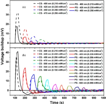
With plasmon coupling, while the field localization enhances the absorption, the spacing between the plasmonic structure and the active layer needs to be sufficiently thick to prevent the suppression of charge accumulation. For that, we designed our optimal device structure to minimize the
Figure 5. Voltage buildup of the LS-NS devices based on (a) four bilayers of PDDA − PSS and (b) seven bilayers of PDDA − PSS at different excitation wavelengths. In each set, the solid line
represents the plasmonic sample (PS) and the dashed line represents the control sample (CS).
effect of suppression and maximize the influence of NC absorption enhancement. For the localized plasmon coupling in the proximity of metallic nanostructures, we separated CdTe NCs and silver nanoparticles by a 1 nm thick Al2O3
film in addition to the bilayers of PDDA and PSS. Aluminum oxide film was set to be only 1 nm thick to have the minimum possible resonance red shift following the assembly of bilayers of PDDA and PSS and the monolayer of CdTe NCs using dip coating. A varying number of bilayers of PDDA and PSS were deposited on 1 nm Al2O3 as part
of the spacer between the metal nanoparticles and the semiconductor NCs to investigate the net effect of the LSP enhancement as a function of the spacing. Accordingly, we prepared three different sets of devices, each one having its own control sample (each of which is a bare structure where there is no plasmonic nanoparticle film incorporated). The reason for having individual control samples is the potential change in the surface coverage of the NCs as the number of polyelectrolyte bilayers changes [24, 25]. The dependence of optical absorption on the number of bilayers can directly affect the potential buildup and may enhance the photosensitivity of the device. The device sensitivity (S) is calculated by taking the ratio of the voltage buildup(V) and the incident optical power(P) impinging on the device, which is given by
S = V
P. (1)
The spacer between the plasmonic structure and NCs consists of 1 nm thick Al2O3, in addition to the varying
number of PDDA + PSS bilayers, and an extra positively
Figure 6. Comparison of the photosensitivity of LS-NS devices in the absence and presence of plasmonic nanostructures based on (a) four bilayers, (b) seven bilayers, and (c) ten bilayers of PDDA and PSS separating films. Inset figures present the sensitivity
enhancement factor.
charged PDDA layer for depositing negatively charged NCs. We begin with an approximately 7 nm thick spacer consisting of 1 nm Al2O3 and 4 bilayers of PDDA + PSS.
Comparing this plasmonically coupled device and its control sample shows the suppression of the voltage buildup and the consequent reduced level of the device sensitivity. Suppressing the voltage buildup can be explained by the reduced number of charges trapped inside NCs, which is directly related to the reduced storage of the holes at the Al contact. In the case that the separation distance is not enough or the NCs possibly contact with the metal nanoparticles, electrons are not completely trapped inside the NCs. Instead they can leak into the metal nanoparticles. Consequently, a smaller amount of charge is trapped inside the NCs, which results in a smaller voltage buildup (see figure 5(a)). In this case, the control sample has a signal output to yield a voltage buildup starting around 475 nm; however, the operational wavelength range is limited to 450 nm in the plasmonic structure due to the suppression of charge accumulation. Indeed, for the plasmonic structure beyond 450 nm, the voltage buildup level approaches the minimum noise equivalent intensity, which occurs after 475 nm for the control sample (see figure6(a)).
Increasing the spacing between the silver nanoparticles and the NCs from about 7 nm to about 11 nm (using 1 nm Al2O3 and 7 bilayers PDDA + PSS) leads to a great
enhancement. This improvement is basically attributed to the prevention of the charge accumulation suppression. In the presence of the metal nanoparticles, optical absorption of the CdTe NCs film is enhanced, which in turn increases the electron–hole generation. When the spacer layer is also sufficiently thick to prevent charge accumulation suppression of the NCs, electrons are trapped inside the NCs and
Nanotechnology 24 (2013) 155201 S Akhavan et al
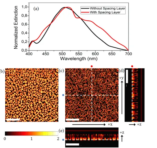
Figure 7. (a) Normalized extinction of the simulated silver nanoparticles with and without the presence of spacing layer. (b) Electric field intensity distribution at the interface of HfO2film and the silver nanoparticles. (c) Electric field distribution along the interface of the
spacing layer and air interface. (d) Cross-sectional 2D electric field intensity distribution along y–z plane. White dashed line coincides with the vertical line of figure7(c) indicated with red dots. (e) Cross-sectional 2D electric field intensity distribution along x–z plane. White dashed line coincides with the horizontal line of figure7(c) indicated with blue dots. All the color bars and scale bars are identical for the cross-sectional electric field maps. Scale bars correspond to 200 nm and the color bar represents relative values of electric field intensity ranging from 0 to 2 on a logarithmic scale.
holes get accumulated at the metal (Al) contact. As a result, a larger voltage buildup can be observed, which consequently enhances the sensitivity of the device (see figure 5(b)). Here we observed the sensitivity enhancement over a broad spectral range (400–525 nm), up to a maximum level of 2.6-fold, compared to the control sample. The plasmonic structure exhibits a significant enhancement in the sensitivity at around 525 nm, which also agrees well with the silver nanostructure LSP resonance peak (see the inset of figure6(b)). Furthermore, voltage buildup can be observed at longer wavelengths (up to 650 nm) for the plasmonic device compared to the control sample. In other words, at longer wavelengths, due to the low absorption of NCs, we observed a higher sensitivity enhancement with the plasmonic structure compared to the control sample. This evidence supports the absorption enhancement of CdTe NCs with plasmonic silver nanostructures, since NCs show very low absorption at long wavelengths.
Further increasing the interparticle spacer between the silver nanoparticles and the NCs to about 16 nm (using 1 nm Al2O3 together with 10 bilayers PDDA and PSS) to
prevent charge accumulation suppression again enhances the overall sensitivity and increases the operational wavelength
range, though not as much as the 11 nm case. However, a considerable enhancement can still be observed at around 525 nm as a result of the LSP of the silver nanostructures (figure 6(c)). Moreover, it can be realized that the control sample based on 10 bilayers of PDDA − PSS has a higher sensitivity level compared to the 7 bilayers because of the dependency of the voltage buildup on the number of bilayers. However, the plasmonic structure of 7 bilayers LS-NS is superior to both the control sample and the plasmonic sample of 10 bilayers in terms of the sensitivity around the LSP resonance (see figures 6(b)–(c)). It is evident in designing plasmonic LS-NS structures that placing a proper separator film between the NCs and plasmonic nanoparticles is one of the important factors that determine the level of plasmonic interactions.
To understand the underlying mechanism in the sensitivity enhancement of the LS-NS devices, we performed several numerical simulations and observed near-field electric field enhancement computed in the vicinity of the silver nanoparticles. We also compared the far-field extinction of the simulated nanoparticles with the experimental measurements. Figure7(a) shows the extinction response of the nanoparticles with and without the spacing layer, which can be compared
to figure 2. In general, our experimental and theoretical responses are found to be in agreement. The difference between the simulation results and the experimental response is attributed to the thickness variation of silver nanoparticles in three dimensions, background noise in the SEM image, other smaller particles that are not modeled effectively in the simulations, and limited simulation area compared to the real device surface. These effects lead to different resonant modes and resonance peak broadening in the extinction data.
Cross-sectional electric field intensity maps given at the special positions present the electric field intensity localization around the silver nanoparticles at the LSP resonance wavelength 520 nm. Figures 7(b)–(c) show the electric field intensity enhancements of the HfO2–silver
nanoparticle interface and the spacing layer–air interface, respectively, on a logarithmic scale. Figures7(d)–(e) depict the electric field intensity enhancements of the two surface normal cross-sectional maps at some random positions indicated with the dashed lines in figure7(c). In figure 7(c), even at 11 nm distance from the silver nanoparticles, we observe electric field intensity enhancement with a factor of slightly less than 10-fold. The observed locally enhanced electric field due to the resonance of silver nanoparticles supports that the excitation of the LSP in the silver nanoparticles is responsible for the absorption enhancement in the CdTe NCs, which in turn leads to increased electron–hole pair photogeneration.
Here the numerical simulations are run using commer-cially available software FDTD solver from Lumerical Inc. The simulated nanostructure was imported from the SEM image in figure 1(d) using the import picture property of the software. The RTA-annealed silver nanoparticles were considered to be 20 nm in thickness and a 31 nm thick dielectric layer encapsulating the silver nanoparticles was used, with a 11 nm additional separating layer on top of the silver nanoparticles. A 3D simulation region having 800 × 800 nm2 area with periodic boundary conditions was used since the random distribution of the particles imposes no additional periodicity effect on the plasmonic response. For simplicity, HfO2and indium tin oxide (ITO) layers under the
silver nanoparticles were taken as simple dielectric layers with an index of refraction of 1.95 and 7 bilayers of PDDA + PSS were modeled together as a single dielectric layer having a dielectric constant 1.4. To obtain unpolarized response, two sets of simulations with orthogonal source polarizations were performed and, subsequently, the electric field intensities and transmission values were obtained using the average value of the results of these two simulation sets. Based on the simulation results it can be suggested that the experimentally observed well-defined LSP resonance around 525 nm creates strongly localized electric field intensity enhancement at the position of the CdTe NCs.
4. Conclusion
In conclusion, to investigate the effect of localized plasmons in the vicinity of metallic nanostructures, we studied the
spacing-dependent photosensitivity of the LS-NS devices with metallic nanoparticles incorporated at varying separation distances to the NC skins. We demonstrated that, using LSP, the photosensitivity of NC monolayer light-sensitive skins can be enhanced or suppressed depending on the thickness of the separating film between the NCs and the metallic nanoparticles, and that their operating spectral range can be accordingly extended or curtailed across the region in which the NC optical absorption is not sufficient for charge generation. The measured voltage buildup spectra clearly reveal the net influence of the metallic nanoparticles on the combined effect of optical absorption enhancement and charge accumulation suppression in the LS-NS devices. The plasmonic nanostructure can also be tuned to enhance the photosensitivity of the resulting light-sensitive devices toward the infrared region if desired. These results may inspire new approaches towards the engineering of photosensitive NC-based devices.
Acknowledgments
We acknowledge the financial support in part by ESF EURYI, EU FP7 Nanophotonics4Energy NoE, and TUBITAK under the Project No. EEEAG 110E217, 111E189, and 112E183, and in part by NRF-CRP6-2010-02 and NRF RF 2009-09. KG acknowledges support from TUBITAK BIDEB and HVD gratefully acknowledges additional support from TUBA.
References
[1] Gaponenko S V 2010 Introduction to Nanophotonics (New York: Cambridge University Press) [2] Reiss P, Proti`ere M and Li L 2009 Small5 154–68
[3] Erdem T and Demir H V 2011 Nature Photon.5 126
[4] Demir H V, Nizamoglu S, Erdem T, Mutlugun E,
Gaponik N and Eychm¨uller A 2011 Nano Today6 632–47
[5] Konstantatos G, Howard I, Fischer A, Hoogland S, Clifford J, Klem E, Levina L and Sargent E H 2006 Nature442 180–3
[6] Konstantatos G and Sargent E H 2010 Nature Nanotechnol.
5 391–400
[7] Akhavan S, Guzelturk B, Sharma V K and Demir H V 2012 Opt. Express12 25255–66
[8] Dereniak E L and Boreman G D 1996 Infrared Detectors and Systems(New York: Wiley)
[9] Raether H 1988 Surface Plasmons (Berlin: Springer) [10] Atwater H A and Polman A 2010 Nature Mater.9 205–13
[11] Sundararajan S P, Grady N K, Mirin N and Halas N J 2008 Nano Lett.8 624–30
[12] Chen H M et al 2012 ACS Nano6 7362–72
[13] Ferry V E, Polman A and Atwater H A 2011 ACS Nano
5 10055–64
[14] Knight M W, Sobhani H, Nordlander P and Halas N J 2012 Science332 702–4
[15] Tseng M L et al 2012 ACS Nano6 5190–7
[16] Chen X, Jia B, Saha J K, Cai B, Stokes N, Qiao Q, Wang Y, Shi Z and Gu M 2012 Nano Lett.12 2187–92
[17] Jasieniak J, Califano M and Watkins S E 2011 ACS Nano
5 5888–902
[18] Likovich E M, Jaramillo R, Russell K J, Ramanathan S and Narayanamurti V 2011 Adv. Mater.23 4521–5
[19] Merhari L 2009 Hybrid Nanocomposites for Nanotechnology: Electronic, Optical, Magnetic and Biomedical Applications (New York: Springer)
Nanotechnology 24 (2013) 155201 S Akhavan et al
[20] Decher G 1997 Science277 1232–7
[21] Shavel A, Gaponik N and Eychm¨uller A 2005 Eur. J. Inorg. Chem.18 3613–23
[22] Rogach A L, Franzl T, Klar T A, Feldmann J, Gaponik N, Lesnyak V, Shavel A, Eychm¨uller A, Rakovich Y P and Donegan J F 2007 J. Phys. Chem. C111 14628–37
[23] Kulakovich O, Strekal N, Yaroshevich A, Maskevich S, Gaponenko S, Nabiev I, Woggon U and Artemyev M 2002 Nano Lett.2 1449–52
[24] Ostrander J W, Mamedov A A and Kotov N A 2001 J. Am. Chem. Soc.123 1101–10
[25] Shavel A, Gaponik N and Eychm¨uller A 2004 J. Phys. Chem. B108 5905–8