Mater. Res. Soc. Symp. Proc. Vol. 1337 © 2011 Materials Research Society DOI: 10.1557/opl.2011.976
Matrix Density Effect on Morphology of Germanium Nanocrystals Embedded in Silicon Dioxide Thin Films
Arif S. Alagoz1, 2, Mustafa F. Genisel3, 4, Steinar Foss5, Terje G. Finstad5, Rasit Turan2
1 Department of Applied Science, University of Arkansas at Little Rock, Little Rock, AR, U.S.A 2 Department of Physics, Middle East Technical University, Ankara, Turkey.
3 Department of Chemistry, Middle East Technical University, Ankara, Turkey. 4 Department of Chemistry, Bilkent University, Ankara, Turkey.
5 Department of Physics, University of Oslo, Oslo, Norway. ABSTRACT
Flash type electronic memories are the preferred format in code storage at complex programs running on fast processors and larger media files in portable electronics due to fast write/read operations, long rewrite life, high density and low cost of fabrication. Scaling limitations of top-down fabrication approaches can be overcome in next generation flash memories by replacing continuous floating gate with array of nanocrystals. Germanium (Ge) is a good candidate for nanocrystal based flash memories due its small band gap. In this work, we present effect of silicon dioxide (SiO2) host matrix density on Ge nanocrystals morphology. Low
density Ge+SiO2 layers are deposited between high density SiO2 layers by using off-angle
magnetron sputter deposition. After high temperature post-annealing, faceted and elongated Ge nanocrystals formation is observed in low density layers. Effects of Ge concentration and annealing temperature on nanocrystal morphology and mean size were investigated by using transmission electron microscopy. Positive correlation between stress development and nanocrystal size is observed at Raman spectroscopy measurements. We concluded that non-uniform stress distribution on nanocrystals during growth is responsible from faceted and elongated nanocrystal morphology.
INTRODUCTION
One of the main issues in information technology (IT) is the storage of digital
information. Nanocrystal based new generation flash memories are promising to follow Moore’s law and overcome scaling limitations with higher operation performance. Intensive researches have been focused especially on germanium nanocrystal [1-9] due to its fabrication compatibility with current complementary metal oxide semiconductor (CMOS) technology and small band gap, providing short writing/erasing and long retention time [2,3]. Ion implantation [4], chemical vapor deposition [5], laser ablation deposition [6] and magnetron sputter deposition [7-9] have been widely used techniques to fabricate germanium nanocrystals embedded in a various host matrix.
In this study, we fabricated germanium nanocrystals embedded in silicon dioxide host matrix by off-angle magnetron sputter deposition and high temperature post annealing. We sandwiched low density Ge+SiO2 layers between higher density SiO2 layers. After post
SiO2 matrix density are the critical parameters for nanocrystals’ mean size and morphology.
Raman spectroscopy measurements also showed correlation between stress formation and Ge nanocrystals size after annealing. Non-uniform matrix density is addressed as the main reason of non-uniform stress distribution on nanocrystals which in turn cause non-spherical nanocrystal forms.
EXPERIMENT
N-type Si (100) with 40 nm thermal oxide wafers were subjected to RCA I & II surface cleaning procedures. Samples were loaded to Vaksis nano-D 100 magnetron sputter deposition system and chamber pumped down to 7x10⁻⁷ Torr before each deposition. Periodic
Ge+SiO2/SiO2 thin films were deposited at room temperature by sputtering 3 inch diameter Ge
and SiO2 targets with Argon plasma. SiO2 and Ge targets were located at +25o and -25o off-angle
with substrate normal, respectively. Sputtering pressure was fixed at 3 mTorr during depositions. RF power applied to SiO2 target was fixed and Ge concentration of each layer was controlled by
DC power applied to the Ge target. Thicknesses of the films were controlled by monitoring thickness monitor and deposition time, details of process parameters are listed in Table 1. Samples were annealed in a fused quartz furnace at 600oC, 700oC, 750oC and 800oC
temperatures under vacuum (3.4x10⁻⁵ Torr) for 30 minutes to form Ge nanocrystals. After post
annealing, cross sectional transmission electron microscopy (TEM) measurements were performed in order to investigate nanocrystals’ size and morphology. Each Ge+SiO2/SiO2
periodic layer of multilayer sample was deposited on another set of substrates with the same deposition conditions and subjected to the same annealing conditions. Samples were named as Ge-L2, Ge-L3, Ge-L4 and Ge-L5 referring to each corresponding layer of multilayer sample (see Table 1). Raman spectroscopy measurements are conducted on these samples to analyze Ge crystallization and stress formation after annealing.
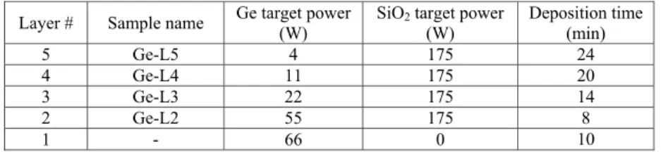
Table 1 Deposition parameters of multilayer and corresponding two layer samples Layer # Sample name Ge target power (W) SiO2 target power
(W) Deposition time (min)
5 Ge-L5 4 175 24
4 Ge-L4 11 175 20
3 Ge-L3 22 175 14
2 Ge-L2 55 175 8
1 - 66 0 10
Cross sectional transmission electron microscope measurements were carried out by analytical JEOL2000FX TEM at 200 keV. Backscattering Raman measurements were performed by Jobin Yvon Horiba confocal micro-Raman at room temperature. He-Ne laser (632.83 nm) was used as an excitation source, double monochromator and Peltier cooled CCD detector were used to detect Raman shifts.
DISCUSSION
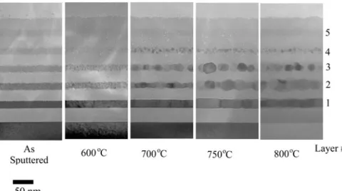
As shown in figure 1a, there is no indication of Ge nanocrystal formation in any layer of as-sputtered multilayer sample. After post annealing, layer 1 (%100 Ge) turns into a
polycrystalline thin film. Nanocrystal formation starts after annealing even at 600oC in layers 2,
3 and 4 as shown in figure 1b. Due to high Ge concentration in layer 2, nanocrystals’ size increases dramatically with increasing annealing temperature and even exceeds the co-sputtered layer thickness; in addition nanocrystals in this layer took faceted and elongated forms. In figure 1b-e, well separated nanocrystals can be observed in layer 3 after annealing. Mean nanocrystal size in this layer is comparable with deposited layer thickness and again non-spherical faceted and elongated nanocrystals observed. Well separated and uniformly distributed nanocrystals are observed in layer 4. In this layer, nanocrystals’ mean size increases smoothly with increasing annealing temperature and the size variation is smaller. On the other hand, no crystallization can be detected in layer 5 due to the low Ge concentration.
Figure 1 Cross sectional transmission electron microscope images of multilayer Ge+SiO2
as-sputtered and post-annealed samples at 600oC, 700oC, 750oC, 800oC for 30 min.
Non-uniform compressive stress on nanocrystals formed by SiO2 host matrix can be
addressed as the reason of faceted and elongated nanocrystal morphology [10]. ±25o off-angle
co-sputtering of Ge and SiO2 results in non-uniform low density film which causes non-uniform
stress after annealing. In layer 2 and 3, higher density SiO2 layers behaves as barriers during
nanocrystal growth, hence Ge nanocrystals preferentially elongate along co-sputtered layers. Correlation between Ge nanocrystal formation and stress built-up on nanocrystals were investigated by Raman spectroscopy in Ge-L2, Ge-L3, Ge-L4 and Ge-L5 samples. As expected, as-sputtered and Ge-L5 samples did not show any indication of nanocrystal formation due to low deposition temperature and low Ge concentration, respectively. Weak Ge-Ge transverse optical
(TO) Raman signal of Ge-L4 lost in the broad longitudinal optical (LO) peak of Si substrate centered at 301 cm-1 [11], therefore nanocrystal formation couldn’t observed. Figure 2a shows
Ge-Ge TO peak at 300 cm-1 after annealing of sample Ge-L3 at 600oC. Ge-Ge TO peak intensity
increases gradually at 700oC and 750oC then decreases at 800oC. Note that Si LO peak is fixed at
301 cm-1 while Ge TO signal shifts with increasing annealing temperature. Correlation of Ge-Ge TO peak position and nanocrystals’ mean size as a function of annealing temperature is shown in figure 2b.
(a) (b) Figure 2 Raman spectra of Ge-L3 for different annealing temperatures (a) and correlation
between Ge-Ge TO peak shift and mean nanocrystal size with changing post-annealing temperature.
It is know that Ge-Ge TO peak shift to high wavenumbers with increasing nanocrystal size due to phonon confinement effect [12, 13] and shift to low wavenumbers is due to the stress formation on the nanocrystals [14, 15]. Although, nanocrystal size increase and stress formation are coupled latter dominates in these samples. This strong relationship also confirms high compressive silicon dioxide host matrix stress induced on germanium nanocrystals. CONCLUSIONS
We fabricated germanium nanocrystals in low density Ge+SiO2 layer between higher
density SiO2 layers by using off-angle magnetron sputter deposition and high temperature post
annealing. We observed non-spherical and faceted Ge nanocrystals in low density Ge+SiO2
layers and attributed this effect to non-uniform compressive stress formation in non-uniform low density host matrix. We found that atomic Ge concentration, annealing temperature and SiO2
matrix density are the critical parameters for nanocrystals’ mean size and morphology. Raman spectroscopy confirmed germanium nanosrystal formation and high compressive silicon dioxide stress induced on germanium nanocrystals.
ACKNOWLEDGMENTS
This work has been partially supported by the EU FP6 projects SEMINANO under the Contract No. NMP4 CT2004 505285.
REFERENCES
1. H. I. Hanafi, S. Tiwari and I. Khan IEEE T. Electron Dev. 43 1553 (1996) 2. M. She and T. J. King IEEE T. Electron Dev. 50 1934 (2003)
3. V. Beyer, J. von Borany and M. Klimenkov J. Appl. Phys. 101 094507 (2007)
4. E. S. Marstein, A. E. Gunnæs, U. Serincan, S. Jørgensen, A. Olsen, R. Turan and T. G. Finstad Nucl. Instrum. Meth. B 207 424 (2003)
5. S. A÷an, A. Çelik-Aktas, J. M. Zuo, A. Dana and A. AydÕnlÕ Appl. Phys. A-Mater. 83 107 (2006)
6. W. L. Liu, P. F. Lee, J. Y. Dai, J. Wang, H. L. W. Chan, C. L. Choy, Z. T. Song and S. L. Feng Appl. Phys. Lett. 86 013110 (2005)
7. N. A. P. Mogaddam, A. S. Alagoz, S. Yerci, R. Turan, S. Foss and T. Finstad J. Appl. Phys., 104, 124309 (2008)
8. P. Basa, A. S. Alagoz, T. Lohner, M. Kulakci, R. Turan, K. Nagy and Zs. J. Horváth, App. Surf. Sci., 254, 3626 (2008)
9. A. Gencer Imer, S. Yerci, A. S. Alagoz, M. Kulakci, U. Serincan, T. G. Finstad and R. Turan J. of Nano. and Nanotech.10, 525 (2010)
10. A. V. Kolobov, S. Q. Wei, W. S. Yan, H. Oyanagi, Y. Maeda and K. Tanaka Phys. Rev. B 67 195314 (2003)
11. A. V. Kolobov J. Appl. Phys. 87 2926 (2000)
12. U. Serincan, G. Kartopu, A. Guennes, T. G. Finstad, R. Turan, Y. Ekinci and S. C. Bayliss Semicond. Sci. Tech. 19 247 (2004)
13. M. Fujii, S. Hayashi and K. Yamamoto Jpn. J. Appl. Phys. 30 687 (1991)
14. W. K. Choi, H. G. Chew, F. Zheng, W. K. Chim, Y. L. Foo and E. A. Fitzgerald E A Appl. Phys. Lett. 89 113126 (2006)
15. I. D. Sharp, D. O. Yi, Q. Xu, C. Y. Liao, J. W. Beeman, Z. Liliental-Weber, K. M. Yu, D. N. Zakharov, J. W. Ager III, D. C. Chrzan and E. E. Haller Appl. Phys. Lett. 86 063107 (2005)