Field-effect-assisted photoconductivity in PbS films deposited on silicon
dioxide
L. Pintilie, E. Pentia, I. Matei, I. Pintilie, and E. Ozbay
Citation: J. Appl. Phys. 91, 5782 (2002); doi: 10.1063/1.1468277 View online: http://dx.doi.org/10.1063/1.1468277
View Table of Contents: http://jap.aip.org/resource/1/JAPIAU/v91/i9
Published by the American Institute of Physics.
Additional information on J. Appl. Phys.
Journal Homepage: http://jap.aip.org/Journal Information: http://jap.aip.org/about/about_the_journal
Top downloads: http://jap.aip.org/features/most_downloaded
2700-nm-wavelength domain for different values and polarities of the drain and gate voltages. The best results were obtained for a positive gate, when both semiconductors are in depletion. An enhancement of about 25% of the photoconductive signal is obtained compared with the case when the gate electrode is absent or is not used. A simple model is proposed that explains the behavior of the dark current and photoconductive signal in PbS film with changing the gate voltage. © 2002 American Institute of Physics. 关DOI: 10.1063/1.1468277兴
I. INTRODUCTION
Lead sulfide共PbS兲 is a well-known A4B6semiconductor compound with very good photoconductive properties in the infrared共IR兲 domain 共800–3000 nm at room temperature兲.1,2 It has largely been used to manufacture photoconductive cells for civil and military applications. The standard method used for preparing PbS films is the chemical bath deposition 共CBD兲.3– 6 This method is less expensive, easy to handle, allowing the deposition of PbS films on a large area and on various substrates. The usual substrate for deposition is glass and electrical Ohmic contacts are made from vacuum-evaporated gold, in coplanar configuration. PbS films were also deposited on other semiconductor materials 共for ex-ample on Si, Ge, or InP兲,7,8on ferroelectrics ceramics共PZT type兲,9 or on dielectrics 关silicon nitride (Si3N4)兴.10 Pseudo-metal–oxide–semiconductor 共pseudo-MOS兲 structures were also manufactured in order to study the field-effect-assisted photoconductivity. An example is the PbS/Si3N4/Si structure in which the drain and source electrodes are deposited on the PbS surface and the gate electrode is on the Si substrate.10 The structure is p – i – n-type, PbS being the p-type semicon-ductor, while the Si substrate is n type. It was shown that on such structures it is possible to control the photoconductive signal in PbS by the applied gate voltage. For positive gate voltages it is possible to obtain an enhancement of the signal-to-noise ratio compared with the case when no gate electrode is used. However, it was observed that for positive drain the leakage current through the dielectric layer in-creases, leading to increased noise and decreased signal. The best results were obtained for negative drain and positive gate cases when both semiconductors are in depletion.
In the present article the dielectric layer is silicon diox-ide (SiO2). A pseudo-MOS structure is realized and it is
shown that significant variation of the photoconductive sig-nal can be obtained by field effect for both positive and nega-tive drain, on the entire sensitivity spectrum of PbS. A simple model is proposed in order to explain the experimental re-sults.
II. SAMPLE PREPARATION AND EXPERIMENTAL METHODS
The SiO2layer was grown on single-crystalline n-type Si wafers. Thermal oxidation at 850 °C was used, in an atmo-sphere containing oxygen and water vapors. The final thick-ness of the SiO2 layer was of about 250 nm. The PbS film was deposited by the CBD method, using lead nitrate 关Pb共NO3)2] as the Pb2⫹ion source and thioureea as the S2⫺ ion source.6,9 The deposition is performed in alkaline me-dium, using sodium hydroxide共NaOH兲, the starting solution pH being 11. Small amounts of a reducing agent 共hydroxil-amine chlorhidrate兲 and of a Bi salt are introduced in the bath in order to control the nucleation/growth process during the deposition of the PbS layer. It is known that the photo-conductive properties of PbS are strongly dependent on film morphology that, in turns, depends on the bath composition.6,11,12The PbS film is then photolitographic pro-cessed, leaving an area of 2.5⫻3.5 mm2. Gold electrodes are vacuum evaporated on the PbS surface, the final active area being of 1.5⫻1.5 mm2. After electrode deposition, the PbS films are aged at 80 °C for about 80 h in air. The final struc-ture is schematically presented in Fig. 1.
The photoconductive measurements were performed in modulated light, using the standard setup composed by a grating monochromator共model Spex270兲, a lock-in amplifier 共model SR830DSP兲, a dc voltage source 共model Grundig 300兲, an incandescent lamp as an IR source 共30 W nominal electric power兲, and a mechanical chopper 共model Ithaco 383A兲. A load resistance, with a value close to the dark re-a兲Electronic mail: [email protected]
5782
sistance of the PbS film 共usually a few hundreds k⍀兲, is series connected with PbS and is used to collect the photo-conductive signal 共see Fig. 1兲. For current–voltage (I – V) characteristics a Keithley electrometer, with a built-in dc voltage source 共model 6517A兲 was used. For field-effect-assisted photoconductive measurements an aluminum elec-trode was deposited on the Si substrate. This will be the so-called gate electrode by analogy with the pseudo-MOS transistors manufactured using silicon-on-insulator 共SOI兲 structures. In the present case the conductive channel is PbS, the drain and source electrodes are on the PbS surface, and the Si substrate is the gate electrode.
III. EXPERIMENTAL RESULTS
The transversal I – V characteristics, between one elec-trode from the PbS surface and the gate elecelec-trode, had shown that the leakage current through the dielectric layer is very low 共a few pA兲 no matter the polarity on the PbS surface. The drain I – V characteristics are represented in Fig. 2 for different polarities and values of the gate voltage. These measurements were performed keeping the sample in the dark, thus no light was applied on the surface of the PbS
film. It can be observed that the value of the drain current decreases by increasing the value of gate voltage Vg.
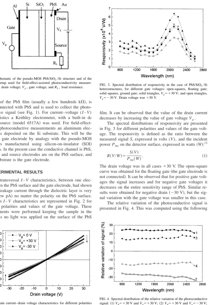
The spectral distributions of responsivity are presented in Fig. 3 for different polarities and values of the gate volt-age. The responsivity is defined as the ratio between the measured signal S, expressed in volts (V), and the incident power Pincon the detector surface, expressed in watts共W兲:13
R共V/W兲⫽ S共V兲
Pinc共W兲. 共1兲
The drain voltage was in all cases ⫹30 V. The open-square curve was obtained for the floating gate共the gate electrode is not connected兲. It can be observed that for positive gate volt-ages the signal increases and for negative gate voltvolt-ages it decreases on the entire sensitivity range of PbS. Similar re-sults were obtained for negative drain共⫺30 V兲, but the sig-nal variation with the gate voltage was smaller in this case.
The relative variation of the photoconductive signal is presented in Fig. 4. This was computed using the following
FIG. 1. Schematic of the pseudo-MOS PbS/SiO2/Si structure and of the
electrical setup used for field-effect-assisted photoconductivity measure-ments: Vd, drain voltage; Vg, gate voltage; and RL, load resistance.
FIG. 2. Drain current–drain voltage characteristics for different polarities and values of gate voltage Vg. Arrows show the increasing of the gate voltage Vg.
FIG. 3. Spectral distribution of responsivity in the case of PbS/SiO2/Si
heterostructures, for different gate voltages: open-squares, floating gate; solid squares, ground gate; solid triangles, Vg⫽⫹30 V; and open triangles, Vg⫽⫺30 V. Drain voltage was ⫹30 V.
FIG. 4. Spectral distribution of the relative variation of the photoconductive signal:共1兲 Vd⫽⫹30 V and Vg⫽⫹30 V; 共2兲 Vd⫽⫹30 V and Vg⫽⫺30 V;
共3兲 Vd⫽⫺30 V and Vg⫽⫹30 V; and 共4兲 Vd⫽⫺30 V and Vg⫽⫺30 V. Formula共2兲 was used for computation.
5783
formula:
⌬S共%兲⫽S共Vg兲⫺Sfloat
Sfloat
, 共2兲
where S(Vg) is the signal corresponding to a certain value of
the gate voltage Vgand Sfloatis the signal measured when the gate is floating 共is not connected兲. As it can be seen, the relative variation of the signal is almost constant on the PbS sensitivity range 共800–2600 nm, the cutoff wavelength is 2600 nm due to the glass bulb of the incandescent lamp, when using a Nernst glower the cutoff wavelength is 3000 nm兲.
The wavelength was then set to a fixed value共1000 and 2000 nm兲 and the dependence of the photoconductive signal on the gate voltage was raised. The obtained results are pre-sented in Fig. 5. The dependence is almost linear up to about Vg⫽15 V and then has the tendency to saturate. These curves were raised for a positive voltage of 30 V applied on the drain electrode.
IV. DISCUSSIONS AND THEORY
The signal variation with the gate voltage can be quali-tatively explained if the field effect is considered. As it is known, the chemically deposited PbS films are p type.1 Con-sidering that the Si substrate is n type, the studied samples are similar to p – i – n structures will be considered an ideal case, with an ideal insulator and flat energy bands for Vg
⫽0 V.
Two effects can lead to signal variation with the applied gate voltage.
A. Variation of depleted region width in the PbS film
A simple model can be developed in this case. Consid-ering positive Vg, it follows that holes will be rejected from
the PbS/SiO2 interface and depletion will occur. The PbS film can be divided in two layers in this case: one is the space-charge region, near the PbS/SiO2 interface, which is supposedly free of charge carriers; the second one is the neutral region. The model supposes that no current will flow through the space-charge region. Thus, the current flows only through the neutral channel. It is supposed that the thickness
of this channel is constant between the drain and source elec-trodes. This is valid when load resistance RL 共see Fig. 1兲 is
larger than the PbS film’s dark resistance. A value of 1 M⍀ was considered for RL, larger than the value of 250 k⍀ that
is typical for PbS films. However, the value for RL used in
simulation is larger than that used in the measurements, thus some simulated quantities will be smaller than the measured ones 共for example, the dark current兲. The formula that gives the dark current value is
I⫽ Vd RL⫹ L l共d⫺xPbS兲 ⫽ Vd RL⫹ 共d⫺xPbS兲 , 共3兲
where Vdis the drain voltage,is the PbS resistivity, L is the
distance between the drain and source electrodes, l is the width of these electrodes, d is the thickness of the PbS film, and xPbSis the thickness of the space-charge region in PbS. For the sake of simplicity it was considered that L⫽1 共the distance between the PbS electrodes is equal with their width兲. The thickness of the space-charge region in PbS can be computed solving Poisson’s equation in a simplified struc-ture like that from Fig. 6. Thus, solving the Poisson’s equa-tion in the three materials with the appropriate boundary and continuity conditions, and taking into account that14
Vg⫹⌽PbS⫹Vi⫹⌽Si⫽0,
共4兲
xPbSNA⫽xSiND,
the following expression for xPbSwill result:
xPbS⫽ ⫺di⫹
冑
di 2⫹ 2⑀i 2 qNA冉
1 ⑀PbS ⫹⑀1 Si NA ND冊
共V g⫹Vox兲 ⑀i 2冉
1 ⑀PbS⫹ 1 ⑀Si NA ND冊
. 共5兲 In Eq.共4兲 the first equation expresses the potential continuity at x⫽d⫹di⫹xSi 共the border between the Si space charge and the Si neutral volume兲. The second equation expresses the charge conservation 共the charges in the two depleted re-gions have to be equal兲. The notations are Vgis the positivevoltage applied on the gate to obtain depletion, ⌽PbS is the surface potential at the PbS/SiO2 interface (x⫽d), Vi is the
voltage drop across the insulator, and⌽Siis the surface
po-FIG. 5. Dependence of the photoconductive signal on the gate voltage (Vd⫽⫹30 V).
tential at the Si/SiO2 interface (x⫽d⫹di). In Eq. 共5兲 the
notations are ⑀PbSis the dielectric constant of PbS共175兲, ⑀i dielectric constant of insulator 共in case of SiO2 is 4兲, ⑀Si dielectric constant of Si共12兲, NA is the acceptor concentra-tion in PbS (1016– 1017cm⫺3), N
D the donor concentration
in Si共around 1015cm⫺3兲, and q is the elementary charge. Vox is a positive voltage that takes into consideration the pres-ence of the positive charge in the SiO2 layer. Due to this charge the structure is depleted when negative gate voltages are applied, as it can be seen from the capacitance–voltage (C – V) characteristics presented in Fig. 7. The value of Vox can be as high as a few tenth of volts. We have considered a value of 30 V for further simulation.
From Eq. 共5兲 it can be observed that increasing Vg the
thickness of the space-charge region in PbS increases. The thickness of the neutral channel, that is, d⫺xPbS, decreases, the resistance of this channel increases, and the current flow-ing through the PbS film decreases with Vg. This is shown in
Fig. 8 and is confirmed by the experimental data presented in Fig. 2.
The amplitude of the photoconductive signal, in the case of the rectangular modulation of the incident light, is given by ⌬v⫽ RLVd
冉
RL⫹ d⫺xPbS冊
2 ⌬ 2 1 d⫺xPbS⬘
, 共6兲where⌬ is the electric conductivity’s variation of the PbS film when it is exposed to light, is the dark electric con-ductivity of PbS film, xPbS is the thickness of space-charge region in PbS in the dark condition, and xPbS
⬘
is the thickness of the space-charge region in PbS when the film is exposed to light. Formula 共6兲 was derived considering that the thick-ness of the neutral conductive channel is constant. As was mentioned above, this is valid only if the load resistance RL is much larger than the value of the PbS dark resistance. The usual value of the dark electric conductivity for PbS is about 1.5⫻10⫺1⍀⫺1cm⫺1. It will be considered that the electric conductivity variation ⌬ is the same no matter if the gate voltage is applied or not and is given only by the variation of the charge-carrier concentration and carrier mobility under illumination. Variation of the charge-carrier concentration under illumination changes the thickness of the space-charge region, also. This is considered through xPbS⬘
, which is com-puted using a carrier concentration equal with NA⫹nIin-stead NA, where nI is the concentration of photogenerated
carriers. This is of the order of 1014– 1015cm⫺3 共depending on the light intensity兲, while NA is of the order of at least
(5 – 10)⫻1016cm⫺3.
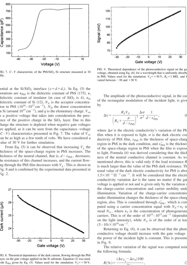
Returning to Eq. 共6兲, it can be observed that the photo-conductive voltage should increase with the gate voltage if the power of the incident light is constant. This is presented in Fig. 9.
The relative variation of the signal was computed using the following formula:
R共%兲⫽共⌬v
Vg⫺⌬v0兲100
⌬v0 , 共7兲
FIG. 7. C – V characteristic of the PbS/SiO2/Si structure measured at 10
kHz.
FIG. 8. Theoretical dependence of the dark current, flowing through the PbS layer, on the gate voltage applied on the Si substrate. Equation共3兲 was used, with XPbSgiven by Eq.共5兲. Values used for the simulation: Vd⫽⫹30 V, RL⫽1 M⍀, and Vgvaried between⫺30 and ⫹30 V.
FIG. 9. Theoretical dependence of the photoconductive signal on the gate voltage, obtained using Eq.共6兲, for a wavelength that is uniformly absorbed in PbS. Values used for the simulation: Vd⫽⫹30 V, RL⫽1 M⍀, and Vg varied between⫺30 and ⫹30 V.
5785
PbS/SiO2interface, their lifetime will decrease and the signal will be smaller. This effect seems to contribute also to the signal variation, mainly in the extreme cases when both in-terfaces are in inversion 共electron attracted in PbS, signal increases兲 or in accumulation 共holes attracted in PbS, signal decreases兲. It cannot explain, alone, the large signal variation observed in Fig. 5, but can explain why the signal has the tendency to saturate at high gate voltages共inversion兲. If Vgis
very large and the PbS/SiO2 interface is definitely in inver-sion or accumulation, a further increase of Vg will have no
effect because the negative or the positive charge already present at the interface will screen its influence.
V. CONCLUSIONS
Pseudo-MOS structures were manufactured using com-plex PbS/SiO2/Si structures. Field-effect-assisted photocon-ductivity in the PbS layer was investigated and the following conclusions were drawn:
共i兲 A signal variation of up to 50% can be obtained for positive drain and for gate voltage variation between ⫺30 and ⫹30 V.
共ii兲 An increase of the signal with 25% can be obtained for positive voltage.
共iii兲 Two possible effects can contribute to signal varia-tion:共1兲 the variation of the depletion width region in PbS with the gate voltage, and共2兲 the variation of the majority carrier共hole兲 lifetime with the gate voltage.
ACKNOWLEDGMENTS
This study was financially supported by NATO, through SfP Project No. 971970-INOWATE, and by the Romanian Ministry of Education and Research through Contract No. 1/2000.
1
G. H. Blount, P. J. Schreiber, and D. Smith, J. Appl. Phys. 44, 978共1973兲.
2
S. Espevik, C. Wu, and R. H. Bube, J. Appl. Phys. 42, 3513共1971兲.
3F. Kicinski, Chem. Ind. 4, 54共1948兲.
4P. A. Bu¨ger, O. G. Malan, and O. A. Kunze, Z. Naturforsch. A 26A, 1995 共1971兲.
5
K. L. Chopra and S. R. Das, Thin Films Solar Cells共Plenum, New York, 1983兲, p. 77.
6E. Pentia, L. Pintilie, C. Tivarus, I. Pintilie, and T. Botila, Mater. Sci. Eng.
B 80, 23共2001兲.
7
O. A. Gudaev, V. K. Malinovsky, and E. E. Paul, Thin Solid Films 198, 35
共1991兲.
8M. Isshiki, T. Endo, and K. Masumoto, J. Electrochem. Soc. 137, 2697 共1990兲.
9I. Pintilie, E. Pentia, L. Pintilie, D. Petre, T. Botila, and C. Constantin, J.
Appl. Phys. 78, 1713共1995兲.
10L. Pintilie, E. Pentia, I. Pintilie, and T. Botila, Appl. Phys. Lett. 76, 1890 共2000兲.
11V. M. Simic and Z. B. Marinkovic, Infrared Phys. 8, 189共1968兲. 12C. Nascu, V. Vomir, V. Ionescu, and I. Pop, Rev. Roum. Chem. 40, 127
共1995兲.
13Hamamatsu Infrared Detectors共Hamamatsu Photonics, Hamamatsu City,
Japan, 2000兲 Cat. No. KIRD 0001E07.
14C. Ravariu, A. Rusu, D. Dobrescu, F. Ravariu, and L. Dobrescu,