First-principles study of two- and one-dimensional honeycomb structures of boron nitride
M. Topsakal,1E. Aktürk,1and S. Ciraci1,2,
*
1UNAM-Institute of Materials Science and Nanotechnology, Bilkent University, Ankara 06800, Turkey 2Department of Physics, Bilkent University, Ankara 06800, Turkey
共Received 22 December 2008; revised manuscript received 12 February 2009; published 30 March 2009兲
This paper presents a systematic study of two- and one-dimensional honeycomb structures of boron nitride 共BN兲 using first-principles plane-wave method. In order to reveal dimensionality effects, a brief study of all allotropic forms of three-dimensional共3D兲 BN crystals and truly one-dimensional atomic BN chains are also included. Two-dimensional 共2D兲 graphenelike BN is a wide band-gap semiconductor with ionic bonding through significant charge transfer from B to N. Phonon-dispersion curves demonstrate the stability of 2D BN flakes. Quasi-one-dimensional 共1D兲 armchair BN nanoribbons are nonmagnetic semiconductors with edge states. Upon passivation of B and N with hydrogen atoms these edge states disappear and the band gap increases. Bare zigzag BN nanoribbons are metallic but become a ferromagnetic semiconductor when both their edges are passivated with hydrogen. However, their magnetic ground state, electronic band structure, and band gap are found to be strongly dependent on whether B or N edge of the ribbon is saturated with hydrogen. Vacancy defects in armchair and zigzag nanoribbons affect also the magnetic state and electronic structure. Harmonic, anharmonic, and plastic regions are deduced in the variation in the total energy of armchair and zigzag nanoribbons as a function of strain. The calculated force constants display a Hookian behavior. In the plastic region the nanoribbon is stretched, whereby the honeycomb structure of hexagons change into different polygons through sequential structural transformations. In order to reveal dimensionality effects these proper-ties are contrasted with those of various 3D BN crystals and 1D BN atomic chain.
DOI:10.1103/PhysRevB.79.115442 PACS number共s兲: 81.05.Uw, 73.22.⫺f, 75.75.⫹a, 63.22.⫺m I. INTRODUCTION
Synthesis of a single atomic plane of graphite, i.e.,
graphene with covalently bonded honeycomb lattice, has
been a breakthrough for several reasons.1–3 First, electrons behaving as if massless Dirac fermions have made the obser-vation of several relativistic effects possible. Second, stable graphene has disproved previous theories, which were con-cluded that two-dimensional 共2D兲 structures cannot be stable. Graphene displaying exceptional properties, such as high mobility even at room temperature, ambipolar effect, Klein tunneling, anomalous quantum hall effect, etc., seems to offer novel applications in various fields.4 Not only 2D graphene but also its quasi-one-dimensional 共1D兲 forms, such as armchair and zigzag nanoribbons, have shown novel electronic and magnetic properties,5–7which can lead to im-portant applications in nanotechnology. As a result, 2D hon-eycomb structures derived from group IV elements and group III-V and II-VI compounds are currently generating significant interest owing to their unique properties.
Boron nitride 共BN兲 in ionic honeycomb lattice which is the group III-V analog of graphene has also been produced having desired insulator characteristics.8 Nanosheets,9,10 nanocones,11 nanotubes,12 nanohorns,13 nanorods,14 and nanowires15of BN have already been synthesized, and these systems might hold promise for novel technological applica-tions. Among all these different structures, BN nanoribbons 共BNNRs兲, where the charge carriers are confined in two di-mensions and free to move in the third direction, are particu-larly important due to their well-defined geometry and pos-sible ease of manipulation.
BN nanoribbons posses different electronic and magnetic properties depending on their size and edge termination. Re-cently, the variation in band gaps of BN nanoribbons with their widths and Stark effect due to applied electric field have
been studied.16,17Recently the magnetic properties of zigzag BN nanoribbons 共ZBNNRs兲 have been investigated.18 Half-metallic properties have been revealed from these studies which might be important for spintronic applications. Pro-duction of graphene nanoribbons as small as 10 nm in width has been achieved19,20and similar techniques are expected to be developed for BN nanoribbons.
A thorough understanding of 2D BN honeycomb structure and their various nanoribbons is important for further study of this graphenelike compounds. BN by itself provides very interesting chemical and physical properties, which may lead to important applications. In this paper, we present a detailed
ab initio study of electronic, magnetic, and elastic properties
of 2D 共graphenelike兲 BN and bare and hydrogen-passivated quasi-1D BNNRs. We also investigated the effect of the va-cancy defects on these properties. To reveal the dimension-ality effects we include also a short discussion regarding three-dimensional共3D兲 BN bulk crystals and 1D BN atomic chains. We found that 2D BN is a nonmagnetic wide band-gap semiconductor. The ionic bonding due to a significant amount of charge from B to N atom opens a gap and hence dominates electronic structure. Calculated phonon-dispersion curves provide a clear evidence that 2D BN flakes are stable. The armchair and zigzag nanoribbons of BN display even more interesting electronic and magnetic properties. Bare and hydrogen-passivated armchair BN nanoribbons 共ABN-NRs兲 are nonmagnetic wide band-gap semiconductor. The value of the band gap of ABNNR having a width of w ⬎10 Å is practically independent from the width of nanor-ibbons. While the bare ZBNNRs are ferromagnetic metal, they become nonmagnetic semiconductor upon the passiva-tion of both edges. We found that 2D BN and its nanoribbons have properties that are complementary to graphene.
II. MODEL AND METHODOLOGY
We have performed first-principles plane-wave calcula-tions within density-functional theory共DFT兲 using projector augmented wave 共PAW兲 potentials.21 The exchange-correlation potential has been approximated by generalized gradient approximation 共GGA兲 using the PW91 共Ref. 22兲
functional both for spin-polarized and spin-unpolarized cases. All structures have been treated within supercell ge-ometry using the periodic boundary conditions. A plane-wave basis set with kinetic-energy cutoff of 500 eV has been used. In the self-consistent potential and total-energy calcu-lations the Brillouin zone 共BZ兲 is sampled by special k points. The numbers of these k points are共15⫻15⫻15兲 for bulk BN, 共25⫻25⫻1兲 for 2D BN, and 共25⫻1⫻1兲 for na-noribbons, respectively, and are scaled according to the size of superlattices. All atomic positions and lattice constants are optimized by using the conjugate gradient method, where the total energy and atomic forces are minimized. The conver-gence for energy is chosen as 10−5 eV between two steps, and the maximum Hellmann-Feynman forces acting on each atom is less than 0.02 eV/Å upon ionic relaxation. A large spacing of ⬃10 Å between monolayers and ⬃13 Å be-tween edges of two ribbons in adjacent supercells have been taken to prevent interactions between them. The pseudopo-tentials having three and five valence electrons for the B共B: 2s22p1兲 and N ions 共N: 2s22p3兲 were used. Numerical calcu-lations have been performed by using theVASPpackage.23,24 The phonon-dispersion curves are calculated within density-functional perturbation theory 共DFPT兲 using plane-wave methods as implemented in thePWSCF software.25
III. 3D BN CRYSTALS AND 1D ATOMIC CHAIN
In this section, we present our theoretical calculations on 3D bulk BN crystals and truly 1D BN atomic chain. Earlier these 3D bulk crystals26–30and 1D atomic chains31have been studied theoretically by using different methods. Our purpose in including these crystals of BN in different dimensionali-ties is to contrast their properdimensionali-ties with those of 2D and quasi-1D honeycomb structures of BN and also reveal di-mensionality effects.
A. 3D bulk BN crystals
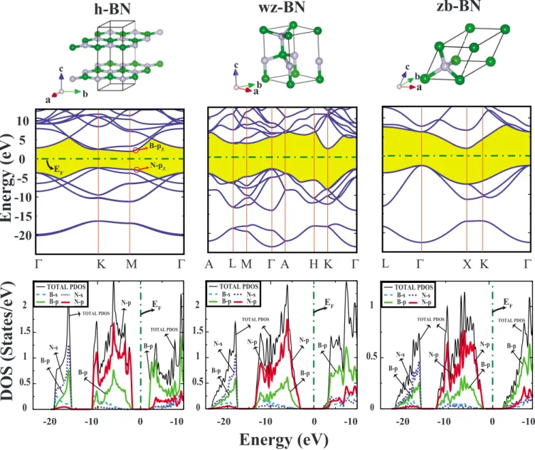
Three-dimensional bulk crystals include hexagonal-layered BN 共h-BN兲, wurtzite BN 共wz-BN兲, and zinc-blende BN 共zb-BN兲 structures. Their atomic configurations and primitive unit cells are described in Fig. 1. By using the expression
EC= E关BN兴 − E关B兴 − E关N兴, 共1兲
where E关BN兴 is the total energy per B-N pair of the opti-mized structure of BN crystal and E关B兴 and E关N兴 are the total energies of free B and N atoms, we calculated the equi-librium cohesive energies of h-BN, wz-BN, and zb-BN crys-tals as −17.65, −17.45, and −17.49 eV per B-N pair, respec-tively. Accordingly, h-BN, which is the analog of graphite, is the most energetic bulk structure. On the other hand, the
cubic BN structure is known to be the second hardest mate-rial of all.
The lattice constants of the optimized structures in equi-librium are a = 2.511 Å, c/a=2.66, and the distance between the nearest B and N atoms is d = 1.450 Å for h-BN layered crystal. For wz BN, optimized values of a, c/a, and d are calculated to be 2.542 Å, 1.64, and 1.561 Å, respectively. The zinc-blende structure has a lattice constant a = 2.561 Å and d = 1.568 Å. All our results related with the structural parameters are in good agreement with the experimental and theoretical values26–29,32 within the average error of ⬃1% 共TableI兲.
The calculated electronic band structure and total and par-tial共or orbital projected兲 density of states 共DOS兲 of 3D crys-tals are presented in Fig.1. These h-BN, wz-BN, and zb-BN crystals are indirect band-gap semiconductors with calcu-lated band gaps being EG= 4.47, 5.72, and 4.50 eV,
respec-tively. The calculated values of EG differ from the earlier
ones depending on the method used.33For h-BN having 2D BN atomic layers in the 共x,y兲 plane, the band structure is composed from the band structures of these individual atomic layers with hexagonal symmetry, which are slightly split due to weak coupling between them. The highest va-lence band has N-pzcharacter; the states of the lowest
con-duction band is formed from B-pz orbitals 共the z direction
corresponds to “c” in Fig.1兲. The overall features of the total
density of states 共TDOS兲 are similar for three 3D crystal structures. Valence band consists of two parts separated by a wide intraband gap. The lower part at⬃−20 eV is projected mainly to N-s and partly to N-p and B-s orbitals. The upper part is due to mainly N-p and partly B-p orbitals and has similarities in both zb-BN and wz-BN crystals. As for the lower part of the conduction band it is derived mainly from B-p orbitals. The differences of three 3D crystals are pro-nounced in the lower part of the conduction band.
We calculate the amount of charge on constituent B and N atoms in 3D crystals by performing the Löwdin34analysis in terms of the projection of plane waves into atomic orbitals. By subtracting the valencies of free B and N atoms from the calculated charge values on the same atoms in 3D crystals, we obtain the charge transfer,⌬Q. The calculated values of ⌬Q for h-BN, wz BN, and zb BN are 0.416, 0.342, and 0.334 electrons, respectively. The ⌬Q of zb BN and wz BN have almost equal values but the ⌬Q of h-BN crystal is signifi-cantly larger related to the shorter B-N bond length in h-BN crystal.
B. 1D BN atomic chain
BN forms stable segments of linear atomic chain31such as carbon.35This situation is in contrast to the second and third row elements共such as Si and Ge兲 and III-V compounds and metals 共such as Al, Au, etc.兲 which can form stable zigzag chain structures instead of linear-chain structures. Our results on optimized chain structure yield the cohesive energy EC
= 16.04 eV per B-N pair, the B-N distance d = 1.307 Å, the indirect band gap EG= 3.99 eV, and charge transfer from B
to N, ⌬Q=0.511 electrons. Hence the double bond between B and N is ionic.
IV. 2D HONEYCOMB STRUCTURE OF BN
Having discussed the overall structural and elastic prop-erties of 3D and 1D BNs, we now consider 2D BN with
hexagonal symmetry. The atomic structure of 2D BN is simi-lar to the honeycomb structure of graphene, except that the constituent atoms of the former are from III and V columns
-20
-15
-10
-5
0
5
10
Energy
(eV
)
h-BN
Γ
Κ
Μ
Γ
a b c EFΓ
Α
L
Μ
Γ
Η Κ
wz-BN
Α
ab czb-BN
Γ
X Κ
Γ
a b c B-pZ N-pZL
0 0.5 1 1.5 2 -20 -10 0 0 0.5 1 1.5 2 0 0.5 1DOS
(States/eV)
N-s TOTAL PDOS B-s B-p N-sN-p EF EF EF -10 -20 -10 0 -10 -20 -10 0 -10Energy (eV)
B-p N-p TOTAL PDOS B-s B-p N-sN-p TOTAL PDOS B-s B-p N-sN-p TOTAL PDOS TOTAL PDOS B-p B-p B-p N-s TOTAL PDOS N-p B-p N-p B-p TOTAL PDOS N-s B-p N-p B-p N-p TOTAL PDOS B-pFIG. 1.共Color online兲 Optimized atomic structure, energy bands, total 共TDOS兲, and orbital projected density of states 共PDOS兲 of various 3D crystals of BN.共a兲 Hexagonal 共h-BN兲 whose B共N兲 atoms are on top of the N共B兲 atoms in the consecutive layer; 共b兲 wurtzite 共wz-BN兲; and 共c兲 zinc-blende 共zb-BN兲 crystals. Dark-green and light-gray balls represent B and N atoms, respectively. The band gaps between conduction and valence bands are highlighted. The orbital character of states is indicated for the conduction and valence band edges. The zero of energy is set to the Fermi energy EF. All structures are fully optimized.
TABLE I. Values of the bond length d in Å, cohesive energy ECin eV per B-N pair, band gap EGin eV, charge transfer from B to N共⌬Q兲 in electrons, and lattice constants 共a and c兲 in Å calculated for various allotropic forms of BN in different dimensionality.
d EC EG ⌬Q Lattice 1D Chain 1.307 −16.04 3.99 0.511 a = 2.614 2D BN 1.452 −17.65 4.64 0.429 a = 2.511 h-BN 1.450 −17.65 4.47 0.416 a = 2.511, c/a=2.66 Wurtzite 1.561 −17.45 5.726 0.342 a = 2.542, c/a=1.63 Zinc blende 1.568 −17.49 4.50 0.334 a = 2.561
of the Periodic Table. Normally, the bond between nearest B and N atoms is formed from the bonding combination of B-sp2 and N-sp2 orbitals. However, owing to the electrone-gativity difference between B and N atoms, electrons are transferred from B to N. As a result, in contrast to purely covalent bond in graphene the bonding between B and N gains an ionic character. The charge transfer from B to N dominates several properties of 2D BN including the open-ing of the band gap. In this respect the BN honeycomb struc-ture is complementary to graphene.
A. Charge-density analysis and electronic structure
The atomic structure, atomic charge, charge transfer from B to N, and the electronic structure of 2D BN are presented in Fig.2. Contour plots of total charge indicate high density around N atoms. The difference charge density is calculated by subtracting charge densities of free B and N atoms from
the charge density of 2D BN, i.e., ⌬=BN−B−N. High-density contour plots around N atoms protruding toward the B-N bonds indicate charge transfer from B to N atoms. This way the B-N bonds achieve an ionic character. The amount of transfer of charge is calculated by Löwdin analysis to be ⌬Q=0.429 electrons. Interestingly, ⌬Q is slightly larger than that calculated for h-BN but significantly larger than those calculated for wz-BN and zb-BN crystals.
2D BN is a semiconductor. Calculated electronic energy bands are similar to those calculated for h-BN crystal. The andⴱbands of graphene which cross at the K and Kⴱpoints of the BZ open a gap in the 2D BN as bonding and antibond-ing combinations of N-pzand B-pzorbitals. The contribution
of N-pz is pronounced for the filled band at the edge of
valence band. The calculated band gap is indirect and EG
= 4.64 eV. TDOS and partial density of states show also similarity to those of the h-BN layered crystal presented in Fig.1.
B. Phonon spectrum
Even if the structure optimization resulting in the honey-comb structure in Fig.2can be taken as an indication for the stability of 2D BN, calculation of phonon-dispersion curves through the diagonalization of dynamical matrix provides a more stringent test for stability. One of the acoustical branches for⌫ to K curves taking a negative value even at a small region of BZ indicates the instability of the structure. There have been a number of experimental36and theoretical studies of phonon spectrum of 2D共Ref. 37兲 and 3D
honey-comb BN.38–42Here, the phonon-dispersion curves of h-BN, 2D BN, and 1D BN chain and density of states together with the infrared共IR兲 and Raman 共R兲 active modes of 2D BN and h-BN at ⌫ point have been calculated by using DFPT as implemented in thePWSCFsoftware.25For the DFPT phonon calculation of bulk h-BN, we used a four-atom primitive cell, which yield 12 phonon branches at the center of BZ in Fig.
3共a兲. The symmetry point group is calculated as D6h共space group P6/mmm兲. The irreducible representations at ⌫ is 2E2g+ 2B2g+ 2A2u+ 2E1u. While the modes E1u and E2g are doubly degenerate, B2g and A2u are nondegenerate. The modes E1uand A2u are IR active, the E2g is Raman active.
B2g is an inactive mode. Our results are in agreement with the previously calculated and experimental data but differ slightly from those of Serrano et al.40 While the present GGA calculations predict the B2gmode as an inactive mode, local-density approximation 共LDA兲 calculations by Serrano
et al. found B1g as an inactive mode. Most of the phonon bands of h-BN are degenerate. This indicates that the cou-pling between BN layers in h-BN is weak. However, it is well known that the BN is a polar material with long-range dipole-dipole interaction. This gives rise to the splitting be-tween longitudinal optical 共LO兲 and transverse optical 共TO兲 modes at the⌫ point. The lowest transverse acoustical 共TA兲 mode has parabolic dispersion as k→0, owing to rapidly decaying interatomic forces for transversal displacements.43 Another feature is the overlap of the lowest transversal opti-cal mode with the acoustiopti-cal modes.
In Fig.3共b兲we show the phonon-dispersion curve of BN atomic chain. Two TA modes have low frequency and get
FIG. 2. 共Color online兲 共a兲 Primitive unit cell of the honeycomb structure of 2D BN together with Bravais lattice vectors. Calculated total charge densityBNand difference charge density⌬ are also shown in the same panel.共b兲 Calculated electronic structure of 2D BN honeycomb crystal together with total, TDOS, and partial den-sity of states, PDOS, on B and N atoms. The orbital character of the states is also indicated.
very small but negative values near the zone center. This indicates structural instability as→⬁. However, the linear segments of BN atomic chain can be stable. Similar to h-BN, the doubly-degenerate TO branch overlaps with the LO branch.
For 2D BN honeycomb structure, the unit cell consists of two atoms. Accordingly, there are three acoustical and three optical branches in Fig. 3共c兲. The symmetry point group is
D3h关space group 共P-62m兲兴. Optical phonon modes at the ⌫
point is given by A2
⬙
+ 2E⬘
. The mode A2⬙
is IR active and theE
⬘
mode is both IR and Raman active. The similarity be-tween calculated phonon-dispersion curves of h-BN and 2D-BN is remarkable.We also calculate the phonon-dispersion curves of 2D BN honeycomb structure by using PAW potentials21 as imple-mented inVASP共Ref. 23兲 for further checking of the results
of our phonon calculation. Force constants are determined from the共8⫻8⫻1兲 supercells. The phonon modes were cal-culated by using the direct method as implemented in the PHON共Ref.44兲 software. The calculated phonon frequencies
are almost identical with those calculated by DFPT method. In Fig.3共d兲, we present the phonon density of states calcu-lated for the 2D BN honeycomb structure. Note that both calculations yield that vertical or out-of-plane acoustical 共ZA兲 branch displaying parabolic dispersion gets negative frequencies as k→0.
Similar to BN atomic chains, this indicates structural in-stability as →⬁. The ZA phonon branch of the 2D BN structure has negative frequencies within ⬃1/10 of the BZ around its center as shown Fig. 3. This indicates that for wave vectors k within this region of BZ the structure is unstable and hence the wavelengths ⲏ10a1 are not
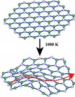
al-lowed. This implies the breakdown of the 2D periodicity in the corresponding lattice. Under these circumstances the long-range periodicity is destroyed by the rippling of the 2D lattice. In compliance with these arguments one expects that a finite-size flake of diameter Dⱗ10a1 can be stable since phonon modes with long wavelengths are not allowed. We carried out ab initio molecular-dynamics 共MD兲 calculations at T = 1000 K on hexagonal finite-size BN flakes with time steps␦t = 2⫻10−15 s. As shown in Fig.4, the structure of the flake was rippled but was not destroyed after 200 time steps.
V. 1D BN NANORIBBONS
Similar to graphene,45 two unique orientations in the 2D BN yield nanoribbons with uniform edges. These are ABNNR and ZBNNR nanoribbons. The profile of the atomic configuration at both edges of the nanoribbon determines their electronic and magnetic properties. The properties can be modified by the passivation of the dangling bond of edge atoms by hydrogen. Because of their interesting electronic and spintronic properties, BN nanoribbons are attractive nanostructures for various device applications. Electronic properties of BN nanoribbons have been investigated in re-cent papers.16–18The present study is complementary to pre-vious studies.
A. Electronic structure
Here we present the results of our study on the electronic and magnetic properties of bare and hydrogen-passivated ABNNR and ZBNNRs. Bare and hydrogen passivation ABNNR are wide band-gap semiconductors. Similarly, hydrogen-passivated ZBNNRs are also semiconductor. The band gaps of these BN nanoribbons depend on the width of
FIG. 3. 共Color online兲 Calculated phonon frequencies versus k vectors. 共a兲 h-BN crystal. 共b兲 1D BN atomic chain. 共c兲 2D BN honeycomb structure. Phonon modes calculated by force-constant direct method are shown by the green-dashed curve.共d兲 Density of phonon frequencies共DOS兲 for the 2D BN honeycomb structure.
FIG. 4. 共Color online兲 Upper: ideal structure of a hexagonal BN flake. Lower: atomic structure of the same flake after 200 time steps of first-principles MD calculations carried out at 1000 K. The rip-pling of 2D structure is shown by the dashed arrow.
the nanoribbons w or the numbers of BN pairs, n, in the primitive unit cell. The variation in the band gap EG as a
function of n is given in Fig. 5. Normally, the properties of nanoribbons approaches those of the 2D honeycomb struc-ture as the width n→⬁. However, due to the localized edge states the band gap of ZBNNR approaches a gap smaller than that of the 2D BN honeycomb structure.17 For narrow 共n⬍8兲 bare and hydrogen-passivated ABNNRs the band gaps vary with n, but they are practically unaltered for n ⬎8. For n⬎8 the band gap of bare ABNNR is 0.4 eV smaller than that of hydrogen-passivated ABNNR. The band gap of hydrogen-passivated ZBNNR is 4.5 eV for n = 3 but decrease to 3.8 eV for n = 16. However, its variation with n is not monotonic for 5⬍n⬍13; it rather displays family-dependent oscillatory variation with changes as large as 0.4 eV between two consecutive values of n. On the other hand, bare ZBNNRs are found to be metallic.
The atomic and electronic structures of bare and hydrogen-passivated ABNNR are described in Fig. 6 for n = 12. The atoms at the edges of the bare ABNNR are recon-structed; while all boron atoms at the edge are lowered and adjacent nitrogen atoms are raised. The reconstruction pat-tern was not affected when the structure optimization is car-ried using double unit cells. Two bands of edge states occur just below the conduction band edge. These two bands are normally degenerate when n is large, but the degeneracy is split when two edges start to couple. Filled bands of edge states occur ⬃−1 eV below the top of the valance band edge. Normal states, on the other hand, have charge distrib-uted uniformly in the ribbon. Because of the edge states the band gap is indirect and is⬃4.22 eV wide. As reported earlier,17 band gaps of hydrogen-passivated ABNNRs converge to a value that is 0.02 eV smaller than the band gap of 2D BN sheet. This difference is relatively higher 共⬇0.1 eV兲 in our results. Furthermore our calculations re-veal such a behavior for bare armchair nanoribbons. The band-gap value of bare nanoribbons converges to a value that is⬇0.4 eV smaller than the 2D band gap. Upon passivation
of the dangling bonds of B and N atoms situated at the edges with hydrogen atoms, these edge state bands are discarded from the band gap and reconstruction of edge atoms disap-pear. At the end, the band gap of H-passivated ABNNR be-comes direct and increases by⬃0.3 eV.
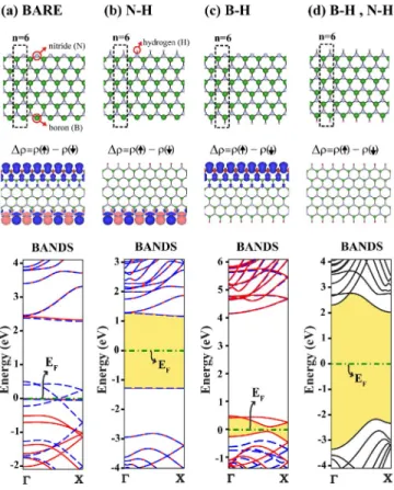
The electronic and magnetic states of ZBNNR depend on whether their edges are passivated with hydrogen atoms. While a bare ZBNNR is magnetic and metallic, it becomes nonmagnetic and a wide band-gap semiconductor upon the passivation of B and N atoms at both edges. Moreover, its electronic and magnetic properties depend on whether only B or N side is passivated with hydrogen atoms. Accordingly, ZBNNRs provide us several alternatives for different elec-tronic and magnetic properties.18 However, different mag-netic states corresponding to different edge configuration, namely, bare or hydrogen passivated, are very sensitive to the parameters of the calculation. In Fig. 7 we present the calculated electronic structures of a ZBNNR with n = 6 B-N pairs in a primitive unit cell for four different cases. These are both side free, only N-side is passivated with hydrogen, only B-side is passivated with hydrogen, and both edges are passivated with hydrogen.
Bare ZBNNR having both edges that are free display dif-ferent magnetic states 共magnetic order兲, which are close in energy. Moreover, the ordering of these magnetic states with respect to their energy is sensitive to the criterion of energy convergence. To ensure the antiferromagnetic 共AFM兲 order at edges, we considered double cells. The possible magnetic states are spin up, spin down for adjacent B atoms at one side and spin up, spin up for the adjacent N atoms at the other
FIG. 5. 共Color online兲 Energy band gap versus the width of the nanoribbons given in terms of the number of B-N atom pairs in the primitive unit cell, n. Bare armchair nanoribbons ABNNR, hydrogen-passivated ABNNR, and hydrogen-passivated zigzag na-noribbons ZBNNR. Dotted line indicates the bulk band gap of 2D BN.
FIG. 6. 共Color online兲 共a兲 Energy-band structure of bare arm-chair nanoribbon ABNNR having n = 12 B-N pairs in the primitive unit cell. At the right-hand side of the bands, the schematic descrip-tion of atomic structure with primitive unit cell delineated by dotted lines and isosurface charge distribution of specific states are shown. 共b兲 Same as 共a兲 but the dangling bonds at both edges are passivated by hydrogen atoms.
side, namely,↑↓ / ↑↑ spin configuration. Other possible spin configurations are↑↑ / ↓↓, ↑↑ / ↑↑, ↑↑ / ↑↓, and ↑↓ / ↑↑. We found that the spin configuration,↑↓ / ↑↑ for ZBNNR having 12 B-N pairs in a double unit cell, corresponds to the ground state. The other excited configurations, ↑↑ / ↓↓, ↑↑ / ↑↑,
↑↑ / ↑↓, and ↑↓ / ↑↓, have 6, 7, 35, and 131 meV higher total
energies than the ground state. The orderings of these con-figurations are slightly different from that reported earlier.18 Although the reported ground-state configuration is the same as ours, excited-state orderings are different. For example, the ↑↓ / ↑↓ state is the lowest energetic excited state in our case, while it is reported as the most energetic excited state in Barone and Peralta.18This might be related with the meth-ods used. Nevertheless, the difference between the earlier and present ground-state energies are within the accuracy limits of the DFT calculations. The ground-state spin con-figuration↑↓ / ↑↑ of the bare ZBNNR having both edges free is found to be a ferrimagnetic metal with = 1.77B per
double cell, whereas the excited magnetic state with configu-ration ↑↑ / ↓↓ is half metallic. Using the calculated energy difference between AFM and FM states we obtain a rough
estimate of the Curie temperature of ZBNNR as TC
⯝379 K for n=6.
In Fig.7共b兲, ZBNNR with N edge passivated with hydro-gen atoms is an AFM semiconductor. The AFM edge state is localized at the B side. When only the B side is passivated with hydrogen atoms the magnetic edge state is, this time, localized at the N side of the ribbon. As seen in Fig.7共c兲the ground state of ZBNNR is ferromagnetic with = 2B per
double cell. Our calculations suggest that the nearest-neighbor N-N interaction is ferromagnetic and the B-B inter-action is antiferromagnetic. Finally, the ZBNNR becomes nonmagnetic when the atoms at both edges are passivated with hydrogen atoms. Earlier, Park and Louie17 studied hydrogen-passivated ABNNRs and ZBNNRs with widths of up to 10 nm. Our results for hydrogen-passivated nanorib-bons are in good agreement with their results, except that our results for zigzag ribbons obtained using GGA as well as LDA exhibit family-dependent oscillations for 5⬍n⬍13.
B. Elastic properties
The elastic properties of BNNRs are examined through the variation in the total energy ETwith respect to the applied
uniaxial strain ⑀=⌬c/c, with c being the lattice constant along the nanoribbon axis. Owing to ambiguities in defining the cross section of the ribbon one cannot determine Young’s modulus rigorously. Instead we calculate =2E
T/c2 from
the variation in ET to specify the elastic properties of
quasi-1D nanoribbons. In Fig.8共a兲we show the variation in the total energy ET versus ⑀. In order to lift the constraints
imposed by periodic boundary conditions, calculations are performed for a supercell comprising five primitive unit cells having lattice constant cs= 5c. For ⑀⬍0.10, the variation in
ET共⑀兲 is parabolic, and hence is independent of ⑀. For⑀
⬎10 the ET共⑀兲 curve deviates from parabola and becomes
anharmonic. For higher values of strain in the plastic region, the ribbon undergoes structural transformation. For example, such a transformation occurred at ⑀= 0.24 with a sudden change in the ET共⑀兲 curve. The corresponding structure is
illustrated as inset. The lattice constant csincreased from the
initial value 21.5 Å to 27.4 Å corresponding to ⑀= 0.27. In Fig. 8共b兲 versus the width of the ribbon in terms of the number of B-N pair in the primitive unit cell n is plotted for bare and hydrogen-passivated ABNNR. 共n兲 shows an approximately linear variation, indicating that the force con-stant is directly proportional to the width of the ribbon. One also sees that the strength of the ribbon increases upon pas-sivation with hydrogen.
The behavior of bare and hydrogen-passivated ZBNNR under uniaxial tensile stress is similar to that of ABNNR. In Fig. 9 three regions, namely, elastic harmonic, elastic-anharmonic, and plastic regions are seen. The sudden change in the ET共⑀兲 curve at ⑀⬃0.23 indicates a structural phase
transformation, where the lattice constant cselongates from
the initial ⑀= 0 value of 19.8 to 25.7 Å corresponding to⑀ = 0.3. The structure of hydrogen-passivated ZBNNR before and after the structural transformation is shown as inset. Variation inversus the ribbon width n is calculated for bare and hydrogen-passivated ZBNNR shows an overall linear behavior as presented in Fig. 8共b兲.
FIG. 7.共Color online兲 Top panels: atomic structures of ZBNNR. The primitive unit cell has n = 6 B-N pairs delineated by dotted lines in the top panels. The unit cell is doubled due to the antiferromag-netic interaction between adjacent N atoms. Middle panels: isosur-face plots of difference charge density between up-spin and down-spin states, ⌬=共↑兲−共↓兲. Bottom panels: energy-band structure with dotted 共blue兲 and solid 共red兲 lines showing up and spin-down states, respectively. 共a兲 Bare ZBNNR; 共b兲 B-side free, but N-side is passivated by hydrogen atoms;共c兲 N-side free, but B-side is saturated by hydrogen atoms; 共d兲 both sides are saturated by hydrogen atoms. The bands in 共a兲–共c兲 are calculated using double cell.
C. Vacancy and antisite defects
It is known that the vacancy defect in 2D graphene46–50 and graphene nanoribbons51,52 gives rise to crucial changes in the electronic and magnetic structures. According to Lieb’s theorem,53the net magnetic moment per cell is deter-mined with the difference in the number of atoms belonging to different sublattices, i.e.,=共NB− NN兲B. While DFT cal-culations on vacancies in 2D graphene and armchair graphene nanoribbons confirmed Lieb’s theorem, results are diversified for vacancies in zigzag graphene nanoribbons.51,52 Therefore, the effect of vacancy defects on the properties of BNNRs is of interest.
Earlier activation energies and reaction paths for diffusion and nucleation monovacancy and divacancy in h-BN layers have been investigated by using density-functional tight-binding method. The formation energies were calculated to be 11.22 and 8.91 eV, for B and N vacancies, respectively.54 The possible magnetism induced by nonmagnetic impurities and vacancy defects in a BN sheet has been investigated
from the first principles. The magnetic moment associated by nonmagnetic atoms substituting B or N has been calculated to be 1B.55Based on first-principles calculations, the
mag-netic moment of a N vacancy in a 2D BN sheet has been predicted to be 1B. In the case of a B vacancy, three
neigh-boring N atoms are displaced further apart from each other and the net magnetic moment is predicted to be 3B.56
An-other calculation of defects in a BN monolayer found that three dangling bonds associated with a B vacancy lead to total spin S = 3/2, i.e., 3B.57
The effects of vacancies of BN nanoribbons have not been treated yet. Here we investigate the effect of B, N, B + N divacancy, and B + N antisite on the electronic and magnetic properties of ABNNR and ZBNNR. Within periodic bound-ary conditions, a vacancy defect in an ABNNR of width n = 12 is repeated in every fifth primitive unit cell to yield minute defect-defect coupling. As shown in Fig. 10共a兲 ABNNR with B vacancy becomes ferromagnetic with a net magnetic moment of = 1B per unit cell. Similarly, a N
vacancy gives rise to a net magnetic moment of= 1Bper
unit cell. ABNNRs having either periodic B + N divacancy or antisite defect for every five unit cell remain nonmagnetic. The calculated values of magnetic moments are in compli-ance with Lieb’s theorem. We found that the structural relax-ation is crucial to obtain correct values of magnetic mo-ments. In particular, initially we calculated = 3B for the
relaxed structure of the B vacancy. However, the neighboring N atoms distorted slightly from their equilibrium, the struc-ture is relaxed further and had lowered the total energy. As a result, the magnetic moment was calculated as = 1B. The
energy-band structures in Figs.10共a兲–10共d兲are calculated for periodic vacancy defects repeating in every four primitive cell. The Fermi levels are assigned according to the occu-pancy of vacancy states. We note that the empty state asso-ciated with the B vacancy in Fig. 10is holelike. The states associated with the N vacancy that occur near the edge of the conduction band are donorlike.
The situation with ZBNNR is similar to that in ABNNR discussed above since hydrogen-passivated ZBNNR is
non-FIG. 8. 共Color online兲 共a兲 Variation in the total energy of hydrogen-saturated ABNNR with strain⑀ is shown by the dashed curve with large black dots indicating the calculated data points 共cs= 5c and n = 9兲. Harmonic, anharmonic, and plastic regions are
distinguished. The harmonic part is fitted to a parabola presented by red-solid curve. Atomic structure shown by filled, empty, and very small empty circles represent B, N, and H atoms. Supercell com-prising five primitive unit cells are shown in the harmonic and plastic regions.共b兲 Variation in=2E
T/c2versus the ribbon width
n calculated for bare and hydrogen-passivated ABNNR.
FIG. 9.共Color online兲 Variation in the total energy of hydrogen-saturated ZBNNR shown by the dashed curve with large black dots indicating the calculated data points. Harmonic, anharmonic, and plastic regions are distinguished. The harmonic part is fitted to a parabola presented by a red-solid curve. Atomic structure of the ribbon in a supercell comprising eight unit cells共cs= 8c and n = 6兲
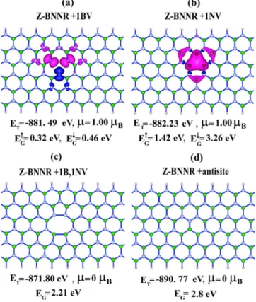
magnetic as ABNNR. As shown in Fig.11, a periodic B or N vacancy repeated in every eight unit cell of hydrogen-saturated ZBNNR with n = 6 has a net magnetic moment of
= 1Bper supercell. ZBNNR passivated with hydrogen
at-oms at both edges and having either periodic B + N diva-cancy or antisite defect repeating in every eight unit cell is nonmagnetic. The type of the periodic vacancy defect modi-fies the band gap of ZBNNR from 4.2 to 2.21 eV for diva-cancy but to 2.8 eV for antisite. The calculated magnetic moment of hydrogen-passivated ZBNNR is in agreement with Lieb’s theorem. We note that in zigzag graphene nanor-ibbons magnetic edge states survive even after hydrogen pas-sivation and interact with the magnetic moments of vacancies.52 This interaction causes deviation from the pre-diction of Lieb’s theorem.
VI. DISCUSSION AND CONCLUSIONS
In various allotropic forms of BN the dimensionality play a crucial role. For the sake of comparison, we present the calculated values of BN for different allotropic forms of BN in different dimensionalities. One sees that the B-N double bond of 1D BN atomic chain is shortest and is 1.31 Å. The sp2 bond of h-BN and 2D BN has an intermediate value of 1.45 Å. Therefore, h-BN can be considered as quasi-two-dimensional. Three-dimensional wurtzite and zinc-blende BN crystal have sp3bonding with d = 1.56 Å, which is larg-est among the allotropic forms studied here. According to
GGA results the cohesive energy of 2D BN is 3 meV larger than that of h-BN. This is due to the fact that the GGA calculation cannot account the van der Waals interaction be-tween atomic layers of h-BN. However, the calculations us-ing LDA, where the van der Waals interactions are better accounted, yield the cohesive energy of h-BN which is ⬃57 meV larger than that of the 2D BN as one expects. The charge transfer⌬Q from B to N atom increases with decreas-ing dimensionality. This is due to fact that d decreases with decreasing dimensionality. The coordination number in-creases with increasing dimension.
In 2D BN honeycomb structures and in its zigzag and armchair nanoribbons, the B-N bond formed from the bond-ing sp2 hybrid orbitals from B and N atoms is essential. Owing to the transfer of charge from B to N the B-N bond acquires an ionic character, which underlies the semicon-ducting properties with wide band gap.
Bare armchair nanoribbon of 2D BN is again a nonmag-netic wide band-gap semiconductor, the band gap of which is practically unaltered with width n⬎8. Upon passivation with hydrogen, band gap of the ribbon increases by 0.3 eV. As for zigzag nanoribbons, they provide a number of interesting properties. When its both edges are bare, it is ferromagnetic metal. When its N edge is passivated with hydrogen, it be-comes an antiferromagnetic semiconductor. In the reverse case, namely, when the B side is passivated, it becomes a
FIG. 10. 共Color online兲 Relaxed atomic structures and corre-sponding energy bands of hydrogen-passivated ABNNR with n = 12 having a point defect located periodically in every four primi-tive cell. Blue filled, empty, and small circles represent B, N, and H atoms, respectively. Pink/light and blue/dark isosurface plots are for spin-up and spin-down states. 共a兲 Single B vacancy; 共b兲 single N vacancy;共c兲 B-N divacancy; 共d兲 antisite defect.
FIG. 11. 共Color online兲 Relaxed atomic structures of hydrogen-passivated ZBNNR with n = 6 having a vacancy defect located pe-riodically in every eight primitive cell 共cs⬇8c and n=6兲. Filled,
empty, and small circles represent B, N, and H atoms, respectively. Pink and blue isosurface plots are spin-up and spin-down states, respectively. 共a兲 Single B vacancy; 共b兲 single N vacancy; 共c兲 B + N divacancy;共d兲 antisite defect.
ferromagnetic semiconductor. When both edges are passi-vated, it becomes a nonmagnetic wide band-gap semicon-ductor. The band gap as well as the magnetic state of a rib-bon can be modified by periodic vacancy defects. Finally, BN nanoribbons have been found to be strong, quasi-one-dimensional, and stable structures. They can sustain up to high strains, and they stretch in the plastic region with struc-tural transformations.
Briefly, the calculated electronic, magnetic, and mechani-cal properties of 2D BN honeycomb structure and its nanor-ibbons present interesting but some differences from graphene. In this respect BN honeycomb structure and its nanoribbons are complimentary to graphene. The properties
of 2D BN honeycomb structure can be changed upon func-tionalization with foreign atoms. Interesting quantum struc-tures 共such as single and series quantum dots, resonant tun-neling double barriers, and multiple quantum well structures兲 based on heterostructures and core shell structures of lattice matched graphene and BN can be formed, since the band gap of BN is much larger than that of graphene.
ACKNOWLEDGMENTS
Part of the computational resources has been provided by UYBHM at Istanbul Technical University through Grant No. 2-024-2007.
1K. S. Novoselov, A. K. Geim, S. V. Morozov, D. Jiang, Y.
Zhang, S. V. Dubonos, I. V. Grigorieva, and A. A. Firsov, Sci-ence 306, 666共2004兲.
2Y. Zhang, Y.-W. Tan, H. L. Stormer, and P. Kim, Nature
共Lon-don兲 438, 201 共2005兲.
3C. Berger, Z. Song, X. Li, X. Wu, N. Brown, C. Naud, D.
Mayou, T. Li, J. Hass, A. N. Marchenkov, E. H. Conrad, P. N. First, and W. A. de Heer, Science 312, 1191共2006兲.
4A. K. Geim and K. S. Novoselov, Nature Mater. 6, 183共2007兲. 5Y.-W. Son, M. L. Cohen, and S. G. Louie, Nature共London兲 444,
347共2006兲.
6H. Sevinçli, M. Topsakal, E. Durgun, and S. Ciraci, Phys. Rev. B
77, 195434共2008兲.
7M. Topsakal, H. Sevinçli, and S. Ciraci, Appl. Phys. Lett. 92,
173118共2008兲.
8K. S. Novoselov, D. Jiang, F. Schedin, T. Booth, V. V.
Khot-kevich, S. Morozov, and A. K. Geim, Proc. Natl. Acad. Sci. U.S.A. 102, 10451共2005兲.
9D. Pacilé, J. C. Meyer, Ç. Ö. Girit, and A. Zettl, Appl. Phys.
Lett. 92, 133107共2008兲.
10A. Nagashima, N. Tejima, Y. Gamou, T. Kawai, and C. Oshima,
Phys. Rev. Lett. 75, 3918共1995兲.
11L. Bourgeois, Y. Bando, W. Q. Han, and T. Sato, Phys. Rev. B
61, 7686共2000兲.
12N. G. Chopra, R. J. Luyken, K. Cherrey, V. H. Crespi, M. L.
Cohen, S. G. Louie, and A. Zettl, Science 269, 966共1995兲.
13C. Zhi, Y. Bando, C. Tang, and D. Golberg, Appl. Phys. Lett. 87,
063107共2005兲.
14D. Golberg, A. Rode, Y. Bando, M. Mitome, E. Gamaly, and B.
Luther-Davies, Diamond Relat. Mater. 12, 1269共2003兲.
15Y. J. Chen, H. Z. Zhang, and Y. Chen, Nanotechnology 17, 786
共2006兲.
16Z. Zhang and W. Guo, Phys. Rev. B 77, 075403共2008兲. 17Cheol-Hwan Park and Steven G. Louie, Nano Lett. 8, 2200
共2008兲.
18V. Barone and J. E. Peralta, Nano Lett. 8, 2210共2008兲. 19X. Li, L. Zhang, S. Lee, and H. Dai, Science 319, 1229共2008兲. 20X. Wang, Y. Ouyang, X. Li, H. Wang, J. Guo, and H. Dai, Phys.
Rev. Lett. 100, 206803共2008兲.
21P. E. Blöchl, Phys. Rev. B 50, 17953共1994兲.
22J. P. Perdew, J. A. Chevary, S. H. Vosko, K. A. Jackson, M. R.
Pederson, D. J. Singh, and C. Fiolhais, Phys. Rev. B 46, 6671 共1992兲.
23G. Kresse and J. Hafner, Phys. Rev. B 47, 558共1993兲. 24G. Kresse and J. Furthmüller, Phys. Rev. B 54, 11169共1996兲. 25S. Baroni, A. Del Corso, S. Girancoli, and P. Giannozzi, http:/
www.pwscf.org/
26A. Catellani, M. Posternak, A. Baldereschi, and A. J. Freeman,
Phys. Rev. B 36, 6105共1987兲.
27L. Liu, Y. P. Feng, and Z. X. Shen, Phys. Rev. B 68, 104102
共2003兲.
28N. Ooi, V. Rajan, J. Gottlieb, Y. Catherine, and J. B. Adams,
Modell. Simul. Mater. Sci. Eng. 14, 515共2006兲.
29K. Shimada, T. Sota, and K. Suzuki, J. Appl. Phys. 84, 4951
共1998兲.
30M. P. Surh, S. G. Louie, and M. L. Cohen, Phys. Rev. B 43,
9126共1991兲.
31R. T. Senger, S. Tongay, E. Durgun, and S. Ciraci, Phys. Rev. B
72, 075419共2005兲.
32A. V. Kurdyumov, V. L. Solozhenko, and W. B. Zelyavski, J.
Appl. Crystallogr. 28, 540共1995兲.
33Caution has to be taken in using the values of band gap
calcu-lated with DFT as in the present study, since the value of band gap is usually underestimated by DFT.
34The calculations of⌬Q have been carried out by using thePWSCF
software共Ref.25兲. It should be noted that the ground-state prop-erties do not differ no matter when lattice constants and atomic configurations are optimized using eitherVASPorPWSCF. 35S. Tongay, R. T. Senger, S. Dag, and S. Ciraci, Phys. Rev. Lett.
93, 136404共2004兲.
36E. Rokuta, Y. Hasegawa, K. Suzuki, Y. Gamou, C. Oshima, and
A. Nagashima, Phys. Rev. Lett. 79, 4609共1997兲.
37L. Wirtz, A. Rubio, R. A. delaConcha, and A. Loiseau, Phys.
Rev. B 68, 045425共2003兲.
38G. Kern, G. Kresse, and J. Hafner, Phys. Rev. B 59, 8551
共1999兲.
39W. J. Yu, W. M. Lau, S. P. Chan, Z. F. Liu, and Q. Q. Zheng,
Phys. Rev. B 67, 014108共2003兲.
40J. Serrano, A. Bosak, R. Arenal, M. Krisch, K. Watanabe, T.
Taniguchi, H. Kanda, A. Rubio, and L. Wirtz, Phys. Rev. Lett. 98, 095503共2007兲.
41V. L. Solozhenko, G. Will, and F. Elf, Solid State Commun. 96,
42Y. Miyamoto, M. L. Cohen, and S. G. Louie, Phys. Rev. B 52,
14971共1995兲.
43F. Liu, P. Ming, and J. Li, Phys. Rev. B 76, 064120共2007兲. 44D. Alfè, http://chianti.geol.ucl.ac.uk/dario
45V. Barone, O. Hod, and G. E. Scuseria, Nano Lett. 6, 2748
共2006兲.
46P. Esquinazi, D. Spemann, R. Höhne, A. Setzer, K.-H. Han, and
T. Butz, Phys. Rev. Lett. 91, 227201共2003兲.
47A. Hashimoto, K. Suenaga, A. Gloter, K. Urita, and S. Iijima,
Nature共London兲 430, 870 共2004兲.
48O. V. Yazyev and L. Helm, Phys. Rev. B 75, 125408共2007兲. 49M. A. H. Vozmediano, M. P. Lopez-Sancho, T. Stauber, and F.
Guinea, Phys. Rev. B 72, 155121共2005兲.
50L. Brey, H. A. Fertig, and S. Das Sarma, Phys. Rev. Lett. 99,
116802共2007兲.
51J. J. Palacios, J. Fernandez-Rossier, and L. Brey, Phys. Rev. B
77, 195428共2008兲.
52M. Topsakal, E. Aktürk, H. Sevinçli, and S. Ciraci, Phys. Rev. B
78, 235435共2008兲.
53E. H. Lieb, Phys. Rev. Lett. 62, 1201共1989兲.
54A. Zobelli, C. P. Ewels, A. Gloter, and G. Seifert, Phys. Rev. B
75, 094104共2007兲.
55R. F. Liu and C. Cheng, Phys. Rev. B 76, 014405共2007兲. 56M. S. Si and D. S. Xue, Phys. Rev. B 75, 193409共2007兲. 57S. Azevedo, J. R. Kashny, C. M. C. de Castilho, and F. De Brito,