♠Corresponding author, e-mail: [email protected]
The Effect of Growth Conditions on The Optical and
Structural Properties of InGaN/GaN MQW LED
Structures Grown by MOCVD
S.Ş. ÇETĐN
1,2,♠, S. SAĞLAM
1,2, S. ÖZÇELĐK
1,2, E. ÖZBAY
31
Department of Physics, Faculty of Sciences, Gazi University, 06500, Teknikokullar, Ankara, TURKEY
2
Photonics Application and Research Center, Gazi University, 06500, Teknikokullar, Ankara, TURKEY
3
Nanotechnology Research Center, Department of Physics, Department of Electrical and Electronics Engineering, Bilkent University, 06800, Bilkent Ankara, TURKEY
Received: 27/08/2014 Accepted:14/10/2014
ABSTRACT
Five period InGaN/GaN MQW LED wafers were grown by low pressure MOCVD on an AlN buffer layer, which was deposited on a c-plane (0001)-faced sapphire substrate. The effect of growth conditions, such as the well growth time, growth temperatures, and indium flow rate on the properties of MQW structures were investigated by using high resolution X-ray diffraction and room temperature photoluminescence. By increasing growth temperature, the emission wavelengths showed a blue-shift while it red-shifted via an increase in the indium flow rate. The emission wavelength can be tuned by way of changing the well growth time of the samples.
Keywords: Metalorganic chemical vapor deposition; InGaN, Light emitting diode; Multi quantum well; High resolution X-ray diffraction; Photoluminescence
1. INTRODUCTION
InGaN/GaN multi quantum well (MQW) structures are used extensively as the active layer in blue, green, and yellow light emitting diode applications [1-9]. It is well known that the structural and optical characteristics of InGaN/GaN MQWs are quite sensitive to the growth conditions of the active layer such as the flow rate of the species of the alloy, growth pressure, well/barrier growth time, and growth temperature. The slight adjustment of these conditions, especially of growth time and growth temperature, could improve the quality of the MQWs. Additionally, tuning of the emission wavelengths of the LED structures can be possible by these adjustments. For the fabrication of optoelectronic devices, InGaN material has been used as the active material for several years. Despite the wide use of this material, in growing
high quality InGaN layer there are still some problems such as composition inhomogeneity or fluctuation and indium droplets, indium surface segration etc. Also, the emission properties and structural quality of the active layers in the nitride alloys have been affected by piezoelectric effect, strain relaxation. Many research groups aimed to reduce these problems and have been studying for improving the quality of this type of MQW structures by using different growth conditions, such as selecting the nucleation layer, well/barrier growth time, growth temperature of the layers etc. [10-17]. However, the effect of the well layer growth time on emission and structural properties is not widely studied. In addition to these, the selection of a buffer layer is quite important to improve the crystal quality. Recently, thick SI-GaN layers grown on an HT-AlN buffer layer/sapphire substrate by metalorganic chemical vapor deposition (MOCVD) has been shown to have highly improved quality [11-13].
In the present study, five period InGaN/GaN MQWs were grown on a high temperature AlN buffer layer on a sapphire substrate by using MOCVD under different growth conditions in order to improve the quality of InGaN/GaN MQWs for blue LED applications. For the optimization of the optical properties of LED applications, the effect of the well growth time, growth temperature, and In flow rate on the optical and structural properties of InGaN/GaN MQWs were investigated by using high resolution X-ray diffraction (HRXRD) and room temperature photoluminescence (RT-PL). Also, transmittance measurement of InGaN/GaN samples was determined by UV-VIS spectroscopy at the room temperature.
2. EXPERIMENTAL
The six LED structures containing five period InGaN/GaN multi quantum well (MQW) were grown by MOCVD on c-plane (0001)-faced sapphire substrates with a 10 nm low-temperature AlN nucleation layer. The AlN nucleation and the AlN buffer layer were grown on the sapphire substrate with the aim of the reducing the lattice mismatch. Hydrogen was used as the carrier gas, in which trimethylgallium (TMGa), trimethylaluminum (TMAl), trimethylindium (TMIn) and ammonia (NH3) were used as source compounds. During the growth, the reactor pressure
was kept at 200 mbar. A 10nm-thick AlN nucleation layer was deposited at 840 °C, and then the reactor temperature was ramped to 1150 °C and a 400 nm AlN buffer layer was grown, followed by a 2-min growth interruption in order to reach the optimal growth conditions for GaN. A 340 nm GaN buffer layer was grown at 1080 °C. A thick n-type GaN:Si layer with a thickness of 1600 nm was grown on the GaN buffer layer for all of the samples. Quantum well layers were formed in a manner that each 2 nm InxGa1-xN active layer was separated from one another by a thin 9 nm GaN that was grown in different conditions. Finally, a 160 nm thick p-type GaN:Mg cap layer was deposited on the MQWs at 1030 °C [21].
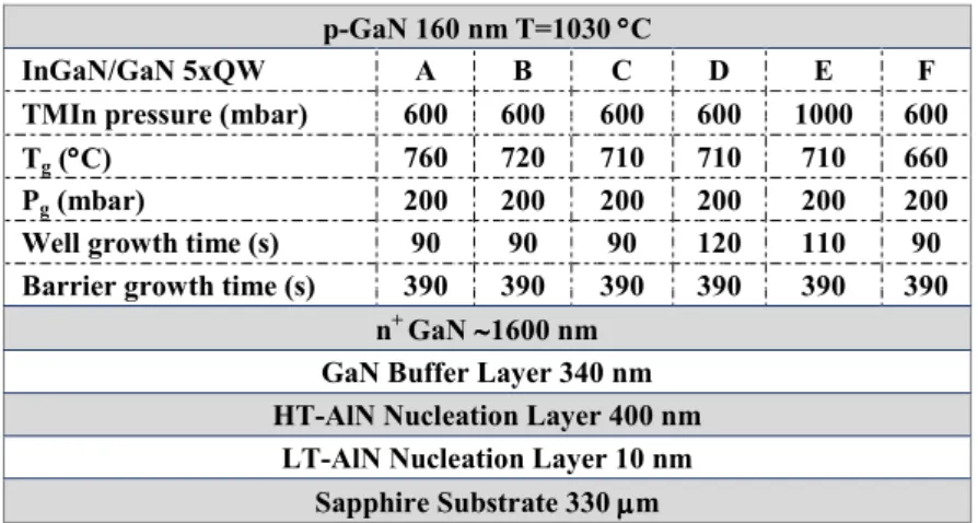
Samples named A, B, C, and F were grown at the same well growth time (90 s) and at different growth temperatures, 760 °C, 720 °C, 710 °C, and 660 °C, respectively. The other sample, named D, was grown by well growth time of 120 s at 710 °C. During the growth of sample E, TMIn pressure was kept at 1000 mbar while the others were grown under the TMIn pressure of 600 mbar. Moreover, the well growth time for sample E was 110 s. All of the grown structures with different growth conditions are shown in Fig. 1.
p-GaN 160 nm T=1030 °°°°C
InGaN/GaN 5xQW A B C D E F
TMIn pressure (mbar) 600 600 600 600 1000 600
Tg (°°°°C) 760 720 710 710 710 660
Pg (mbar) 200 200 200 200 200 200
Well growth time (s) 90 90 90 120 110 90
Barrier growth time (s) 390 390 390 390 390 390 n+ GaN ∼∼∼∼1600 nm
GaN Buffer Layer 340 nm HT-AlN Nucleation Layer 400 nm
LT-AlN Nucleation Layer 10 nm Sapphire Substrate 330 µµµm µ
Fig. 1. Six of the five period InGaN/GaN MQW structures (A, B, C, D, E, and F) that were grown under various growth temperatures, barrier growth times, and In flow rate.
High resolution X-ray diffraction (HRXRD) is a very useful technique to determine lattice constants, alloy compositions and crystalline quality for nitride based semiconductor alloys. The fundamental optical band edge transition and impurity related transitions of semiconductors can be measured by using photoluminescence (PL) spectroscopy [18, 19]. Also, the analysis of optical absorption spectra is one of the most productive tools for understanding and developing the band structure and energy gap of materials [20]. X-ray measurements were carried out on a D-8 Bruker high-resolution diffractometer by using CuKα1 (1.540 Å) radiation, a prodded mirror, and a 4-bounce Ge (220) symmetric monochromator. With the Si calibration sample, its best resolution was 16 arcsec. Room temperature PL measurements were performed by using the Jobin Yuvon Florog-550 system with a 50 mW He-Cd laser (λ=325 nm) as an excitation light source. The transmittance
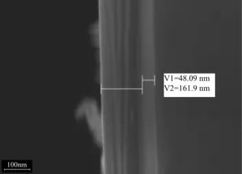
measurements were examined with a Perkin Elmer 45 UV-VIS-near-infrared spectrometer, in the wavelength range from 200 to 1100 nm. In addition, the total QW thickness of sample C was obtained by using a high resolution scanning electron microscope (SEM).
3. RESULTS AND DISCUSSION
HRXRD measurements were used to evaluate the quality of the QWs and the interfaces, determine thickness of the layers and the In composition in the wells. ω-2θ scans for the (0002) reflection from five-period InGaN/GaN MQW LED structures A, B, C, D, E, and F grown at different well growth times and growth temperatures were obtained by using the HRXRD system. The HRXRD profile of the B, C, and E samples is shown in Fig. 2, respectively, as an example. The strongest peaks were from the diffraction of
the thick GaN layer over the buffer layer, while the second strongest peaks with an angle of 18° were from the AlN buffer layer. The satellite peaks originated from the diffraction of the InGaN/GaN MQWs.
2θθθ-axis (degree)θ 16.0 16.5 17.0 17.5 18.0 18.5 In te n s it y ( a rb .u .) E C B SL-2 SL-1 SL0 GaN AlN
Fig. 2. The 2θ-axis scan for the (0002) reflection of the 5 period MQW samples.
The average indium composition can be calculated from the angular separation of the 0th satellite peak (SL0) with respect to the main GaN peak. By using the HRXRD data, the estimated In compositions of Ga rich well in the samples A, B, C, D, E, and F are 5.2%, 6.5%, 9.7%, 9.8%, 12.8%, and 12.9%, respectively, by using LEPTOS simulating software [22]. The lower indium composition of samples A and B compared to the others can be explained by the fact that the increase in the volatility of indium along with the higher growth temperature. When the growth temperature increased from 660 °C to 760 °C (samples F and A), the indium mole fraction is also decreased by 40.3 percent. In other words, the average of the indium mole fraction is decreased via the increase of the growth
temperature.
The increasing well growth time from 90 s to 120 s for the samples C and D showed that the indium composition was slightly increased with increasing growth time. For sample E, indium content is bigger than sample D with same Tg although well growth time for sample E is smaller than sample D. At the same time, the sample E was grown at a higher TMIn flow rate than others. These results indicated that TMIn flow rate is dominant on the indium mole fraction.
The full width half maximums (FWHM) of the satellite peaks in turn point out the high interface quality and good well periodicity. It was found that the FWHM values of the satellite peaks were decreased with increasing Tg from 660 °C (for F) to 710 °C (for C), 720 °C (for B) and 760 °C (for A). Therefore, the crystalline quality was improved by decreasing the indium content [23]. Additionally, the FWHM of the XRD first satellite peak value (SL-1) of samples C, D, and E were measured as 336, 353, and 338 arcsec, respectively. The FWHM value of sample C was the lowest. In other words, the crystalline quality was also improved via lower well growth time.
Furthermore, the well thickness of samples A-F were determined by using the HRXRD results as 1.6 nm /8.3 nm, 1.65 nm/8.4 nm, 1.7 nm/8.5 nm, 2.1 nm/9 nm, 2.8 nm/9.2 nm, and 2.9 nm/9.3 nm, respectively. As an example, the total QW and cap layer thicknesses of sample C were obtained as 48.09 nm and 161.9 nm by using a scanning electron microscope (SEM), respectively, as shown in Fig. 3. The total QW and cap layer thicknesses of this sample were determined by using the XRD data 51 nm and 159 nm, respectively. The obtained results via these two tools were in good agreement. This indicated that the obtained thickness values by HRXRD measurements are trusty although the InxGa1-xN peaks are broadened due to compositional fluctuations in these material systems.
Fig. 3. High resolution SEM image of sample C. V1 is the total QW thickness and V2 is the cap layer thickness.
V1=48.09 nm V2=161.9 nm
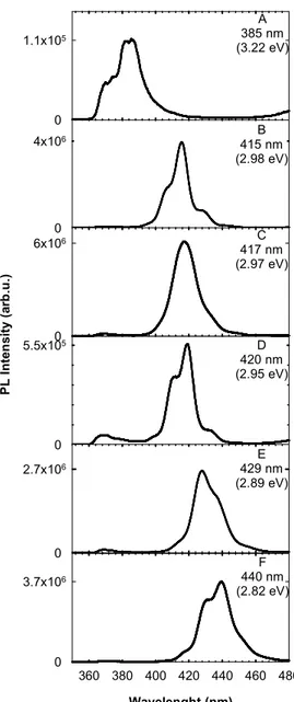
P L I n te n s it y ( a rb .u .) 0 5.5x10⁵ 0 4x10⁶ 0 6x10⁶ 0 2.7x10⁶ Wavelenght (nm) 360 380 400 420 440 460 480 0 3.7x10⁶ 0 1.1x10⁵ B 415 nm (2.98 eV) A 385 nm (3.22 eV) C 417 nm (2.97 eV) D 420 nm (2.95 eV) E 429 nm (2.89 eV) F 440 nm (2.82 eV)
Fig. 4. Room temperature photoluminescence spectra versus photon wavelength of the samples.
The room temperature PL spectra of the MQW samples A-F are shown in A-Fig. 4. The Indium content in InGaN epilayers decreases due to the increase of Tg and decreasing well growth time, which make wavelength tunability possible for this set of epilayers. Some impurity peaks were observed along with band edge peaks for all samples. At low temperature of 660 °C (sample F), these impurity peaks were more dominant than the others. Therefore, the FWHM of the emission peak of the sample F is bigger with respect to the others. As shown in Table 1, FHWM of the bang edge emission peak was increased with increasing indium composition except sample A. The impurity peaks in PL emission of B and C samples were found out to be weaker than the other samples. Also, the PL intensity increases and their FWHM values decrease at high temperatures. Hence, this shows the improvement in optical quality and is consistent with the XRD rocking curve results. However, in case of sample A which has very low indium content, the emission peak showed different behavior compared to the
other samples. The broadening in the PL peak of the sample A can be explained by the dominant inhomogenity of indium content in the well layer. Also, the emission of the InGaN could not separate from GaN emission because of the rich Ga content in this layer of the sample.
Also we concluded that the effects of growth conditions on the tuning of wavelength are as following: Although samples A, B, C, D, and F were nearly grown under the same TMIn flow condition (600 mbar), the room temperature PL emission wavelength peak of sample B that was grown at 720 °C blue-shifted compared to samples C, D and F, which were grown at 710 °C as shown in Fig. 4. This indicates that the decrease in indium incorporation and the emission wavelength of the QW is blue-shifted. In spite of that, the growth temperature of sample E was the same as samples C and D, in which the average of the indium mole fraction for sample E was increased by the higher TMIn flow rate to where the peak emission wavelength showed a ∆λ=12 nm red-shift for sample C. As a result, the growth temperature and TMIn flow rate have a main role in indium incorporation during the growth of InGaN/GaN MQWs. However, despite the growth temperature, the TMIn flow rate for samples C and D were the same, in which the RT-PL emission peak of sample D red-shifted compared to sample C as shown in Fig. 4. In other words, the emission wavelength was tuned to approximately ∆λ=3 nm when the well growth time was increased by 30 s. This shifting of the wavelength is small. However, as increasing of Tg caused forming the impurity peaks. It is clear that the red-shift in the emission wavelength of sample D was related to the quantum size effect that came from the strain fluctuations depending on the In composition fluctuation during the growth of MQWs [24]. It is well known that the strain between the well and barrier layers and also increasing of the barrier layer thickness induce a piezoelectric field which leads to the anomalous behavior of the quantum-confined Stark effect [25, 26]. Thus, the lower PL intensity and red-shift of the emission energy of sample D can also be explained by the quantum confined stark effect [25]. On the other hand, the well growth time of samples C, D, and E was 90, 120, and 110 s, respectively. The PL peak intensity of these samples increased while the well growth time was decreased. This can in turn improve crystal quality [14].
The band gaps of the samples were also determined from the absorption edges by optical absorption measurements. The analysis of optical absorption spectra is one of the most productive tools for understanding and developing the band structure and energy gap of materials [20]. If epitaxial layer allows direct transition, the threshold of the fundamental absorption, is given by the expression:
2 0
(α νh ) =α(hν−Eg),
where E=hν is the photon energy, Eg is the optical band gap
and α0 is a constant which does not depend on photon
energy and α is absorption coefficient which can calculated by using the following expression:
0
1 ln(T).
d T
Where, T and T0 are measuring transmittance of the
samples and sapphire substrate, respectively. The thickness of the layers (d) was determined by using HRXRD simulation results.
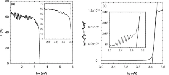
The transmittance spectra of the sample C is presented in Fig. 5(a). The absorption edge located at 3.41 eV which is
corresponds to the energy bandgap of GaN layers. Appearing periodic oscillation below this absorption edge originated from the multi-reflection interference resulting from 1600 nm GaN layer [27]. In the photon energy region of 2.8-3.3 eV, the periodicity of the oscillation was broken and their intensities reduced as seen inset in Fig. 5 (a). The absorptions in this region originated from excitonic transitions in the InGaN well layers.
hν ν ν (eV)ν 2 3 4 5 6 T ( % ) 0 20 40 60 80 (a) 2.8 3.0 3.2 3.4 0 10 20 30 40 50 60 70 hν ν ν ν (eV) 3.0 3.1 3.2 3.3 3.4 3.5 (αααα hνννν )2 (c m -1e V) 2 0 4.0x10⁹ 8.0x10⁹ 1.2x10¹⁰ (b) 2.0 2.4 2.8 3.2 107 2x10⁷ 3x10⁷ 4x10⁷
Fig. 5. (a) Room temperature transmittance spectra of the sample C (the inset represents the transmittance behavior of excitonic transitions region in the InGaN well layers). (b) Room-temperature optical absorption spectra, (αhν)2 versus hν, of GaN layer (the inset is the absorption curve of InGaN layer) for sample C.
Table 1. The band gap energies of all samples.
PL measurement UV-VIS measurement
Sample x (%) Eg (eV) InGaN FWHM (nm) Eg (eV) InGaN Eg (eV) GaN A 5.20 3.22 19 3.17 3.39 B 6.50 2.98 12 3.00 3.41 C 9.75 2.97 17 2.95 3.41 D 9.80 2.95 16 2.97 3.39 E 12.78 2.89 19 2.83 3.38 F 12.90 2.82 20 2.78 3.38
The band gap of the samples determined from the absorption edges using plot (αhν)2 versus hν in the Fig. 5
(b). Extrapolating the linear part of each plot towards lower photon energies, the point of interception with the h
ν
axis exists at (αhν)2=0 giving the corresponding band gap [20].As an example, for GaN and InGaN layers band gap energies in sample C value were determined as 3.41, 2.95 eV, respectively. Obtained this value for InGaN of sample C by UV-VIS measurement is agreement with obtained band gap energy value as 2.97 eV from PL measurement. Obtaining band gap energy values for all of the samples were given in Table 1 as comparison with PL and UV-VIS measurement. As a result, the values of the band gap from both UV-VIS and PL measurements are in good agreement in each other. However, small differences between the band gap energies determined by these two techniques can be
attributed to Stokes shift [28]. 4. CONCLUSIONS
The effect of growth conditions that included the well growth time, growth temperatures, and In flow rate on the optical and structural properties of InGaN/GaN MQW LED structures, which were grown by MOCVD, was investigated. It was determined that the optical and structural qualities of the InGaN/GaN MQW LED structure are strongly depend on these growth parameters. From the XRD measurements we determined the well/barrier thicknesses and indium content of the well layer. The results show that indium incorporation decreased via low indium pressure and a high growth temperature. The room temperature PL peak energy demonstrated a blue-shift with a decreasing indium flow rate and increasing growth
temperature. The obtained results show that the changing of well growth time slightly changed the indium mole fraction ratio of the structures. In result of this, it did create a little shifting of the emission wavelength. Therefore, our results show that the emission wavelength can be tuned by adjusting the well growth time of the samples. In addition, absorption edges were determined by using the transmittance spectra of the samples. Finally, our results also show that quality InGaN/GaN blue LED MQW structures can be grown on sapphire with a high temperature AlN buffer layer by optimizing all the growth conditions, such as the growth temperature, indium pressure, and well growth time.
ACKNOWLEDGEMENTS
This work was supported by DPT under project No. 2011K120290 and by BAP at Gazi Univ. under project No.05/2009-58 (S. Özcelik), and by TUBITAK under the project Nos. 104E090 and 105E066. One of the authors (E. Özbay) acknowledges partial support from the Turkish Academy of Sciences.
CONFLICT OF INTEREST
No conflict of interest is declared by the authors. REFERENCES
[1] Y. D. Qi, H. Liang, D. Wang, Z. D. Lu, W. Tang, K. M. Lau, Appl. Phys. Lett. 86, 101903 (2005)
[2] K. S. Ramaiah, Y. K. Su, S. J. Chang, C. H. Chen, Solid
State Electron. 50, 119 (2006)
[3] S. Nakamura, G. Fasol, The Blue Laser Diode,
Springer, Berlin, (1997).
[4] H. Y. Lee, K. H. Pan, C. C. Lin, Y. C. Chang, F. J. Kao, C. T. Lee, J. Vac. Sci. Technol. B 25(4), 1280 (2007).
[5] M. S. Oh, M. K. Kwon, I. K. Park, S. H. Baek, S. J. Park, S. H. Lee, J. J. Jung, J. Cryst. Growth 289, 107 (2006).
[6] R. C. Tu, C. J. Tun, J. K. Sheu, W. H. Kuo, T. C. Wang, C. E. Tsai, J. T. Hsu, J. Chi, G. C. Chi, IEEE
Electr. Device L. 24, 206 (2003).
[7] S. Korcak, M. K. Ozturk, S. Corekci, B. Akaoglu, H. Yu, M. Cakmak, S. Saglam, S. Ozcelik, E. Ozbay,
Sur. Sci. 601, 3892 (2007).
[8] S. Corekci, M. K. Ozturk, B. Akaoglu, M. Cakmak, S.
Ozcelik, E. Ozbay, J. Appl. Phys. 101(1), 23502 (2007).
[9] E. Arslan, M. K. Ozturk, A. Teke, S. Ozcelik, E. Ozbay,
J. Phys. D. Appl. Phys. 41(1), 55317 (2008).
[10] K. Kim, C. S. Kim, J. Y. Lee. J. Phys.: Condens. Mat. 18, 127 (2006).
[11] T. Egawa, H. Ohmura, H. Ishikawa, T. Jimbo, Appl.
Phys. Lett. 81, 292 (2002).
[12] J. Bai, T. Wang, P. J. Parbrook, I. M. Ross, A. G. Cullis, J. Cryst. Growth 289, 63 (2006).
[13] H. Yu, M. K. Ozturk, S. Ozcelik, E. Ozbay, J. Cryst.
Growth. 293, 273 (2006).
[14] T. K. Kim, S. K. Shim, S. S. Yang, J. K. Son, Y. K. Hong, G. M. Yang, Curr. Appl. Phys. 7, 469 (2007). [15] Y. H. Cho, F. Fedler, R. J. Hauenstein, G. H. Park, J. J.
Song, S. Keller, U. K. Mishra, S. P. DenBaars, J.
Appl. Phys. 85, 3006 (1999).
[16] S. Kim, K. Lee, K. Park, C. S. Kim, J. Cryst. Growth 247, 62 (2003).
[17] S. Keller, S. F. Chichibu, M. S. Minsky, E. Hu, U. K. Mishra, S. P. DenBaars, J. Cryst. Growth 195, 258 (1998).
[18] W. Liu, S. J. Chua, X. H. Zhang, J. Zhang, Appl. Phys.
Lett. 83, 914 (2003).
[19] Y. Narukawa, Y. Kawakami, M. Funato, S. Fujita, S. Fujita, S. Nakamura, Appl. Phys. Lett. 70, 981 (1997).
[20] A. Yildiz, F. Dagdelen, S. Acar, S. B. Lisesivdin, M. Kasap, Y. Aydogdu, M. Bosi, Acta Physica Polonica
A 113, 731 (2008).
[21] S. Ş. Çetin, M. K. Öztürk, S. Özçelik, E. Özbay, Cryst.
Res. Technol., 47 (8), 824 (2012).
[22] LEPTOS User Manual (www.bruker-axs.de), Version 2 (2004).
[23] R. J. Choi, E. K. Suh, H. J. Lee, Y. B. Hahn, Korean J.
Chem. Eng. 22(2), 298 (2005).
[24] A. T. Cheng, Y. K. Su, W. C. Lai, J. Cryst. Growth 298, 508 (2007).
[25] S. Chichibu, T. Azuhata, T. Sota, S. Nakamura, Appl.
Phys. Lett. 69, 4188 (1996).
[26] Y. Yu, M. Ryu and P.W. Yu, D. Kim and S. Park, J. the Korean Physical Society, 38(2), 134 (2001). [27] D. Y. Lin, W. L. Chen, W. C. Lin, J. J. Shiu, J. Han,
Phys. Stat. Sol. (c) 3(6), 1983 (2006).
[28] S. Srinivasan, F. Bertram, A. Bell, F. A. Ponce, S. Tanaka, H. Omiya, Y. Nakagawa, Appl. Phys. Lett. 80, 550 (2002).