c
⃝ T¨UB˙ITAK
doi:10.3906/elk-1510-149 h t t p : / / j o u r n a l s . t u b i t a k . g o v . t r / e l e k t r i k /
Research Article
High-pass/low-pass section design for 0
◦–360
◦lumped-element phase shifters via
the real frequency technique
Metin S¸ENG ¨UL∗
Department of Electrical and Electronics Engineering, Faculty of Engineering and Natural Sciences, Kadir Has University, ˙Istanbul, Turkey
Received: 19.10.2015 • Accepted/Published Online: 14.07.2016 • Final Version: 29.05.2017
Abstract: In this paper, an algorithm based on the real frequency technique (RFT) is proposed to design high-pass
and low-pass sections of a 0◦–360◦ wide range lumped-element phase shifter. The switching process, however, is not considered in this work. In the algorithm, it is enough to define the section type (high-pass or low-pass) and the number of elements in the sections; there is no need to select the exact circuit topologies for the high-pass and low-pass sections. This is a natural consequence of the proposed approach. Unlike in the methods described in the literature, there is also no need to derive element value expressions. Two examples are given to illustrate the utilization of the proposed algorithm. The proposed algorithm and results are verified by simulation.
Key words: Phase shifters, real frequency technique, lossless networks, passive networks, switched filters, low-pass,
high-pass
1. Introduction
Phased array antennas are used for electronic beam control and fast beam scanning by many communication and radar systems [1–3]. These kinds of systems can have military or commercial applications and are used in missile interceptors, flight control, collision avoidance, and global positioning systems [4–6].
In satellite systems, phased arrays are used for producing multiple spot beams and more efficient usage of transmitted power [6,7]. In many mobile satellite systems, a more efficient area distribution can be realized by employing multiple-beam configurations [8,9].
There are many receiver and transmitter elements in a phased array system. Phase shifters are used to control phases in phased array systems. They are the most important subsystems in the process of beam forming. Because of their small size, low power consumption, and low cost, MMIC-based phase shifters are preferred. However, in active-phased array radar (APAR) systems, digital phase shifters, which include switched line, reflection, loaded-line, and high-pass/low-pass type phase shifters, are used. If size is the most important consideration, high-pass/low-pass phase shifters are the smallest in volume [10]. Therefore, they have been found to be ideal for on-chip architecture due to their small size.
The concept of high-pass/low-pass phase shifters was introduced over 40 years ago [11,12], and the first detailed analysis was presented in [13]. Besides the size advantage of this phase shifter, if their power and phase-bandwidth capabilities are compared with phase shifters that use switched lines [14], reflection [15], or loaded
lines [16], it is acknowledged that high-pass/low-pass phase shifters are the best choice [12]. From the more complicated versions [17] to simple versions with pin diode switches [18], the usage of the high-pass/low-pass shifters has increased in the last 15 years.
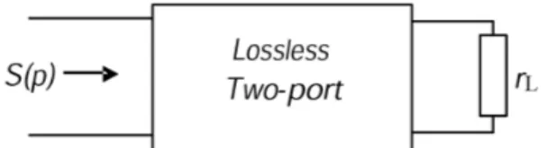
The basic block diagram of a high-pass/low-pass phase shifter can be seen in Figure 1. Detailed analysis and design equations for all-pi topology and hybrid pi/t topology are given in [12] and [19,20], respectively. In [21], three- and five-element all-t and all-pi topologies are studied and element value expressions are given.
Figure 1. High-pass/low-pass phase shifters.
There are numerous studies in the literature about different topologies of high-pass/low-pass phase shifters. In all of these works, high-pass and low-pass section topologies are fixed at the beginning of the study, and then element value expressions are derived for these fixed topologies. However, in the proposed approach, the designer does not fix high-pass and low-pass section topologies; rather, they are fixed as a natural consequence of the proposed approach. In addition, there is no need to derive element value expressions.
In this paper, an algorithm based on the real frequency technique is proposed to design high-pass and low-pass sections of a 0◦–360◦ wide range phase shifter (Figure 1). Since high-pass and low-pass sections are considered as lossless two-ports, the scattering description of lossless two-ports is summarized as a first step. Following this, the proposed algorithm is presented and illustrated with an example.
The proposed approach can easily be adapted to design distributed or mixed (lumped and distributed) element high-pass/low-pass phase shifters [22].
The main topic of this paper is how to design high-pass and low-pass sections of the phase shifter, and not about designing the shifter completely. Therefore, the switching process is not considered in this work.
2. Characterization of lossless two ports
For a lossless two-port with lumped elements, like the one shown in Figure 2, the scattering matrix can be written as [23]:
Figure 2. Lossless two-port terminated by resistance rL.
S(p) = [ S 11(p) S12(p) S21(p) S22(p) ] = 1 g(p) [ h(p) µ f (−p) f (p) −µ h(−p) ] (1)
where g(p), h(p) , and f (p) are real polynomials in complex frequency p = σ + jω ; µ is a constant; and g(p) is a strictly Hurwitz polynomial. The three polynomials g(p), h(p) , and f (p) are related to the Feldtkeller equation as follows:
g(p)g(−p) = h(p)h(−p) + f(p)f(−p) (2)
If the two-port is reciprocal, then the polynomial f (p) is either even or odd. In this case, µ = +1 if f (p) is even, and µ =−1 if f(p) is odd. As a result, for a lossless reciprocal two-port
µ = f (−p)
f (p) =±1 (3a)
and the Feldtkeller equation can be modified as:
g(p)g(−p) = h(p)h(−p) + µ f(p)2. (3b)
From Eq. (1), the transfer scattering coefficient S21(p) is written as:
S21(p) =
f (p)
g(p) (4)
where the polynomial f (p) is formed by using the transmission zeros of the two-port.
Suppose that the desired phase shift in the frequency band of operation is Φ degrees and that the desired amplitude of S21(jω) is unity. Namely, at the end of the section design, the following expression must be
satisfied in the frequency band of operation:
S21(jω) = 1· ∠Φ◦ (5)
The polynomial g(p) can be constructed with Eq. (2) as a strictly Hurwitz polynomial if the polynomial f (p) is formed by the designer, and if the polynomial h(p) is initialized. Therefore, before obtaining the desired phase shift and amplitude response, the initialized polynomial h(p) is optimized.
Suppose the need is to design the low-pass section. By using this section, phase shifts from 0◦ to –180◦ can be obtained [24–26]. In this case, the polynomial f (p) can simply be defined as f (p) = 1 for a ladder network. Then, it can be concluded that
S21(jω) = f (jω) g(jω) = 1· ∠0◦ |g(jω)| ∠g(jω)= 1 |g(jω)|∠ − g(jω) = 1 · ∠Φ◦ (6)
Thus, we have two conditions to check during the optimization process such that
|g(jω)| = 1 (7)
∠g(jω) = −Φ◦
Suppose that we now want to design the high-pass section. In this case the polynomial f (p) can be defined simply as f (p) = pn for a ladder network, where n is the degree of the section. Then:
S21(jω) =
f (jω) g(jω) =
|f(jω)| ∠f(jω)
If the degree n is equal to unity ( n = 1) , then we have S21(jω) = f (jω) g(jω) = jω |g(jω)| ∠g(jω)= ω∠90◦ |g(jω)| ∠g(jω).
Thus, we have two conditions:
|g(jω)| = ω (9)
∠g(jω) = 90◦− Φ◦
If the degree is two ( n = 2) , then the following conditions are obtained:
|g(jω)| = ω2 (10)
∠g(jω) = 180◦− Φ◦
If the degree is three ( n = 3) , then the following conditions are obtained:
|g(jω)| = ω3 (11)
∠g(jω) = −90◦− Φ◦
If the degree is four ( n = 4) , then the following conditions are obtained:
|g(jω)| = ω4 (12)
∠g(jω) = −Φ◦
For higher degrees, the same angle conditions are obtained. For instance, for degree five, it is necessary to check Eq. (9b), and, for degree six, to check Eq. (10b), and so on. However, for an amplitude condition for degree
n , the following expression must be checked:
|g(jω)| = ωn (13)
By using this section, phase shifts from 0◦ to +180◦ can be obtained [24–26].
As a result, high-pass and low-pass sections of a 0◦–360◦ wide range phase shifter can be designed. In the following section, a proposed algorithm based on the real frequency technique is given.
3. Proposed design algorithm Inputs:
• Φ : desired phase shift in degrees.
• ωL = 2π fL and ωH = 2π fH: lower and upper frequencies of the band where Φ degree phase shift is
desired.
• n : desired number of elements in the HP or LP sections.
• f0 or fn: for a low-pass section: f (p) = f0= 1 , and for a high-pass section: f (p) = fn= pn.
• fnorm and Rnorm: frequency and impedance normalization number, respectively.
• k : number of sample frequencies in the band.
• δ : the stopping criterion of the sum of the square errors. Computational steps:
Step 1: Normalize the frequency band as follows: ωL(normalized) = fnormfL and ωH(normalized) = fnormfH .
Calculate the step size ( ss) and the sample frequencies in the band as follows: ss = ωH(normalized)−ωL(normalized)
k+1 ,
ωi= ωL(normalized)+ a· ss, where a = 1, 2, . . . , k .
Step 2: Calculate polynomial g (p) from Eq. (2) briefly since h (p) is initialized and f (p) is selected. This would then mean that the even polynomial g (p)g(−p) is known. Thus, the left-hand side roots of
g (p)g(−p) can be used to form the strictly Hurwitz polynomial g (p).
Step 3: Check Eq. (7) for a low-pass section. Calculate the error via the following expression:
δc=
∑
(1− |g(jω)|)2+∑(Φ◦+∠g(jω))2.
Check Eqs. (9), (10), (11), or (12) according to the degree of the section for the high-pass case. If the degree is unity, then the error is the following:
δc=
∑
(ω− |g(jω)|)2+∑(Φ◦− 90◦+∠g(jω))2.
If the degree is two, then the error is the following:
δc=
∑ (
ω2− |g(jω)|)2+∑(Φ◦− 180◦+∠g(jω))2.
If the degree is three, then the error is the following:
δc =
∑ (
ω3− |g(jω)|)2+∑(Φ◦+ 90◦+∠g(jω))2.
If the degree is four, then the error is the following:
δc =
∑ (
ω4− |g(jω)|)2+∑(Φ◦+∠g(jω))2.
For higher degrees, error expressions can be formed by following the explanations given in Section 2. Step 4: If δc≤ δ , synthesize the corresponding impedance function Z(p) =
1+S11(p) 1−S11(p) =
g(p)+h(p) g(p)−h(p). Now,
it is necessary to denormalize the element values as: L = LnRnorm 2π fnorm , C =
Cn
2π fnormRnorm, and RL = rLRnorm
where Ln, Cn, and rL are normalized inductor, capacitor, and load resistor values, respectively. If δc > δ , go
to Step 5; otherwise, stop.
Step 5: Change the initial coefficients of polynomial h (p) via any optimization routine (in the example, a nonlinear least square optimization routine is used) and go to Step 2.
4. Examples 4.1. Example 1
In this example, the high-pass and low-pass sections of a 5-element 180◦ phase shifter are designed.
For the low-pass section, the polynomial f (p) is f (p) = 1 , and all transmission zeros are put to infinity. The desired number of elements in this section is five, namely n = 5 . Thus, the structure of the polynomial
h (p) is h (p) = h5p5+ h4p4+ h3p3+ h2p2+ h1p + h0. Furthermore, the section should be symmetric; thus, h (p)
must be an odd polynomial. The odd coefficients are selected as h5=−0.01, h3=−0.01, and h1=−0.01.
After applying the proposed algorithm, the following polynomials are obtained:
h (p) =−0.02375p5−0.0096p3−0.0099p, g(p) = 0.02375p5+0.1597p4+0.5465p3+1.1597p2+1.5230p+1, f (p) = 1.
Subsequently, the input impedance expression Z(p) = 1+S11(p) 1−S11(p) =
1+h(p)/g(p)
1−h(p)/g(p) is formed and synthesized.
Normalized element values are calculated as L1= L2= 0.75653 , C1= C3= 0.2975 , C2= 0.93792 .
We are now able to design the high-pass section. The desired number of elements in this section is also five, namely n = 5 . Therefore, the structure of the polynomial h (p) is again h (p) = h5p5+ h4p4+ h3p3+
h2p2+ h1p + h0. This section also needs to be symmetric; therefore, h (p) must be an even polynomial. The
even coefficients are selected as h4 = 0.01 , h2 = 0.01 , and h0 = 0.01 . Since this section is to be a high-pass
type, the polynomial f (p) is f (p) = p5.
After applying the proposed algorithm, the following polynomials are obtained:
h (p) = 0.4178p4+0.4060p2+1, g(p) = 42.0964p5+64.1124p4+48.8191p3+23.0038p2+6.7228p+1, f (p) = p5.
After this, the input impedance expression Z(p) = 1+S11(p) 1−S11(p) =
1+h(p)/g(p)
1−h(p)/g(p) is formed and synthesized. Normalized
element values are calculated as: C4= C6= 3.3614 , C5= 1.0662 , L3= L4= 1.3218 .
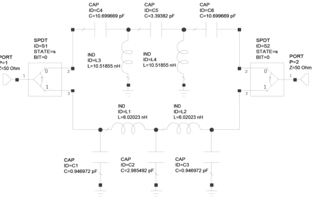
If the calculated normalized element values are denormalized via fnorm = 1GHz and Rnorm = 50Ω ,
the network seen in Figure 3 is obtained. The calculated real element values for low-pass and high-pass cases are L1 = L2 = 6.02nH , C1 = C3 = 0.94pF , C2 = 2.98pF and C4 = C6 = 10.69pF , C5 = 3.39pF ,
L3= L4= 10.51nH , respectively.
Following the procedure introduced in [13,27], design equations for the element values of 5-element high-pass and low-high-pass sections can be obtained. The same phase shifter is designed in [28] via the design equations presented in [28]. The real element values obtained for the low-pass and high-pass cases are L1= L2= 5.49nH ,
C1 = C3 = 1.32pF , C2 = 2.64pF and C4 = C6 = 7.68pF , C5 = 3.84pF , L3 = L4 = 11.25nH , respectively.
The phase shift responses of the phase shifters designed here and given in [28] are compared in Figure 4. The result is that the designed phase shifter has a phase error of 15◦ over an octave bandwidth while the phase shifter given in [28] has a phase error of 14◦.
Figure 3. Designed 5-element 180◦ phase shifter.
The simulated |S11| and |S22| for the designed phase shifter are depicted in Figure 5. Return losses
better than 18 dB for both states are observed over an octave bandwidth.
Figure 4. Phase shift comparison of the 5-element 180◦
phase shifter.
Figure 5. Simulated |S11| and |S22| of the designed
5-element 180◦ phase shifter.
4.2. Example 2
In this example, the high-pass and low-pass sections of a 3-element 45◦ phase shifter have been designed. For the low-pass section, the polynomial f (p) is f (p) = 1 , and all transmission zeros are put to infinity. The desired number of elements in this section is three, namely n = 3 . Therefore, the structure of the polynomial
h (p) is h (p) = h3p3+ h2p2+ h1p + h0. In addition, the section needs to be symmetric; thus, h (p) must be an
After applying the proposed algorithm, the following polynomials are obtained:
h (p) = 0.064p3+ 0.1045p, g(p) = 0.064p3+ 0.2923p2+ 0.7717p + 1, f (p) = 1.
Then, an input impedance expression of Z(p) = 1+S11(p) 1−S11(p) =
1+h(p)/g(p)
1−h(p)/g(p) is formed and synthesized. Normalized
element values are calculated as L1= L2= 0.43815 and C1= 0.66716 .
We can now design the high-pass section. The desired number of elements in this section is also three, namely n = 3 . As a result, the structure of the polynomial h (p) is again h (p) = h3p3+ h2p2+ h1p + h0.
The section again needs to be symmetrical; therefore, h (p) must be an even polynomial. The even coefficients are selected as h2=−0.1 and h0=−0.1. Since this section is to be a high-pass type, the polynomial f(p) is
f (p) = p3.
After applying the proposed algorithm, the following polynomials are obtained:
h (p) = 0.9971p2+ 1, g(p) = 16.4893p3+ 12.6597p2+ 4.8296p + 1, f (p) = p3.
An input impedance expression of Z(p) = 1+S11(p) 1−S11(p) =
1+h(p)/g(p)
1−h(p)/g(p) is then formed and synthesized. Normalized
element values are calculated as: C2 = C3= 2.4148 , L3= 1.4139 . The designed phase shifter is presented in
Figure 6.
Figure 6. Designed 3-element 45◦ phase shifter.
The same phase shifter is designed in [26] via the design equations given in [26]. The normalized element values obtained for the low-pass and high-pass sections are L1= L2= 0.414 , C1= 0.707 and C2= C3= 2.414 ,
L3= 1.41 , respectively.
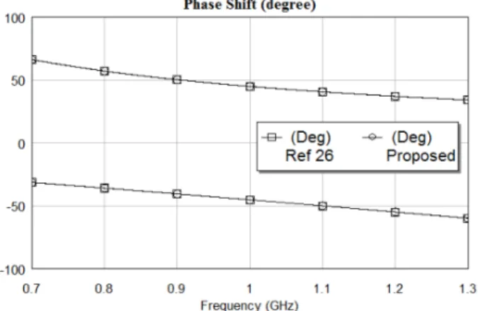
The phase variations of the high-pass and low-pass sections designed here and given in [26] are compared in Figure 7. They are exactly the same in both cases. Therefore, over 10% bandwidth, the phase shift varies from 47◦ down to 43◦ (45◦± 2◦) as shown in [26].
The simulated |S11| and |S22| for the designed phase shifter are depicted in Figure 8. Return losses
better than 20 dB for both states are observed over an octave bandwidth.
Figure 7. Phase shift comparison of the 3-element 45◦
phase shifters for the low-pass and high-pass states.
Figure 8. Simulated |S11| and |S22| of the designed
3-element 45◦ phase shifter.
The phase shifters obtained in both examples were simulated via Microwave Office by Applied Wave Research Inc. (www.awrcorp.com). In the simulation, two single-pole, double-throw switches are used to switch between the low-pass and high-pass states.
5. Conclusion
This study used a real frequency technique-based algorithm to design high-pass and low-pass sections of a lumped-element broadband phase shifter. As mentioned earlier, there are many studies in the literature about different topologies of high-pass/low-pass phase shifters. In all of these works, high-pass and low-pass section topologies are fixed at the beginning of the study and then element value expressions are derived. If a new topology is used, element value expressions must be derived first. However, in the proposed approach, the designer did not fix high-pass and low-pass section topologies; rather, they were natural consequence of the proposed approach. There was no need to derive element value expressions.
In the examples, since symmetric sections were desired, some of the coefficients of polynomial h (p) were restricted. Otherwise, all of the coefficients were free. As a result, a very simple and straightforward method was proposed to design lumped-element high-pass and low-pass sections of a broadband phase shifter circuit. This method can be considered an important tool for many applications such as antenna arrays.
Acknowledgment
Fruitful discussions with A Kummert (Wuppertal, Germany) are gratefully acknowledged. This work was supported in part by Deutscher Akademischer Austauschdienst (DAAD) (A1309962Ref.314).
References
[1] Stark L. Microwave theory of phased-array antennas-A review. P IEEE 1974; 12: 1661-1701. [2] Allen JL. Array antennas: New applications for an old technique. IEEE Spectrum 1964; 1: 115-130. [3] Johnson RC, Jasik H. Antenna Engineering Handbook. 2nd ed. New York, NY, USA: McGraw-Hill, 1984.
[4] Alonso JI, Blas JM, Garcia LE, Ramos J, Pablos J, Grajal J, Gentili GG, Gismero J, Perez F. Low cost electronically steered antenna and receiver system for mobile satellite communications. IEEE T Microw Theory 1996; 44: 2438-2449.
[5] Edward BJ, Webb RS, Weinreb SA. W-band active phased-array antenna. Microwave J 1996; 254-262.
[6] Viverios D, Conconmi D, Jastrzebski AK. A Tunable all-pass MMIC active phase shifter. IEEE T Microw Theory 2002; 50: 1885-1889.
[7] Gupta RK, Estep GC, Upshur JI. MMIC techniques for active phased-array antenna systems for future communi-cations satellites. In: Asia-Pacific Microwave Conference; 6–9 December 1994; Tokyo, Japan. pp. 897-902.
[8] Hirshfield E. The global system. Appl Microw 1996; 91-99.
[9] Johannsen KG. Mobile P-service satellite system comparison. Int J Satell Commun 1995; 13: 453-462.
[10] Kang DW, Lee H, Lee K. Design of a phase shifter with improved bandwidth using embedded series-shunt switches. In: European Microwave Conference; 4–6 October 2005; Paris, France. pp. 311-314.
[11] Onno P, Pitkins A. Miniature multi-kilowatt PIN diode MIC digital phase shifters. In: IEEE GMTT International Microwave Symposium Digest; 16–19 May 1971; Washington, DC, USA. New York, NY, USA: IEEE. pp. 22-23. [12] Morton MA, Comeau JP, Cressler JD. Source of phase error and design considerations for silicon-based monolithic
high-pass/low-pass microwave phase shifters. IEEE T Microw Theory 2006; 54: 4032-4040. [13] Garver RV. Broad-band diode phase shifters. IEEE T Microw Theory T 1972; 20: 314-323.
[14] Kingsley N, Papapolymerou J. Organic wafer-scale packaged miniature 4-bit RF MEMS phase shifter. IEEE T Microw Theory 2006; 54: 1229-1236.
[15] Malczewski A. X-band RF MEMS phase shifters for phased array applications. IEEE Microw Wirel Co 1999; 9: 517-519.
[16] Hayden JS. Very low-loss distributed X-band and Ka-band MEMS phase shifters using metal-air-metal capacitors. IEEE T Microw Theory 2003; 51: 309-314.
[17] Hancock TM, Rebeiz GM. A 12-GHz SiGe phase shifter with integrated LNA. IEEE T Microw Theory 2005; 53: 977-983.
[18] Tayrani R, Teshiba MA, Sakamoto GM, Chaudhry Q, Alidio R, Yoosin K, Ahmad IS, Cisco TC, Hauhe M. Broad-band SiGe MMICs for phased-array radar applications. IEEE J Solid-St Circ 2003; 38: 1462-1470.
[19] Morton MA, Comeau JP, Cressler JD, Mitchell M, Papapolymerau J. 5 bit silicon-based X-band phase shifter using a hybrid pi/t high-pass/low-pass topology. IET Microw Antenna P 2008; 2: 19-22.
[20] Tang X, Mouthaan K. Design considerations for octave-band phase shifters using discrete components. IEEE T Microw Theory 2010; 58: 3459-3466.
[21] Chen L, Bai Y, Xing X. Performance of high-/low-pass phase shifter in broadband. In: IEEE International Conference on Ultra-Wideband; 20–23 September 2010; Nanjing, China. New York, NY, USA: IEEE. pp. 1-4. [22] Richards PI. Resistor-terminated-line circuits. Proc IRE 1948; 36: 217-220.
[23] Belevitch V. Classical Network Theory. San Francisco, CA, USA: Holden Day, 1968.
[24] Yarman BS. Novel circuit configurations to design loss balanced 0◦–360◦ digital phase shifters. Int J Electron Commun 1991; 45: 96-104.
[25] Yarman BS. New approaches to design digital phase shifters over the complete phase plane. Medical Journal of the Islamic World Academy of Sciences 1991; 4: 14-25.
[26] Yarman BS. New circuit configurations for designing 0◦–180◦ digital phase shifters. IEE P 1987; 134: 253-260. [27] Adler A, Popovich R. Broadband switched-bit phase shifter using all-pass networks. In: IEEE MTT-S International
Microwave Symposium Digest; 10–14 July 1991; Boston, MA, USA. New York, NY, USA: IEEE. pp. 265-268. [28] Tang X, Mouthaan K. A broadband 180◦ phase shifter with a small phase error using lumped elements. In: Asia