BilRC: An Execution Triggered Coarse Grained
Reconfigurable Architecture
Oguzhan Atak and Abdullah Atalar, Fellow, IEEE
Abstract— We present Bilkent reconfigurable computer (BilRC), a new coarse-grained reconfigurable architecture (CGRA) employing an execution-triggering mechanism. A control data flow graph language is presented for mapping the appli-cations to BilRC. The flexibility of the architecture and the computation model are validated by mapping several real-world applications. The same language is also used to map applications to a 90-nm field-programmable gate array (FPGA), giving exactly the same cycle count performance. It is found that BilRC reduces the configuration size about 33 times. It is synthesized with 90-nm technology, and typical applications mapped on BilRC run about 2.5 times faster than those on FPGA. It is found that the cycle counts of the applications for a commercial very long instruction word digital signal processor processor are 1.9 to 15 times higher than that of BilRC. It is also found that BilRC can run the inverse discrete cosine transform algorithm almost 3 times faster than the closest CGRA in terms of cycle count. Although the area required for BilRC processing elements is larger than that of existing CGRAs, this is mainly due to the segmented interconnect architecture of BilRC, which is crucial for supporting a broad range of applications.
Index Terms— Coarse-grained reconfigurable architectures
(CGRA), discrete cosine transform (DCT), fast Fourier transform (FFT), reconfigurable computing, turbo decoder, Viterbi decoder.
I. INTRODUCTION
T
O COMPLY with the performance requirements of emerging applications and evolving communication standards, various architecture alternatives are available. Field-programmable gate arrays (FPGAs) lack run-time programmability, but they compete with their large number of logic resources. To maximize the device utilization, FPGA designers partition the available resources among several sub-applications in such a manner that each application works at the chosen clock frequency and complies with the throughput requirement. The design phases of FPGAs and application-specific integrated circuits (ASICs) are quite similar except that ASICs lack post-silicon flexibility.Unable to exploit the space dimension, digital signal proces-sors (DSPs) fail to provide the performance requirement of many applications due to the limited parallelism that a sequen-tial architecture can provide. This limitation is not due to the Manuscript received June 28, 2011; revised April 24, 2012; accepted June 12, 2012. Date of publication July 31, 2012; date of current version June 21, 2013.
The authors are with the Department of Electrical and Elec-tronics Engineering, Bilkent University, Ankara 06800, Turkey (e-mail: [email protected]; [email protected]).
Color versions of one or more of the figures in this paper are available online at http://ieeexplore.ieee.org.
Digital Object Identifier 10.1109/TVLSI.2012.2207748
area cost of logic resources, but to lack of a computation model to exploit such a large number of logic resources. Commercial DSP vendors produce their DSPs with several accelerators. The disadvantage of such an approach is its inability to adapt to emerging applications and evolving standards.
Application-specific instruction-set processors (ASIP) provide high performance with dedicated instructions having very deep pipelines. An ASIP [1] with a 15-pipeline stage is presented for various Turbo and convolutional code standards. A multiASIP [2] architecture is presented for exploiting different parallelism levels in the Turbo decoding algorithm. In a previous work, we presented ASIPs having dedicated instructions and a memory architecture for speeding up fast Fourier transform (FFT) [3]. The basic limitation of the ASIP approach is its weak programmability, which makes it inflexible for emerging standards. For instance, aforementioned ASIPs do not support Turbo codes with more than eight states [2] and 16 states [1].
Coarse-grained reconfigurable architectures (CGRAs) have been proposed to provide a better performance/flexibility balance than the alternatives discussed above. Hartenstein [4] compared several CGRAs according to their interconnection networks, data path granularities, and application mapping methodologies. In a recent survey paper, De Sutter et al. [5] classified several CGRAs according to computation models while discussing the relative advantages and disadvantages. Compton et al. [6] discussed reconfigurable architectures containing heterogeneous computation elements, such as CPU and FPGA, and compared several fine- and coarse-grained architectures with partial and dynamic configuration capa-bility. According to the terminologies in the literature [4]–[6], RA, including FPGAs, can be classified according to the configuration in three distinct models as single-time config-urable, statically reconfigconfig-urable, and dynamically reconfig-urable. Statically reconfigurable RAs are configured at loop boundaries, whereas dynamic RAs can be configured at almost each clock cycle. The basic disadvantage of statically recon-figurable RAs is that if the loop to be mapped is larger than the array size, it may be impossible to map. However, the degree of parallelism inside the loop body can be decreased to fit the application to CGRA. This is the same approach that designers use for mapping applications to an FPGA. In dynamically reconfigurable RAs, the power consumption can be high due to fetching and decoding of the configuration at every clock cycle; however, techniques have been proposed [7] to reduce power consumption due to dynamic configuration. The interconnect topology of RAs can be either 1-D, such 1063-8210/$31.00 © 2012 IEEE
as PipeRench [8] and RAPID [9], [10] or 2-D, such as ADRES [11]–[15], MorphoSys [16], MORA [17], [18], and conventional FPGAs.
RAs can have a point-to-point (p2p) interconnect structure as in ADRES, MORA, MorphoSys, and PipeRench or a segmented interconnect structure as in KressArray, RAPID, and conventional FPGAs. p2p interconnect has the advantage of deterministic timing performance. The clock frequency of the RA does not depend on the application mapped while the fan-out of the processing elements (PEs) is limited. Limited p2p interconnect may increase the initiation interval [13] and cause performance degradation. For the segmented intercon-nect method, the output of a PE can be routed to any PE, while the timing performance depends on the application mapped.
The execution control mechanism of RAs can be either of a statically scheduled type, such as MorphoSys and ADRES, where the control flow is converted to data flow code during compilation, or a dynamically scheduled type, such as KressArray, which uses tokens for execution control.
In this paper, we present Bilkent reconfigurable computer (BilRC),1 a statically reconfigurable CGRA with a 2-D segmented interconnect architecture utilizing dynamic scheduling with execution triggering. Our contributions can be summarized as follows.
1) An execution triggered computation model is presented, and the suitability of the model is validated with several real world applications. For this model, a language for reconfigurable computing (LRC), is developed.
2) A new CGRA employing segmented interconnect archi-tecture with three types of PEs and its configuration architecture is designed in 90-nm CMOS technology. The CGRA is verified up to the layout level.
3) Full tool flow, including a compiler for LRC, a cycle accurate SystemC simulator, and a placement & routing tool for mapping applications to BilRC is developed. 4) The applications modeled in LRC are converted to HDL
with our LRC-HDL converter and then mapped onto an FPGA and to BilRC on a cycle-by-cycle equivalent basis. Then, a comparison of precise configuration size and timing is done.
II. BILRC ARCHITECTURE
BilRC has three types of PEs: arithmetic logic unit (ALU), memory (MEM), and multiplier (MUL). Similar to some commercial FPGA architectures, such as Stratix2 and Virtex3 PEs of the same type are placed in the same column as shown in Fig. 1. The architecture repeats itself every nine columns and the number of rows can be increased without changing the distribution of PEs. This PE distribution is obtained by considering several benchmark algorithms from signal and image processing and telecommunication applications. The PEs’ distribution can be adjusted for better utilization for the targeted applications. For example, the Turbo decoder algorithm does not require any multiplier, but needs a large
1BilRC: Bilkent reconfigurable computer. 2Available at http://www.altera.com. 3Available at http://www.xilinx.com.
Fig. 1. Columnwise allocation of PEs in BilRC.
amount of memory. On the other hand, filtering applications require many multipliers, but not much memory. For the same reason, commercial FPGAs have different families for logic-intensive and signal processing-intensive applications.
A. Interconnect Architecture
PEs are connected to four neighboring PEs [3] by commu-nication channels. Channels at the periphery of the chip can be used for communicating with the external world. If the number of ports in a communication channel is Np, the total
number of ports a PE has is 4Np. The interconnect architecture
is the same for all PE types. Fig. 2(a) illustrates the signal routing inside a PE for Np = 3. There are three inputs and
three outputs on each side. The output signals are connected to corresponding input ports of the neighbor PEs. The input and output signals are all 17 bits wide. 16 bits are used as data bits and the remaining execute enable (EE) bit is used as the control signal.
PEs contain processing cores (PC) located in the middle. Port route boxes (PRB) at the sides are used for signal routing. PCs of ALUs and MULs have two outputs and the PC of MEM has only one output. The second output of a PC is utilized for various purposes, such as the execution control for loop instructions, the carry output of additions, the most significant part of multiplication, the maximum value of index calculation, and the conditional execution control. PC outputs are routed to all PRBs. Therefore, any PRB can be used to route PC output in the desired direction. All input signals are routed to all PRBs and to the PC as shown in Fig. 2(a). The PC selects its operands from the input signals by using internal multiplexers. Fig. 2 shows the internal structure of PRB. The route multiplexer is used to select signals coming from all input directions and from the PC. The pipeline multiplexer is used to optionally delay the output of the route multiplexer for one clock cycle. BilRC is configured statically, hence both the interconnects and the instructions programmed in PCs remain unchanged during the run.
Fig. 3 shows an example mapping. PE1 is the source PE and PE4 is the destination PE, while PE2 and PE3 are used for signal routing. The total delay, TCRIT, between the register in PE1 and the register in PE4 is given as
Fig. 2. PE architecture. (a) Input/output signal connections. (b) Schematic diagram of PRB.
Fig. 3. Example of routing between two PEs.
where n = 2 is the number of hops, THOP is the time delay to traverse one PE, and TP E is the time delay within a PE.
B. PC Architectures
1) MEM: Fig. 4 shows the architecture of the PC of MEM.
PC has a data bus which is formed from all input data signals and an EE bus which is formed from all input EE signals. SRAM block in PC is a 1024 × 16 dual port RAM (ten address bits, 16 data bits). op1_addr set by the configuration register (CR) determines which one of the 12 inputs is the read address. Similarly, op2_addr chooses one of the inputs as the write address. The most significant six bits are compared with MEMID stored in the CR. If they are equal, then read and/or write operations are performed. opr3_addr selects the data to be written from one of the input ports.
2) ALU: Fig. 5 shows the architecture of ALU. Similar to
MEM, ALU has two buses for input data and EE signals. The operands to the instructions are selected from the data bus by using the multiplexers M3, M4, M5, M6. ALU has an 8× 16 register file for storing constant data operands. For example, an ALU with the instruction, ADD(A, 100) reads the variable A from an input port, and the constant 100 is stored in the register file during configuration. The output of the register file is connected to the data bus so that the instruction can select its operand from the register file. The execution of the instruction is controlled from the EE bus. The CR has a field
Fig. 4. PC schematic of MEM.
Fig. 5. PC schematic of ALU.
to select the input EE signal from the EE bus. PC executes the instruction when the selected signal is enabled.
3) MUL: The PC of MUL is similar to that of ALU.
The difference is the instructions supported in the two types of PEs. Multiplication and shift instructions are performed in this PE. The MUL instruction performs the multiplication operation on two operands. The operands can be from the
TABLE I
CONFIGURATIONDATASTRUCTURE
Conf. item Number of words Meaning PID 1 PID
N 1 Number of words in theconfiguration packet
CR 3 PC CR RCR 5 It is used to configure multiplexers in the PRBs output initialization register
1 Loads the register foroutput initialization
Register file or memory content
configuration
variable
The register file of ALU or MEM or the SRAM of the MEM is initialized
inputs (variable operands) or from the register file (constant operands). The result of the multiplication is a 32-bit number that appears on two output ports. Alternatively, the result of the multiplication can be shifted to the right in order to fit the result to a single output port by using the MUL_SHR (multiply and shift to the right) instruction. This instruction executes in two clock cycles: the multiplication is performed in the first clock cycle and the shifting is performed in the second clock cycle. The rest of the instructions for all PEs are executed in a single clock cycle.
C. Configuration Architecture
PEs are configured by configuration packets, which are composed of 16-bit configuration words. Table I lists the data structure of the configuration packet. Each PE has a 16-bit-wide configuration input and a configuration output. These signals are connected in a chain structure as shown in Fig. 1. The first word of the configuration packet is the processing element ID (PID). A PE receiving the configuration packet uses it if the PID matches its own ID. The second word in the packet is the length of the configuration packet. The fields of the CR are illustrated in Table II for ALU. The CR of MEM does not require the fields opr4_addr, EE_addr, Init_Addr, Init_type, and Init_Enable, and the CR of MUL does not contain the opr4_addr field, since none of the instructions require four operands. CR is 48 bits long for all PC types; the unused bit positions are reserved for future use. It must be noted that the bit width of the CR and route CR depends on Np. The number of words for the fields given
in the table is for Np= 4.
III. EXECUTION-TRIGGEREDCOMPUTATIONMODEL Writing an application in a high-level language, such as C and then mapping it on the CGRA fabric is the ultimate goal for all CGRA devices. To get the best performance from the CGRA fabric, a middle-level language (assembly-like language) that has enough control on PEs and provides abstractions is necessary. The designers thus do not deal with unnecessary details, such as the location of the instructions in the 2-D architecture and the configuration of route multi-plexers for signal routing. Although there are compilers for
TABLE II ALU CR
Conf. field Number
of bits Meaning opr1_addr 5 Operand 1 address opr2_addr 5 Operand 2 address opr3_addr 5 Operand 3 address opr4_addr 5 Operand 4 address
EE_addr 5 EE input address
Init_addr 4 Initialization input address op_code 8 Selects the instruction to
be executed
Init_Enable 1
Determines whether the PC has an initialization
or not Init_Type 1 Determines the type of
the initialization
some CGRAs, which directly map applications written in a high-level language, such as C to the CGRA, the designers still need to understand the architecture of the CGRA in order to fine tune applications written in C-code for the best performance [5].
The architecture of BilRC is suitable for direct mapping of control data flow graphs (CDFG). A CDFG is the represen-tation of an application in which operations are scheduled to the nodes (PEs) and dependencies are defined. We developed a LRC for the efficient representation of CDFGs. Generating LRC code from a high-level language is outside the scope of this paper. Existing tools, such as IMPACT [14] can be used to generate a CDFG in the form of an intermediate representation called LCode. IMPACT reads a sequential code, draws a data flow graph and generates a representation defining the instructions that are executed in parallel. Such a representation can then be converted to an LRC code.
A. Properties of LRC
1) LRC is a Spatial Language: Unlike sequential languages,
the order of instructions in LRC is not important. LRC instruc-tions have execution control inputs that trigger the execution. LRC can be considered as a graph drawing language in which the instructions represent the nodes and the data, and control operands represent the connections between the nodes.
2) LRC is a Single Assignment Language: During mapping
to the PEs, each LRC instruction is assigned to a single PE. Therefore, the output of the PEs must be uniquely named. A variable can be assigned to multiple values indirectly in LRC by using the self-multiplexer instruction, SMUX.
3) LRC is Cycle Accurate: Even before mapping to the
architecture, cycle-accurate simulations are possible to obtain timing diagrams of the application. Each instruction in LRC, except MUL_SHR, is executed in a single clock cycle.
4) LRC has an Execution-Triggering Mechanism: LRC
instructions have explicit control signal(s), which trigger the execution of instruction assigned to the node. Instructions that are triggered from the same control signal execute concur-rently, hence parallelism is explicit in LRC.
B. Advantages of Execution Triggered Computation Model
The execution-triggered computation model can be compared to the data flow computation model [19]. The basic similarity is that both models build a data flow graph such that nodes are instructions and the arcs between the nodes are operands. The basic difference is that the data flow computation model uses tagged tokens to trigger execution; a node executes when all its operands (inputs) have a token and the tags match. Basically, tokens are used to synchronize operands, and tags are used to synchronize different loop iterations. In LRC, an instruction is executed when its EE signal is active. Application of the data flow computation model to CGRAs has the following problems: first, tagged tokens require a large number of bits; this in turn increase the interconnect area. For example, the Manchester machine [19] uses 54 bits for tagged tokens. Second, a queue is required to store tagged tokens, which increases the area of PE. Third, a matching circuit is required for comparing tags, both increasing PE area and decreasing performance. For example, an instruction with three operands requires two pairwise tag comparisons to be made. Execution-triggered computation uses a single bit as EE, hence it is both area efficient and fast. The execution-triggered computation model can be compared to the computation models of existing CGRAs. MorphoSys [16] uses a RISC processor for the control-intensive part of the application. The reconfigurable cell array is intended for the data-parallel and regular parts of the application. There is no memory unit in the array; instead, a frame buffer is used to provide data to the array. The RISC processor performs loop initiation and context broadcast to the array. Each reconfigurable cell runs the broadcast instructions sequentially. This model has many disadvantages. First, an application cannot be always partitioned into control-intensive and data-intensive parts, and even if it is partitioned, the inter-communication between the array and RISC creates a performance bottleneck. Second, the lack of memory units in the array limits the applications that can be run on the array. Third, since loop initiation is controlled by the RISC processor, the array can be used only for innermost loops. ADRES [14] uses a similar computation model with some enhancements, the RISC processor is replaced with a very long instruction word (VLIW) processor. ADRES is a template CGRA. Different memory hierarchies can be constructed by using the ADRES core. For example, two levels of data caches can be attached to ADRES [15], or a multiported scratch pad memory can be attached [20], [21]. There is no array of data memories in the ADRES core. The VLIW processor is responsible for loop initiation and the control-intensive part of the application. Lack of parallel data memory units in the ADRES core limits the performance of the applications mapped on ADRES. In a recent work on ADRES [20], a four-ported scratchpad memory was attached to the ADRES core for applications requiring parallel memory accesses. In ADRES, the loops are initiated from the VLIW processor. Hence, only a single loop can run at a time. ADRES has a mature tool suite, which can map applications written in C-language directly to the architecture. Obviously, this is a major advantage. The VLIW
processor in the ADRES can also be used for the parts of the applications which require low parallelism.
MORA [18] is intended for multimedia processing. The reconfigurable cells are DSP-style sequential execution proces-sors, which have internal 256-byte data memory for partial results and a small instruction memory for dynamic configu-ration of the cells. The reconfigurable cells communicate with an asynchronous handshaking mechanism. MORA assembly language and the underlying reconfigurable cells are opti-mized for streaming multimedia applications. The computa-tion model is unable to adapt to complex signal processing and telecommunications applications. RAPID [10] is a 1-D array of computation resources, which are connected by a configurable segmented interconnect. RAPID is programmed with RAPID-C programming language. During compilation, the application is partitioned into static and dynamic config-urations. The dynamic control signals are used to schedule operations to the computation resources. A sequencer is used to provide dynamic control signals to the array. The centralized sequencer approach to dynamically change the functionality requires a large amount of control signals, and for some applications the required number of signals would not be manageable. Therefore, RAPID is applicable to highly regular algorithms with repetitive parts.
LRC is efficient from a number of perspectives. First, LRC has flexible and efficient loop instructions. Therefore, no external RISC or VLIW processor is required for loop initia-tion. An arbitrary number of loops can be run in parallel. The applications targeted for LRC are not limited to the innermost loops. Second, LRC has memory instructions to flexibly model the memory requirements of the applications. For example, the Turbo decoding algorithm requires 13 memory units. The access mechanism to the memories is efficiently modeled. The extrinsic information memory in the Turbo decoder is accessed by four loop indices. LRC has also flexible instructions to build larger-sized memory units. ADRES, MorphoSys, and MORA have no such memory models in the array. Third, the execution control of LRC is distributed. Hence, there is no need for an external centralized controller to generate control signals, as is required in RAPID. The instruction set in LRC is flexible enough to generate complex addressing schemes, and no external address generators are required. While LRC is not biased to streaming applications, they can be modeled easily. In a CDFG, every node represents a computation, and connections represent the operands. An example CDFG and timing diagram is shown in Fig. 6. The node ADD performs an addition operation on its two operands Op1_Data and Op2_Data when its third operand, Op3_EE, is activated. Below is the corresponding LRC line
[Res, 0] = ADD (Op1, Op2) < −[Op3].
In LRC, the outputs are represented between the brackets on the left of the equal sign. A node can have two outputs; for this example only the first output, Res, is utilized. A “0” in place of an output means that it is unused. Res is a 17-bit signal that is composed of 16-bit data, Res_Data, and a one-bit EE signal, Res_EE. The name of the function is provided after the equal sign. The operands of the function are given
Fig. 6. Example CDFG and timing diagram.
between the parentheses. The control signal that triggers the execution is provided between the brackets on the right of the “<–” characters. As can be seen from the timing diagram, the instruction is executed when its EE input is active. The execution of an instruction takes one clock cycle; therefore, the Res_EE signal is active one clock cycle after Op3_EE.
C. Loop Instructions
Efficient handling of loops is critical for the performance of most applications. LRC has flexible and efficient loop instructions. By using multiple LRC loop instructions, nested, sequential, and parallel loop topologies can be modeled.
A typical FOR loop in LRC is given as follows: [i, i_Exit] = FOR_SMALLER(StartVal, EndVal, Incr)
< −[LoopStart, Next].
This FOR loop is similar to that in C-language
for(i = StartVal; i < EndVal; i = i + Incr) loop body. The FOR_SMALLER instruction works as follows.
1) When the LoopStart signal is enabled for one clock cycle, the data portion of the output, i_DATA, is loaded with StartVal_DATA, and the control part of the output i_EE is enabled in the next clock cycle.
2) When the Next signal is enabled for one clock cycle, i_DATA is loaded with i_DATA+Incr_DATA and i_EE is enabled if i_DATA+Incr_DATA is smaller than EndVal; otherwise, i_Exit_EE is enabled.
The parameters StartVal, EndVal, and Incr can be variables or constants.
Fig. 7 shows an example CDFG having three nodes. The LRC syntax of the instructions assigned to the nodes is shown at the right of the nodes. All operands of FOR_SMALLER are constant in this example. When mapped to PEs, constant operands are initialized to the register file during configuration. ADD and SHL (SHift Left) instruc-tions are triggered from i_EE. Hence, their outputs k and m are activated at the same clock cycles as illustrated in Fig. 8. The Next input of the FOR_SMALLER tion is connected to the k_EE output of the ADD instruc-tion. Therefore, FOR_SMALLER generates an i value for every two clock cycles. When i exceeds the boundary, FOR_SMALLER activates the i_Exit signal. The trig-gering of instructions is illustrated in Fig. 8 with dotted lines. SFOR_SMALLER is a self-triggering FOR instruction
Fig. 7. CDFG and LRC example for FOR_SMALLER.
Fig. 8. Timing diagram of FOR_SMALLER.
given as
[i, i_Exit] = SFOR_SMALLER(StartVal, EndVal, Incr, IID)
< −[LoopStart].
The SFOR_SMALLER instruction does not require a Next input; but instead it requires a fourth constant operand, inter iteration dependency (IID). SFOR_SMALLER waits for the IDD cycles to generate the next loop index after generating the current loop index. This instruction triggers itself and can generate an index for every clock cycle when IID is 0. LRC has support for loops whose index variables are descending; these instructions are FOR_BIGGER and SFOR_BIGGER. The aforementioned for loop instructions can be used as a while loop by setting the Incr operand to 0. By doing so, it always generates an index value. This is equivalent to an infinite while loop. The exit from this while loop can be coded externally by conditionally activating the next input.
D. Modeling Memory in LRC
In LRC, every MEM instruction corresponds to a 1024-entry, 16-bit, two-ported memory. The syntax for MEM instruction is given below
[Out] = MEM(MemID, ReadAddr, InitFileName, WriteAddr, WriteIN).
The MEM instruction takes five operands. MemID is used to create larger memories as discussed earlier. The ten least significant bits of ReadAddr_Data are connected to the read address port of the memory. When ReadAddr_EE is active, the data in the memory location addressed by ReadAddr_Data is
put on Out_DATA in the following clock cycle and Out_EE is activated. The InitFileName parameter is used for initializing the memory. The write operation is similar to reading. When WriteAddr_EE is active, the data in WriteIN_Data is written to the memory location addressed by WriteAddr_Data. Below is an example for forming a 2048-word memory
1: [Out1] = MEM(0, ReadAddr, File0, WriteAddr, WriteData) 2: [Out2] = MEM(1, ReadAddr, File1,
WriteAddr, WriteData) 3: [Out] = SMUX(Out1, Out2).
The first memory has MemID = 0. This memory responds to both read and write addresses if they are between 0 and 1023; similarly, the second memory responds only to the addresses between 1024 and 2047. Therefore, the signals Out1_EE and Out2_EE cannot both be active in the same clock cycle. The SMUX instruction in the third line multiplexes the operand with the active EE signal. Due to the SMUX instruction, one clock cycle is lost. The SMUX instruction can take four operands. Therefore, up to 4n memories can be merged with
n clock cycles of latency.
E. Conditional Execution Instructions
LRC has novel conditional execution control instructions. Below is a conditional assignment statement in C language
if(A > B) {result = C;} else {result = D;}. Its corresponding LRC code is given as
[c_result, result] = BIGGER(A, B, C, D) < −[Opr]. BIGGER executes only if its EE input, Opr_EE, is active. result is assigned to operand C if A is bigger than B; otherwise it is assigned to D. c_result is activated only if A is bigger than B. Since c_result is activated only if the condition is satisfied, the execution control can be passed to a group of instructions that is connected to this variable. The example C code below contains not only assignments, but also instructions in the if and else bodies
if(A > B) {result = C + 1;} else {result = D − 1;}. This C-code can be converted to an LRC code by using three LRC instructions
1: [Cp1, 0] = ADD(C, 1) < −[C] 2: [Dm1, 0] = SUB(D, 1) < −[D]
3: [0, result] = BIGGER(A, B, Cp1, Dm1) < −[Opr]. The first line evaluates C+1, the second line evaluates D-1, and in the third line, result is conditionally assigned to Cp1 or Dm1 depending on the comparison A > B. Conditional instructions supported in BilRC are as follows: SMALLER, SMALLER_EQ (smaller or equal), BIGGER, BIGGER_EQ (bigger or equal), EQUAL and NOT_EQUAL. By using these instructions, all conditional codes can be efficiently implemented in LRC. ADRES [12] uses a similar
predicated execution technique. In LRC, two branches are merged by using a single instruction. In predicated execution, a comparison is made first to determine the predicate, and then the predicate is used in the instruction. In LRC, the results of two or more instructions cannot be assigned to the same variable since these instructions are the nodes in the CDFG. Therefore, the comparison instructions in LRC are used to merge two branches of instructions. Similar merge blocks are used in data flow machines [19] as well.
F. Initialization Before Loops
1: min = 32767;
2: for(i = 0; i < 255; i + +){ 3: A = mem[i];
4: if(A < min)min = A; 5: }.
In the C-code above, the variable min is assigned twice, before the loop and inside the loop. Such initializations before loops are frequently encountered in applications with recurrent dependencies. Multiple assignment to a variable is forbidden in LRC as discussed in Section III-A2. An initialization technique has been devised for LRC instructions, which removes the need for an additional SMUX instruction.
The corresponding LRC code is given below 1: [i, iExit] = SFORSMALLER(0, 256, 1, 0)
< −[LoopStart]
2: [A, 0] = MEM(0, i, filerand.txt, WriteAddr, WriteData) 3: [min(32767), 0] = MIN(min, 0, A, 0)<−[A, LoopStart]. MIN finds the minimum of its first and third operands.4 The EE input of the MIN instruction is A_EE. The second control signal between the brackets to the right of the “< −” characters, LoopStart, is used as the initialization enable. When this signal is active, the Data part of the first output is initialized. The parentheses after the output signal min represent the initialization value.
G. Delay Elements in LRC
CDFG representation of algorithms requires many delay elements. These delay elements are similar to the pipeline registers of pipelined processors. A value calculated in a pipeline stage is propagated through the pipeline registers so that further pipeline stages use the corresponding data
1: for(i = 0; i < 256; i + +){ 2: A = mem[i]; 3: B = abs(A); 4: C = B >> 1; 5: if(C > 2047)R = 2047; 6: elseR = C; 7: res_mem[i] = R; 8: }.
4The second and fourth operands of MIN are used for the index of minimum calculation.
In the C-code above, the data at location i is read from a memory A, its absolute value is calculated at B, shifted to the right by 1 at C and finally saturated and saved to the memory at location i. Below is the corresponding LRC code:
1: [i, iExit] = SFORSMALLER(0, 256, 1, 0) < −[LoopStart]
2: [A, 0] = MEM(0, i, filerand.txt, 0, 0) 3: [B, 0] = ABS(A) < −[A]
4: [C, 0] = SHR(B, 0, 1) < −[B]
5: [0, R] = BIGGER(C, 2047, 2047, C) < −[C] 6: [mem2, 0] = MEM(0, 0, 0, i(4), R).
Although, the LRC instructions are written here in the same order as in the C-code, this is not necessary. The order of instructions in LRC is not important. The IID operand of the SFOR_SMALLER instruction is set to 0. Therefore, an index value, i, is generated from 0 to 255 at every clock cycle. After six clock cycles, all the instructions are active at each clock cycle until the loop boundary is reached. Since the instructions are pipelined, the MEM instruction above cannot use i as the write address, but its four-clock-cycle delayed version. The number of pipeline delays is coded in LRC by providing it between the parentheses following the variable. The requirement to specify delay value explicitly in LRC for pipelined designs makes code development a bit difficult. However, the difficulty is comparable to that of designing with HDL or assembly languages.
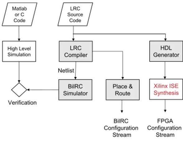
IV. TOOLS ANDSIMULATIONENVIRONMENT Fig. 9 illustrates the simulation and development environ-ment. The four key components are the following.
1) LRC Compiler: Takes the code written in LRC and
generates a pipelined netlist. The net has the following infor-mations: input connection, output connection, the number of pipeline stages between the input and the output.
2) BilRC Simulator: Performs cycle-accurate simulation of
LRC code. The BilRC simulator is written in System C.5The pipelined netlist is used as the input to the BilRC simulator. PCs are interconnected according to the nets. If a net in the netlist file has delay elements, then these delay elements are inserted between PCs. The results of a simulation can be observed in three ways: from the SystemC console window, the value change dump (VCD) file, or the BilRC log files. Every PC output has been registered to SystemC’s built-in function sc_trace; thus by using a VCD viewer all PC output signals can be observed in a timing diagram.
3) Placement & Routing Tool: This tool maps the nodes
of CDFGs into a 2-D architecture, and finds a path for every net. Unlike FPGAs’, the interconnection network of BilRC is pipelined. The BilRC place & route tool finds the location of the delay elements during the placement phase. The placement algorithm uses the simulated annealing technique with a cooling schedule adopted from [22]. The total number of delay elements that can be mapped to a node is 4Np.
5Available at http://www.systemc.org/home/.
Fig. 9. Simulation and implementation environment.
For every output of a PC, a pipelined interconnect is formed. When placing the delay elements, contiguous delay elements are not assigned to the same node. Such movements in the simulated annealing algorithm are forbidden. A counter is assigned for every node, which counts the number of delay elements assigned to the node. The counter values are used as a cost in the algorithm. Therefore, delay elements are forced to spread around the nodes. The placement algorithm uses the shortest path tree algorithm for interconnect cost calculation. The algorithm used for routing is similar to that of the negotiation based router [23].
4) HDL Generator: Converts LRC code to HDL code.
Since LRC is a language to model CDFGs, it is easy to generate the HDL code from it. For each instruction in LRC, there is a pre-designed VHDL code. The HDL generator connects the instructions according to the connections in the LRC code. The unused inputs and outputs of instructions are optimized during HDL generation. The quality of the generated HDL code is very close to that of manual coded HDL. The generated HDL code can then be used as an input to other synthesis tools, such as the Xilinx ISE. The generated HDL code was used to map applications to an FPGA in order to compare the results with LRC code mapped to BilRC.
V. EXAMPLEAPPLICATIONS FORBILRC
In order to validate the flexibility and efficiency of the proposed computation model, several standard algorithms selected from Texas Instruments benchmarks [24] are mapped to BilRC. We also mapped Viterbi and Turbo decoder channel decoding algorithms and multirate and multichannel FIR filters. For all cases, it is assumed that the input data are initialized into the memories and the outputs are directly provided to the device outputs. Due to space restrictions, only some of the algorithms will be discussed. In Section V-A, use of the loop exit signal to trigger the rest of the code is demon-strated. In the second example, a matrix transposition and pipelining of horizontal and vertical phases of the 2-D-inverse discrete cosine transform (IDCT) are shown. The last example shows use of the SMUX instruction to access shared resources.
A. Maximum Value of an Array
The input array of size 128 is stored in eight sub-arrays with a size of 16 each. The algorithm first finds the maximum values of the eight sub-arrays by sequentially processing each data read from the memories, and then the maximum value from among these eight values are computed. Fig. 10 illustrates the CDFG of the algorithm.
The LoopStart signal triggers the SFOR_SMALLER instruction. The loop generates an index value for every clock cycle, starting from 0 and ending at 15. i is used as an index to read data from eight memories in parallel. Then, eight MAX instructions find the maximum values corresponding to each sub-array. The instruction corresponding to the eighth sub-array is shown below
[m8(−32768)] = MAX(m8, 0, d8, 0) < −[d8, LoopStart(1)]. Here, the variable m8 is both output and input. At every clock cycle, m8 is compared to d8 and the larger one assigned to m8. The LoopStart(1) signal (1 in parentheses indicates a one cycle delay) is used to initialize m8 to −32 768. It should be noted that if an instruction’s output is also input to itself, the output variable is connected to the input bus inside the PC. This is shown in Fig. 5, where PC_OUT_1 is connected to the input data bus.
When the FOR loop reaches the boundary, i_Exit_EE is activated for one clock cycle, one-cycle-delayed version of i_Exit_EE is used to trigger the execution of four MAX instructions.
The dotted lines in the figure represent the control signals, and the solid lines represent signals with both control and data parts. The instructions in the MAX-tree are executed only once. The depth of the memory blocks in BilRC is 1024, whereas the maxval algorithm uses only 16 entries. This under-utilization of memory can be avoided by using the register files instead of memories. ALU PEs have eight-entry register files, two ALU PEs can be used to build a 16-entry register file.
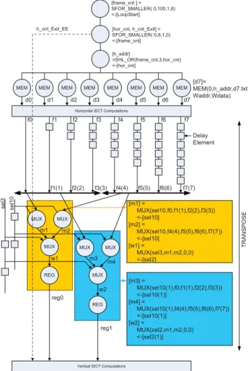
B. 2-D-IDCT Algorithm
We used a fixed point model of the algorithm [24]. The algorithm is composed of three parts: horizontal pass, trans-position, and vertical pass. In the horizontal pass, the rows of the 8× 8 matrix are read and the eight-point 1-D IDCT of the row is computed. Since there are eight rows in the matrix, this operation is repeated 8 times. The transposition phase of the algorithm transposes the resulting matrix obtained from the horizontal pass. In the final phase, the matrix is read again row-wise and the 1-D IDCT of each row is computed. The challenging part of the algorithm is the transposition phase.
Fig. 11 illustrates the CDFG and LRC of the algorithm. This algorithm computes 2-D-IDCT of 100 frames, where a frame is composed of 64 words. The code assumes that the input data is stored in eight arrays. While the input arrays are being filled, the IDCT computation can run concurrently. Hence, the time to get data to the memory can be hidden. The two SFOR_SMALLER instructions at the beginning of the code are used for frame counting and horizontal line
Fig. 10. LRC code and CDFG of maximum value of an array.
Fig. 11. LRC code and CDFG of 2-D-IDCT algorithm.
counting, respectively. The SHR_OR instruction computes the address, which is used to read data from the eight memory locations. MUX (multiplex) instructions in the code are used for transposition. The MUX instruction has five operands: the first operand is used as the selection input, and the remaining four operands are to be multiplexed. In order to multiplex eight operands, three multiplexers are used. The variables
[f0, f1, …, f7] are the results of the horizontal IDCT. These variables are used as the input operands of the multiplexers. f0 is connected to the input of the multiplexer directly, whereas f1 is delayed one clock cycle; hence f1(1) and f2 are delayed two cycles. The horizontal results are queued in a pipeline for the first register, reg0. For the second register, reg1, sel10, and sel3, which are selection operands of the multiplexers, are delayed, so that the second horizontal results are queued. The transposition operation is performed by using 24 MUX instructions and 31 delay elements.
The IID parameter of the SFOR_SMALLER instruction for horizontal line counting is set to 0. Therefore, an index is generated every clock cycle, and computation of eight horizontal IDCTs takes eight clock cycles. The computation of the vertical IDCTs takes eight clock cycles as well. The computations of horizontal and vertical IDCTs are pipelined. Thus, a 2-D-IDCT is computed in nine clock cycles on the average (one clock cycle is lost in loop instructions). The computation of 100 frames takes only 930 clock cycles.
C. UMTS Turbo Decoder
Turbo codes [25] are widely used in telecommunications standards as in UMTS [26] for forward error correction.
A Turbo decoder requires an iterative decoding algorithm in which two soft-in-soft-output (SISO) decoders exchange information. The first SISO corresponds to the convolutional encoder that encodes the data in the normal order, and the second one corresponds to the encoder that encodes the data in an interleaved order. The operations performed in these two decoders are the same. Therefore, only a single decoder, which serves as both the first SISO and the second SISO sequentially, is implemented in LRC. Inside a SISO decoder, a forward recursion is performed first. At each step, the probabilities of states are stored in memories and then a backward recursion is performed. During the backward recursion, the probabilities of states computed in forward recursion and the current backward state probabilities are used to compute a new likelihood ratio for the symbol to be decoded [27].
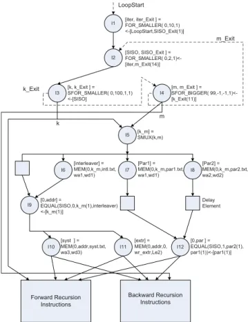
Fig. 12 illustrates the CDFG and LRC of a Turbo decoder. The first loop instruction (I1) is used to count the iterations, which start from 0 and end at 9. The second loop (I2) counts SISOs. When SISO is 0, the instructions inside the loop body correspond to the first SISO in the algorithm. When it is 1, it behaves as the second SISO. The third loop (I3), k is used for forward recursion, and the loop (I4), m is used for backward recursion. The forward recursion and backward recursion instructions read the input data from the same memory. Hence, k and m are multiplexed with the SMUX instruction. k and m cannot be active at the same time, since the loop for m starts after the loop for k exits. The input likelihoods are stored in three arrays, syst, par1, and par2 corresponding to the systematic, the parity of first encoder, and the parity of second encoder, respectively. extr is for the extrinsic information memory. The first SISO uses par1 as the parity likelihood, and the second SISO uses par2. The EQUAL instruction (I12) corresponding to par selects either par1 or par2 depending on the value of SISO. The arrays for
Fig. 12. LRC code and CDFG of UMTS turbo decoder.
syst and extr must be accessed in the normal order for the first SISO and in the interleaved order for the second SISO. The read address of the memory, inter_index, is set to k_m(2) when SISO is 0 and interleaver when SISO is 1 by using an EQUAL instruction (I9), where interleaver is the interleaved address that is read from a memory.
VI. RESULTS
A. Physical Implementation
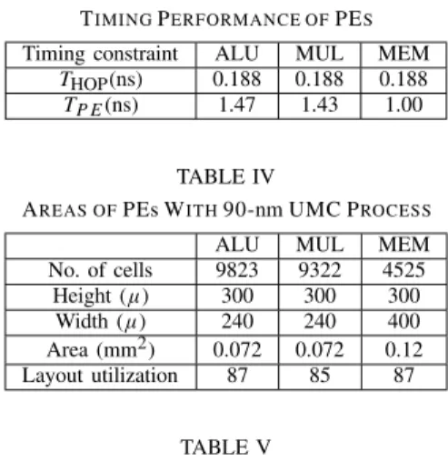
We utilized Cadence RTL Compiler for logical synthesis and Cadence Encounter for layout generation. Faraday library6 for 90-nm UMC CMOS process technology was used for standard cells. Behavioral and gate-level simulations were performed on Cadence NC-VHDL and NC-Verilog. The steps taken in physical implementation were similar to standard ASIC implementation steps. Since BilRC has a program-mable segmented-interconnect architecture, it is not possible to directly synthesize the top-level BilRC HDL code. The Cadence synthesis tool can find and optimize the critical path. Since the configuration for BilRC is unknown to the tool, it can not determine the critical path. Therefore, PEs are synthesized individually by applying two timing constraints. The combinational path delay constraint (THOP) is applied in order to determine the time delay to traverse a PE. The clock constraint is applied in order to determine the path between any PE input and the register output of the PC. The plain clock constraint is used to determine the longest delay path
between two registers. Since the input of PE is not registered, this condition is specified to the tool with input switch [28]. Table III shows the timing results achieved at +25 °C.
Table IV shows the silicon area for PEs. The area of a PE contains both the area of the PC and the area of the PRBs. The area of the PRBs is about 0.03 mm2. 42% of the PE area is used for PRBs in ALU and MUL and 25% for MEM. PEs were first synthesized with the Cadence RTL compiler and then placed and routed with the Cadence Encounter tool. The last row in Table IV shows the percentage utilization of the rectangular area of the layout. The heights of PEs are chosen to be the same value: 300µm. However, the widths are variable. Since PEs can be connected by abutment to neighboring PEs, no further area is required for interconnections. The area value for MEM contains both the area of the logic cells and the area of SRAM.
B. Comparison to TI C64+ DSP
Table V depicts the cycle count performance of all algo-rithms mapped to BilRC. The area results and the utilization of the PEs are shown in Table VI. The achieved clock frequencies for the applications are listed in Table VII. When mapping applications to BilRC, the minimum rectangular area containing a sufficient number of PEs is selected. Table V shows the cycle count performance of the applications mapped on BilRC and a TI C64+ 8 issue VLIW processor. BilRC always outperforms TI C64+ DSP. The improvements are due to adjustable parallelism in BilRC, whereas in TI C64+ the maximum number of instructions that can be executed in a single clock cycle is limited. For example, the UMTS Turbo decoder and 2-D-IDCT implementations on BilRC have average instruction per cycle (IPC) values of about 30 and 128, respectively [3]. For TIs eight-issue VLIW processor, the maximum IPC is eight.
Further improvements are possible. For example, the perfor-mance of the maxval and dotprod algorithms can be doubled by storing the arrays in 16 memory blocks and processing accordingly. The performances for the TI C64+ implementa-tions are obtained by coding these algorithms in the assembly language. Obtaining these performances is quite difficult and requires considerable expertise in the specific assembly language for the targeted VLIW processor. Tables VI and VII show the area and timing results for BilRC. Although, TMS320C64 has a faster clock of 1000 MHz, BilRC provides better throughput results (except for the maxval and dotprod algorithms). The TMS320C64’s processor core area is reported to be 2 mm2 [15], while the whole chip area, including two level caches and peripherals, is 20 mm2. As is clear from Table VIII, all of the applications mapped on BilRC requires an area of less than 20 mm2(except the FIR Complex algorithm). If the primary concern in regard to implementing an application is the area, the parallelism degree can be decreased to fit the given area. For example, the area of the FIR Complex can be reduced to a quarter of the value indicated by performing complex multiplication operations in the algorithm sequentially. BilRC, and its computation model, allow the designer to balance the area and performance.
TABLE III
TIMINGPERFORMANCE OFPES
Timing constraint ALU MUL MEM
THOP(ns) 0.188 0.188 0.188
TP E(ns) 1.47 1.43 1.00
TABLE IV
AREAS OFPEs WITH90-nm UMC PROCESS
ALU MUL MEM
No. of cells 9823 9322 4525 Height (µ) 300 300 300 Width (µ) 240 240 400 Area (mm2) 0.072 0.072 0.12 Layout utilization 87 85 87 TABLE V
CYCLECOUNTPERFORMANCE OFBENCHMARKS
Application Notes BilRC cycle count TI C64+ cycle count Ratio 2-D-IDCT 100 frames [24] 931 9262 9.95
maxval Array size [24] 128 22 42 1.91
dotprod Dot product, arrayssize 256 [24] 41 79 1.93
maxidx Index of maximum,
array size 128 [24] 22 82 3.73 FIR 32-tap FIR filter, datasize 256 [24] 266 2065 8.07
vecsum Vector addition, size
256 [24] 36 106 2.94
FIR complex
16-tap complex FIR filter, data size
256 [24] 266 4112 15.5 16-state viterbi Information of size 100 513 NA NA 8-state turbo Section V-C 8590 NA NA FFT Radix-2, 1024 point 10 351 NA NA Multirate FIR
Rate 2, 16-tap FIR
filter 1032 NA NA
Multichannel FIR
2 channel 16-tap FIR
filter 2057 NA NA
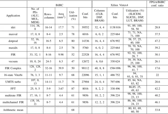
C. Comparison to Xilinx Virtex-4 FPGA
One of the main advantages of CGRA as compared to FPGAs is the reduction in the configuration size. This reduc-tion allows CGRA to be configured at run time. For a compar-ison of configuration size, Xilinx Virtex4 FPGA is used. This FPGA is partitioned into four rows. Inside a row, 16 config-urable logic blocks (CLB) form a column. Similarly, there are four BRAMs and eight DSP48 blocks in a column. The resources forming a column are configured together. Table IX shows the number of frames required to configure different column types [29]. A configuration frame is composed of 1312 bits. For CLB and DSP48 (the multiplier block), the configuration stream configures both the functionality of the blocks in the column and the interconnection network. The configuration stream for BRAM initialization and interconnect is separately provided [29].
To make a fair configuration size comparison, only the required number of configuration columns should be taken into account. This is done by using the Xilinx PlanAhead tool, which allows all resources (CLB, DSP48, BRAM) to be placed
TABLE VI
COMPARISON OFCONFIGURATIONSIZES OFBILRCANDXILINXVIRTEX4
BilRC Xilinx Virtex4
FPGA/BilRC conf. ratio Application No. of PEs (ALU, MUL, MEM) Rows-columns Area (mm2) Util-ization (%) Conf. bits Columns (CLB, DSP, BRAM) Conf. bits Utilization (%) (SLICEM, SLICEL, DSP, LUT, BRAM) idct 114, 38, 8 16-14 17.7 71 39552 32, 4, 4 1138 816 91, 89, 100, 58, 50 28.8 maxval 17, 0, 8 8-4 2.5 78 6016 6, 0, 2 225 664 71, 71, NA, 71, 100 37.5 dotprod 32, 16, 16 16-5 6.5 80 14336 16, 4, 4 676 992 58, 57, 25, 40, 100 47.2 maxidx 17, 0, 8 8-4 2.5 78 5760 6, 0, 2 225 664 70, 70, NA, 70, 100 39.2 FIR 33, 32, 1 8-16 9.98 52 22528 16, 4, 4 676 992 92, 92, 100, 28, 7 30.1 vecsum 10, 0, 24 24-3 6.3 47 12672 6, 0,6 330 624 39, 39, NA, 25, 100 26.1 FIR Complex 128, 128, 2 32-16 39.9 50 90112 40, 8, 8 1584 896 96, 96, 100, 41, 7 17.6 16-state Viterbi 76, 3, 3 11-11 9.7 68 22096 15, 1, 1 486 752 94, 93, 0, 93, 75 22 UMTS turbo 107, 0, 13 14-11 11.7 78 27904 24, 0, 4 797 696 85, 84, NA, 83, 82 28.6 FFT 25, 9, 5 5-9 3.67 87 8016 8, 2, 2 338 496 86,85, 25, 49, 63 42.2 multirate FIR 17, 16, 1 8-7 4.4 61 9856 10, 2, 2 396 224 98, 98, 100, 23, 13 40.2 multichannel FIR (18, 16, 2) 8-7 4.4 61 9856 12, 2, 2 396 224 86, 86, 100, 24, 23 46.1 Arithmetic mean 68 80, 81, 69, 60, 50 33.8
and routed within a partition block (PBlock). When drawing a PBlock, the height must be at a row boundary since the resources in a column are configured together. The width of the PBlock, on the other hand, must be selected so that enough resources exist in the PBlock.
HDL code generated from the LRC-HDL converter is used as the input to the Xilinx ISE tool. When mapping the applications to the FPGA, the locations of the PBlocks are manually selected to increase the utilization of resources to reduce configuration size. When mapping the applications to BilRC, a minimum-sized rectangle, starting from the top-left PE, is formed containing sufficient resources (ALU, MEM, MUL). The BilRC placement and routing tool places PEs in the selected rectangle. Only the interconnect resources within the selected rectangle area are used for signal routing. The tool is forced to use only three ports per PE side (Np = 3), and
all applications are routed without congestion. Although three ports are enough for the selected applications, all performance results (configuration size, area, and timing) are given for
Np = 4, leaving extra flexibility for more complex
applica-tions. The results are summarized in Table VI. For example, the FFT algorithm requires 39 PEs arranged in nine rows and five columns with an utilization ratio of 87% and it can be configured with just 8016 bits.7 To implement the same algorithm, Virtex4 requires eight CLBs, two DSP, and two BRAM columns configured with 338 496 bits. Utilizations
7This number includes the configuration bits for unused PEs.
of various logic resources are shown in the ninth column of the table. The last column lists the improvements in the configuration size varying from 17.6× to 47.2×.
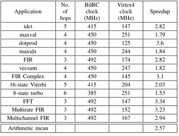
CGRAs are expected to provide better timing performance as compared to FPGAs. The arithmetic units of a CGRA are pre-placed and routed, whereas in an FPGA, these units are formed from look-up-tables (LUTs). The critical path for an instruction in a CGRA is formed from gates that are, in general, faster than LUTs. In [30] the gap between FPGA and ASIC implementations is measured, it is found that ASICs are on the average three times faster than FPGA implementations. This value is found by allowing the use of the hard blocks (multiplier and memory) during algorithm mapping to an FPGA. Since CGRAs cannot be faster than ASICs, a well-designed CGRA is at best three times faster than an FPGA. Table VII shows the critical path delays of BilRC and Xilinx Virtex4 implemented with the same 90-nm CMOS technology. The second column shows the worst case hop count between a source PE and a destination PE. The critical path of PEs is taken as 1.47 ns, which is the worst performance among PEs. Improvements in the range of 1.53× and 3.6× are obtained.
D. Comparison to Other CGRAs
The 2-D-IDCT algorithm has been implemented on many CGRAs. The results are shown in Table VIII. In terms of cycle count, BilRC is 3.2 times faster than the fastest CGRA, ADRES [15]. In terms of throughput, BilRC is 2.2 times
TABLE VII
CRITICALPATHCOMPARISONOFBILRCANDFPGA
Application No. of hops BilRC clock (MHz) Virtex4 clock (MHz) Speedup idct 5 415 147 2.82 maxval 4 450 251 1.79 dotprod 4 450 125 3.6 maxidx 4 450 244 1.84 FIR 3 492 174 2.82 vecsum 4 450 247 1.82 FIR Complex 4 450 145 3.1 16-state Viterbi 5 415 204 2.03 8-state turbo 6 385 251 1.53 FFT 3 492 147 3.34 Multirate FIR 3 492 152 3.23 Multichannel FIR 3 492 167 2.94 Arithmetic mean 2.57 TABLE VIII
AREA, TIMING,ANDCYCLECOUNTRESULTS FOR THE
2-D-IDCT ALGORITHM CGRA No. of PEs Area (mm2) Granu-larity Average cycle ount Clock freq. (MHz) Throughput (million IDCT/sec) BilRC 152 11.90 16-bit 9.3 415 44.6 ADRES 64 4 32-bit 30 600 20 MORA 22 1.749 8-bit 108 1000 10.2 MorphoSys 64 11.11 16-bit 37 NA NA TABLE IX
CONFIGURATIONFRAMES FORFPGA RESOURCES
Column type CLB BRAM interconnect
BRAM
content DSP48 No. of
frames 22 20 64 21
faster than ADRES. The maximum clock frequency of BilRC for IDCT algorithm is found to be 415 MHz. ADRES and MORA work at a constant frequency of 600 and 1000 MHz, respectively. The timing result of MorphoSys is not available for 90-nm technology, and its area result is scaled to 90 nm in the table. The lower operating frequency of BilRC is due to its segmented interconnect network. BilRC uses a larger silicon area for implementing the IDCT algorithm, mainly due to its flexible segmented interconnect architecture which is crucial for the high performance implementation of a broad range of applications. The area result for MorphoSys includes the area for a small RISC processor and some other peripherals. It was reported that more than 80% of the whole chip area was used for the reconfigurable arrays [31]. The area result for ADRES includes the area of the VLIW processor as well.
BilRC does not require an external processor for loop control or execution control; however, an external processor can be attached to BilRC for the execution of sequential code for initializations and parameter loading.
The ADRES processor is a mature CGRA. ADRES has the significant advantage of mapping full applications from the C language, a property that BilRC does not yet have.
TABLE X IPCANDSD COMPARISON
FFT IDCT IPC SD IPC SD BilRC 17.8 54% 128 85% ADRES [11] 23.3 37% 31(V), 42(H) 45%(V), 47%(H) ADRES [32] 10.4 65% NA NA ADRES [33] 12.4 78% 13.3 83%
In BilRC, PEs are statically configured, whereas the reported CGRAs rely on dynamic reconfiguration. In general, dynamically reconfigurable CGRAs are expected to provide better PE utilization. However, due to its execution-triggered computation model and flexible interconnect architecture, BilRC provides better or comparable PE utilization. For example, BilRC requires 152 PEs for the IDCT algorithm with an average IPC of about 128 [3]. Therefore, the scheduling density (SD) is about 85%, whereas ADRES [11] has SD of 45% for the vertical phase of IDCT (V) and 66% for the horizontal phase of IDCT (H). Table X compares BilRC with three ADRES implementations.
VII. CONCLUSION
We have presented BilRC and its LRC language, capable of implementing state-of-the-art algorithms with very good performance in speed, area utilization, and configuration size. BilRC contains three different kinds of PEs. Using 90-nm technology, 14 16-bit PEs can fit into 1 mm2of silicon. The total number of PEs is equal to the number of instructions in LRC code. The FFT algorithm can be implemented with just 39 instructions.
The reduction in configuration size is possible mainly for two reasons. First, 17-bit signals were routed together in BilRC, whereas in an FPGA each bit was individually routed. Second, the functionality of a PE was selected with an eight-bit opcode, whereas in an FPGA functionality was programmed by filling in several LUTs. The configuration size, area, and timing performance can be further improved by optimizing the interconnect architecture.
BilRC can be used as an accelerator attached to a DSP processor for applications requiring high computation power. Due to the run-time configurability of BilRC, several applica-tions can be run in a time-multiplexed manner. BilRC may also be used as an alternative to FPGAs, especially for applications having word level granularity. Almost all telecommunications and signal processing algorithms have word-level granularity. The main advantages of BilRC as compared to FPGAs are run-time configurability due to reduced configuration size, reduced compilation time, and faster frequency of operation.
REFERENCES
[1] T. Vogt and N. Wehn, “A reconfigurable ASIP for convolutional and turbo decoding in an SDR environment,” IEEE Trans. Very Large Scale
Integr. (VLSI) Syst., vol. 16, no. 10, pp. 1309–1320, Oct. 2008.
[2] O. Muller, A. Baghdadi, and M. Jezequel, “From parallelism levels to a multi-ASIP architecture for turbo decoding,” IEEE Trans. Very Large
[3] O. Atak and A. Atalar, “An efficient computation model for coarse grained reconfigurable architectures and its applications to a reconfig-urable computer,” in Proc. 21st IEEE Int. Conf. Appl.-Specific Syst. Arch.
Process., Jul. 2010, pp. 289–292.
[4] R. Hartenstein, “A decade of reconfigurable computing: A visionary retrospective,” in Proc. Eur. Design, Autom. Test Conf., 2001, pp. 642–649.
[5] B. De Sutter, P. Raghavan, and A. Lambrechts, “Coarse-grained reconfig-urable array architectures,” in Handbook of Signal Processing Systems, S. S. Bhattacharyya, E. F. Deprettere, R. Leupers, and J. Takala, Eds. New York: Springer-Verlag, 2010, pp. 449–484.
[6] K. Compton and S. Hauck, “Reconfigurable computing: A survey of systems and software,” ACM Comput. Surv., vol. 34, no. 2, pp. 171–210, 2002.
[7] Y. Kim and R. Mahapatra, “Dynamic context compression for low-power coarse-grained reconfigurable architecture,” IEEE Trans. Very Large
Scale Integr. (VLSI) Syst., vol. 18, no. 1, pp. 15–28, Jan. 2010.
[8] S. C. Goldstein, H. Schmit, M. Budiu, S. Cadambi, M. Moe, and R. R. Taylor, “PipeRench: A reconfigurable architecture and compiler,” IEEE
Comput., vol. 33, no. 4, pp. 70–77, Apr. 2000.
[9] C. Ebeling, C. Fisher, G. Xing, M. Shen, and H. Liu, “Implementing an OFDM receiver on the RaPiD reconfigurable architecture,” IEEE Trans.
Comput., vol. 53, no. 11, pp. 1436–1448, Nov. 2004.
[10] C. Ebeling, D. Cronquist, and P. Franklin, “RaPiD - reconfigurable pipelined datapath,” in Field-Programmable Logic Smart Applications,
New Paradigms and Compilers (Lecture Notes in Computer Science),
R. Hartenstein and M. Glesner, Eds. Berlin, Germany: Springer-Verlag, 1996.
[11] B. Mei, S. Vernalde, D. Verkest, H. De Man, and R. Lauwereins, “Exploiting loop-level parallelism on coarse-grained reconfigurable architectures using modulo scheduling,” IEE Proc. Comput. Digital
Tech., vol. 150, no. 5, pp. 255–61, Sep. 2003.
[12] B. Mei, S. Vernalde, D. Verkest, H. De Man, and R. Lauwereins, “ADRES: An architecture with tightly coupled VLIW processor and coarse-grained reconfigurable matrix,” in Field Programmable Logic
and Application (Lecture Notes in Computer Science), vol. 2778,
P. Y. K. Cheung and G. Constantinides, Eds. Berlin, Germany: Springer-Verlag, 2003, pp. 61–70.
[13] B. Mei, A. Lambrechts, J.-Y. Mignolet, D. Verkest, and R. Lauwereins, “Architecture exploration for a reconfigurable architecture template,”
IEEE Design Test Comput., vol. 22, no. 2, pp. 90–101, Mar.–Apr. 2005.
[14] F. Bouwens, M. Berekovic, A. Kanstein, and G. Gaydadjiev, “Architec-tural exploration of the ADRES coarse-grained reconfigurable array,” in Reconfigurable Computing: Architectures, Tools and Applications (Lecture Notes in Computer Science), P. Diniz, E. Marques, K. Bertels, M. Fernandes, and J. Cardoso, Eds. Berlin, Germany: Springer-Verlag, 2007.
[15] M. Berekovic, A. Kanstein, B. Mei, and B. De Sutter, “Mapping of nomadic multimedia applications on the ADRES reconfigurable array processor,” Microprocess. Microsyst., vol. 33, no. 4, pp. 290–294, Jun. 2009.
[16] H. Singh, M.-H. Lee, G. Lu, F. Kurdahi, N. Bagherzadeh, and E. C. Filho, “MorphoSys: An integrated reconfigurable system for data-parallel and computation-intensive applications,” IEEE Trans.
Comput., vol. 49, no. 5, pp. 465–481, May 2000.
[17] M. Lanuzza, S. Perri, P. Corsonello, and M. Margala, “Energy effi-cient coarse-grain reconfigurable array for accelerating digital signal processing,” in Integrated Circuit and System Design. Power and
Timing Modeling, Optimization and Simulation (Lecture Notes in
Computer Science), L. Svensson and J. Monteiro, Eds. Berlin, Germany: Springer-Verlag, 2009.
[18] W. Vanderbauwhede, M. Margala, S. Chalamalasetti, and S. Purohit, “Programming model and low-level language for a coarse-grained reconfigurable multimedia processor,” in Proc. Int. Conf. Eng. Reconfig.
Syst. Algorithms, Las Vegas, NV, Jul. 2009, pp. 1–7.
[19] A. H. Veen, “Dataflow machine architecture,” ACM Comput. Surv., vol. 18, pp. 365–396, Dec. 1986.
[20] C. Jang, J. Kim, J. Lee, H.-S. Kim, D.-H. Yoo, S. Kim, H.-S. Kim, and S. Ryu, “An instruction-scheduling-aware data partitioning technique for coarse-grained reconfigurable architectures,” in Proc.
SIGPLAN/SIGBED Conf. Lang., Compil. Tools Embedded Syst., 2011,
pp. 151–160.
[21] B. De Sutter, O. Allam, P. Raghavan, R. Vandebriel, H. Cappelle, T. V. Aa, and B. Mei, “An efficient memory organization for high-ILP inner modem baseband SDR processors,” J. Signal Process. Syst., vol. 61, no. 2, pp. 157–179, Nov. 2010.
[22] V. Betz and J. Rose, “VPR: A new packing, placement and routing tool for fpga research,” in Field-Programmable Logic and
Applica-tions (Lecture Notes in Computer Science), W. Luk, P. Cheung, and
M. Glesner, Eds. Berlin, Germany: Springer-Verlag, 1997.
[23] L. McMurchie and C. Ebeling, “PathFinder: A negotiation-based performance-driven router for FPGAs,” in Proc. 3rd Int. ACM Symp.
Field-Program. Gate Arrays, 1995, pp. 111–117.
[24] Texas Instruments Inc. (2010, Jan.). TMS320C674x Low Power DSPs, Dallas, TX [Online]. Available: http://focus.ti.com/en/download/dsp/ c64plusbmarksasmfiles.zip
[25] C. Berrou, A. Glavieux, and P. Thitimajshima, “Near Shannon limit error-correcting coding and decoding: Turbo-codes. 1,” in Proc. Int.
Conf. Commun., Geneva, Switzerland, 1993, pp. 1064–1070.
[26] European Telecommunications Standards Institute, Universal Mobile
Telecommunications System (UMTS): Multiplexing and Channel Coding (FDD), TS Standard 125.212, 2000.
[27] M. C. Valenti and J. Sun, “The UMTS turbo code and an efficient decoder implementation suitable for software-defined radios,” Int. J.
Wireless Inf. Netw., vol. 8, no. 4, pp. 203–215, 2001.
[28] Synopsys Timing Constraints and Optimization User Guide Version
C-2009.06. (2009, Jun.) [Online]. Available: http://acms.ucsd.edu/_files/
tcoug.pdf
[29] C. Carmichael and C. W. Tseng. Correcting Single-Event Upsets
in Virtex-4 Platform FPGA Configuration Memory. (2011, Apr.)
[Online]. Available: http://www.xilinx.com/support/documentation/ application_notes/xapp1088.pdf
[30] I. Kuon and J. Rose, “Measuring the gap between FPGAs and ASICs,”
IEEE Trans. Comput.-Aided Design Integr. Circuits Syst., vol. 26, no. 2,
pp. 203–215, Feb. 2007.
[31] M.-H. Lee, H. Singh, G. Lu, N. Bagherzadeh, F. J. Kurdahi, E. M. Filho, and V. C. Alves, “Design and implementation of the MorphoSys reconfigurable computing processor,” J. VLSI Signal Process., vol. 24, nos. 2–3, pp. 147–164, Mar. 2000.
[32] B. Bougard, B. De Sutter, S. Rabou, D. Novo, O. Allam, S. Dupont, and L. Van der Perre, “A coarse-grained array based baseband processor for 100 Mb/s+ software defined radio,” in Proc. Conf. Design, Autom.
Test Eur., 2008, pp. 716–721.
[33] B. De Sutter, P. Coene, T. Vander Aa, and B. Mei, “Placement-and-routing-based register allocation for coarse-grained reconfigurable arrays,” in Proc. ACM SIGPLAN-SIGBED Conf. Lang.,
Compil., Tools Embedded Syst., 2008, pp. 151–160.
Oguzhan Atak received the B.S. degree from Eskisehir Osmangazi University, Eskisehir, Turkey, in 2002, and the M.S. degree from Bilkent Univer-sity, Ankara, Turkey, in 2006, both in electrical engi-neering, where he is currently pursuing the Ph.D. degree in electrical engineering.
He was a Visiting Researcher with RWTH, Aachen, Germany, in 2005. His current research interests include application-specific instruction set processors, field programmable gate arrays, and coarse-grained reconfigurable architectures.
Abdullah Atalar (M’88–SM’90–F’07) received the B.S. degree from Middle East Technical University, Ankara, Turkey, in 1974, and the M.S. and Ph.D. degrees from Stanford University, Stanford, CA, in 1976 and 1978, respectively, all in electrical engi-neering.
He was with Hewlett Packard Laboratory, Palo Alto, CA, in 1979. From 1980 to 1986, he was an Assistant Professor with Middle East Technical University. In 1986, he joined Bilkent University, Ankara, as the Chairman of the Electrical and Elec-tronics Engineering Department and was involved in the founding of the Department, where he is currently a Professor. In 1995, he was a Visiting Professor with Stanford University. From 1996 to 2010, he was the Provost of Bilkent University. He is currently the Rector with the same university. His current research interests include micromachined devices and microwave electronics.