Digital Fourier optics
Haldun M. Ozaktas and David A. B. Miller
Analog Fourier optical processing systems can perform important classes of signal processing operations in parallel, but suffer from limited accuracy. Digital–optical equivalents of such systems could be built that share many features of the analog systems while allowing greater accuracy. We show that the digital equivalent of any system consisting of an arbitrary number of lenses, filters, spatial light modulators, and sections of free space can be constructed. There are many possible applications for such systems as well as many alternative technologies for constructing them; this paper stresses the potential of free-space interconnected active-device-plane-based optoelectronic architectures as a digital signal processing environment. Implementation of the active-device planes through hybridization of optoelectronic components with silicon electronics should allow the realization of systems whose performance exceeds that of purely electronic systems. r1996 Optical Society of America
1. Introduction
The term Fourier optics is used in several different ways. Sometimes it is used to refer to the theory of centered optical systems based on the Fresnel ap-proximation and the assumption of thin lenses and transmissive elements. The ease with which the Fourier transform and various signal processing operations can be realized with these systems has led to the term’s also being used almost synony-mously with optical information processing or opti-cal signal processing.1,2 These systems can exhibit
space–bandwidth products that exceed 106 without
excessive difficulty, a capacity that can be almost fully utilized in realizing space-invariant 1convolu-tion-type2 operations and less efficiently for space-variant operations.3–5 These operations are
real-ized in the time it takes light to propagate through the system, so that the overall system speed is often limited only by the intrinsic delay Tdof the input– output devices. What is most noteworthy about these systems is the way in which a large number of parallel channels undergo several consecutive opera-tions in pipeline fashion, with opportunity for global percolation of information at every stage of the pipeline. Despite these advantages, such analog–
optical information processing systems suffer from certain serious disadvantages, common to most ana-log systems. In particular, the dynamic range in amplitude seems to be limited to ,2 orders of magnitude, disallowing signal processing operations that require greater accuracy or the concatenation of many stages to be performed.
Recently there has been significant progress in making so-called smart pixels: two-dimensional 12-D2 arrays of electronic processing units, each with optical inputs and outputs.6 Such smart pixels
have the potential to capitalize on the advanced state of certain electronics technologies together with the advantages of optics as an interconnection medium.7 One significant challenge with such
elec-tronic arrays is to devise concepts and architectures that provide a platform for realizing this potential.
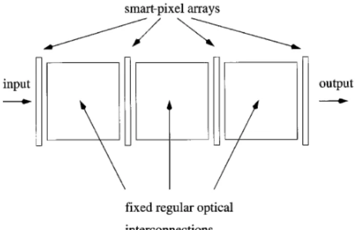
In this paper we show that the basic architectural concepts of analog Fourier optics allow the specifica-tion of just such a platform, which enables the construction of a broad range of interesting digital signal processing1DSP2 systems. It is important to emphasize that we are not proposing merely to insert smart-pixel arrays in existing Fourier optical systems. Rather, we show that the digital optical equivalent of any analog Fourier optical system consisting of lenses, sections of free space, passive or active transmissive elements, etc., can be con-structed with properly chosen1or programmed2 smart-pixel arrays interconnected in succession with fixed and regular connection patterns. Figure 1 schemati-cally depicts the general class of systems being considered. The construction of such systems has already been demonstrated and investigated for
H. M. Ozaktas is with the Department of Electrical Engineer-ing, Bilkent University, 06533 Bilkent, Ankara, Turkey. D. A. B. Miller is with AT&T Bell Laboratories, 101 Crawfords Corner Road, Holmdel, New Jersey 07733.
Received 3 July 1995; revised manuscript received 27 October 1995.
0003-6935@96@081212-08$06.00@0
applications such as telecommunications switching fabrics8and image processing.9
In an analog–optical processing system, each num-ber is represented by the amplitude or the intensity of light at a certain point at a given time. In the digital–optical systems discussed here, each complex number is represented by a binary string. Physi-cally, this binary string will usually be represented bit serially by the on–off modulated intensity of a light beam 1or possibly differential pairs of light beams2. 1Of course, we could also choose to use a group of parallel light beams to represent the binary digits in parallel, but this is not likely because, given the present technological constraints of smart-pixel technologies, we are more likely to run at high bit rates with a moderate number of beams that at low bit rates with a large number of beams.2 In analog systems, it is possible to perform many interesting operations by using simple lenses and transparencies. Digital systems require more sophisticated optics for mapping 2-D arrays of distinct light beams accord-ing to certain discrete regular connection patterns 1such as the Banyan or perfect shuffle2 between discrete optical input–output pixels on consecutive processing planes. The benefits of digital–optical systems with respect to analog–optical systems are unlimited accuracy and cascadability and much greater flexibility in implementing different kinds of functions and algorithms, including those that in-volve nonlinear operations and operations that re-quire memory. The major benefit with respect to purely electronic systems is the ability to implement high-speed, high-density global interconnections in three dimensions with less overall power dissipa-tion.
2. Digital Equivalents of Analog Components and Operations
We now discuss digital equivalents of common anal-og–optical operations and components.
We first describe the equivalent of a dynamically programmable thin transmissive element, better known as a spatial light modulator1SLM2. Such an element can be realized by using many of the several
so-called smart-pixel technologies; we assume use of the hybrid self-electro-optic-effect-device1SEED2 tech-nology that we find particularly promising.10 In
this technology, quantum-well diodes, which are capable of acting as high-speed optical detectors1for input2 and optical modulators 1for output2, are bonded to silicon integrated circuits. For the purpose of this paper, it is sufficient to note that this is essen-tially a technology that allows optical input and output from a mainstream silicon VLSI circuit. Current technology requires optical inputs or out-puts to be spaced by approximately tens of microme-ters or more apart. If these optical inputs and outputs are arranged in the form of a regular array of pixels, we essentially obtain a pixelated SLM with plenty of silicon circuit area per pixel. In operation, optical bit streams representing quantized numbers are detected and read in by each pixel. The cir-cuitry corresponding to each pixel modifies this number according to purpose. Then the modified number is reconverted into an optical bit stream. Note that nonlinear operations as well as operations with memory are possible. The flexibility and the programmability of these devices far exceed those of their analog counterparts. Hence, in addition to allowing improved accuracy, the digital approach will allow certain operations that are inherently difficult or impossible with analog systems, such as buffering, consecutive frame differencing, etc.
A thin spherical lens is simply a special case of a thin transmissive element. Thus its digital equiva-lent may be realized by the use of a hardwired version of the SLM’s discussed in the paragraph above. 1If desired, a programmable SLM would allow us to realize a lens with adjustable focal length, pupil size, etc.2 The complex numbers repre-senting the amplitude of light at each pixel will simply be multiplied by the appropriate phase fac-tors characteristic of a lens. 1In contrast with a real lens, this one will have no aberrations, but it will of course exhibit quantization error.2 There is no di-rect analog of free-space propagation, although we see below that it is possible to simulate free-space propagation. In any case, it is important to note that lenses and free-space propagation are not ends but means. They are the basic building blocks of analog Fourier optics systems, but need not necessar-ily be the basic building blocks of digital Fourier optics systems. It is more useful to look at the classes of operations performed by analog optical systems at a higher level and to understand how to perform these operations with digital–optical sys-tems, rather than to try to imitate analog systems at the lowest level.
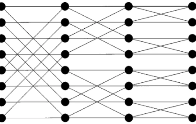
One of the most important operations in signal processing is the Fourier transform. The digital
Œ
N 3Œ
N point 2-D discrete Fourier transform1DFT2 can be realized by the use of an ,log2 N-stage 2-DBanyan network.11 1Figure 2 shows a
one-dimen-sional11-D2 Banyan, which is easier to comprehend. The 2-D DFT can also be realized in two steps
Fig. 1. Schematic depiction of the general class of digital–optical systems discussed.
involving only 1-D transforms, performed in parallel.2 Given the basic similarity of this type of network with some of the switching fabrics demonstrated in Ref. 8 and the emerging yields and processing power of hybrid SEED’s, we infer that a 16 3 16 DFT could likely be realized with technology being demon-strated now1as we discuss below2.
Of course, by combining two Fourier-transform stages with a SLM in between, we obtain the ability to realize convolutions and correlations by frequency-domain filtering 1these are also among the most important operations in signal processing2. The flexibility of the digital approach will also allow most other unitary image transforms12 to be realized as
well, with similar log2N-stage architectures.
Be-cause such transforms are used in applications such as transform-domain image compression, it should be possible to contemplate digital–optical architec-tures for this and similar purposes. The three-dimensional data flow possible with optics should allow one to surpass the performance of fully elec-tronic approaches. Analog–optical approaches would, in most cases, not be able to offer sufficient dynamic range for this type of application.
3. Performance Comparison with Electronic Systems We can give some estimates of the capabilities of such digital–optoelectronic processing systems and compare them with purely electronic systems. Let us consider the task of computing an N 5 16 3 16 point 2-D DFT. 1This is comparable with the task of computing an N 5 256 point 1-D DFT.2
The optoelectronic system will consist of log2 N
silicon device planes with optoelectronic inputs– outputs1smart-pixel arrays2 of the kind described in Ref. 10, interconnected according to the butterfly 1Banyan2 pattern 1or equivalent2. There are many ways of designing such a system. Here we consider one example in its broad outlines, omitting most details.
Let us first concentrate on one of the silicon device planes. A complex multiplier is the dominant part of a radix-2 butterfly element used in Fourier-transform processors. For example, the use of a standard serial–parallel complex multiplication
ar-chitecture with a transistor count, as enumerated by Smith and Denyer,13would require 9208 transistors
in a complementary metal-oxide semiconductor 1CMOS2 for multiplying two complex numbers with 16-bit real and imaginary parts. A 16 3 8 array of such multipliers1corresponding to a 16 3 16 array of complex numbers2 would therefore require approxi-mately 1.2 million transistors, a number that is within the capabilities of current silicon technology. After the necessary complex multiplications are per-formed at a given plane, the array of 16 3 16 complex numbers will be optically mapped to the next plane according to the butterfly pattern, which involves a fan-in@fan-out factor of 2. Thus for each of the 16 3 16 complex numbers, we need two real and two imaginary inputs and two real and two imaginary outputs, adding up to a total of eight optical inputs– outputs per complex number. 1A separate input for the multiplying weight is not necessary, as these weights are fixed.2 Allowing for differential opera-tion, in which each real or imaginary part is repre-sented by two light beams, we would therefore require 16 3 16 3 8 3 2 5 4096 optical input–output devices. The realization of this many optoelectronic devices appears to be within the capability of the hybrid SEED technology currently being devel-oped.10
Such multiplier circuits can be run in a pipelined mode1see, for instance, Ref. 142, being able to accept a new input number every n bits 1where n is the number of bits in the real and the imaginary parts2. Hence, for 16-bit numbers, a new number can be fed in every 16 clock cycles. Therefore, assuming a 100-MHz clock rate, a completely new 16 3 16 array of complex numbers could be fed in to be Fourier transformed every 160 ns. The entire optoelec-tronic Fourier-transforming system would require log2116 3 162 5 8 stages of such silicon chips optically
interconnected according to the butterfly 1Banyan2 1or other equivalent2 interconnection network. The latency in each individual multiplier is less than 2n cycles141when the number of bits in the weight is less
than n2, and hence the total latency contributed by the multipliers would be less than 8 3 2 3 16 cy-cles 5 256 cycy-cles 5 2.56 µs. There would be some additional latency contributed by the digital adders and by the optical input–output circuits, although it should be relatively small. To sum up, a 16 3 16 5
256 point DFT can be computed in 2.56 µs, with a new set of data being pipelined every 160 ns. The total amount of information entering or exiting the system per unit time is 16 3 16 3 2 3 16@160 ns 5 51.2 Gbits@s 5 6.4 Gbytes@s. Because a complex multiplication corresponds to four real multiplica-tions, each chip performs 4 3 16 3 8 5 512 fixed-point multiply-and-add operations every 160 ns, corresponding to 3.2 billion such 16-bit fixed-point operations per second. The entire eight-stage sys-tem would perform 25.6 billion fixed-point opera-tions per second when the pipeline is full.
For comparison, a current state-of-the-art
elec-Fig. 2. 1-D Banyan1butterfly2 network for performing the DFT 1N 5 82. The 2-D Banyan is difficult to draw but is analogous.
tronic DSP chip1SHARP LH91242, optimized for fast Fourier transforms, can perform a benchmark 1024-point complex Fourier transform in ,80 µs in a single DSP chip configuration and in 26 µs in a three DSP chip board. For a 256-point transform 1equiva-lent to the 16 3 16 transform discussed above2, we can scale these times down by the factor 1256 log22562@11024 log210242 5 0.2 to get a time of 5.2 µs
for the three DSP chip board. This figure is of the same order as the 2.56-µs latency estimate for the optoelectronic system. However, this electronic sys-tem is not ready to receive a new input until the end of the 5.2 µs. Thus, in situations in which many consecutive sets of data are ready waiting to be Fourier transformed, a new set can be transformed every 160 ns with the optoelectronic system, but only every 5.2 µs with the electronic system. The total amount of time needed to transform M sets of data would be M 3 5.2 µs with the electronic system and
M 3 160 ns 1 2.56 µs with the optoelectronic system.
For larger values of M, this represents more than a 30-fold increase in speed.
The optoelectronic system exhibits greater advan-tages as we consider larger-size DFT’s. For in-stance, we could conceive of a system that computes 32 3 32 5 1024 2-D DFT’s, realized by tiling four of the previously discussed chips side by side in each stage and extending the number of stages from eight to 10. 1In principle there is no limit on the number of chips we can tile side by side to increase the size of the DFT’s we can handle, because there need be no electrical data connections between any of the chips. In the electronic case, it would be hard to improve performance proportionately by increasing the num-ber of DSP chips used, because of the difficulty of efficiently realizing electrical interconnections be-tween the chips.2 This system can compute a 1024-point DFT in 3.2 µs, with a new set of data being pipelined every 160 ns. In comparison, the elec-tronic three DSP chip board mentioned above could perform a 1024-point DFT in 26 µs. We see that for 1024-point DFT’s, the optoelectronic system offers an advantage in terms of latency by approximately an order of magnitude, in addition to offering more than a 160-fold advantage in terms of pipelining rate.
The fully electronic system cannot be pipelined because it cannot receive a new input set before it has finished the entire DFT calculation. This is because the same radix unit in the chip is time multiplexed; it is used, with different coefficients, to perform every radix operation in the entire flow-graph1Fig. 22. The circuits are essentially working at full capacity all the time, leaving no room for pipelining. This way of using the electronic chip1s2 is convenient because it reduces the amount of input–output to a level that can be handled by the electronic chips and interconnection technology, while still making good use of the silicon. Attempting to pipeline or parallelize the electronics to emulate the capabilities of the proposed optical architecture will
simply resurrect the problem of providing sufficient aggregate interconnection bandwidth. If one wishes to perform a 16 3 16 complex Fourier transform every 160 ns, then one needs to circulate information at a rate of at least 51.2 Gbits@s through the system, regardless of whether or how the system is pipelined or parallelized. Pipelining or parallelization can help in spreading the problem to be solved over more silicon if necessary, but cannot reduce the required aggregate data bandwidth. Thus, for instance, we may reduce the total time of computation of M sets of 1024 DFT’s down to 26 µs by introducing M identical sets of electronic hardware, but it is unlikely that we can further significantly reduce the time of computa-tion needed for a single transform through parallel-ism and pipelining. The ultimate pipelined and parallelized electronic implementation of the fast Fourier-transform algorithm is the direct realization of the full butterfly graph on a single large wafer. Even with this approach, it is possible to show that the advantage of the optoelectronic system in terms of time of computation and pipelining rate becomes more and more significant as we consider DFT’s of larger and larger sizes, a result that is not surprising when one considers the planar nature of VLSI circuits and the inferior scaling behavior of electrical lines that is due to resistance.15,16
Of course, for a completely fair comparison with the purely electronic system mentioned, the optical system described above has yet to be made. This would require significant engineering and could be prohibitively expensive for certain practical applica-tions. On the other hand, over time the optical components will become progressively better engi-neered and less expensive. Furthermore, as silicon integrated circuits become more capable, so also do the optoelectronic hybrid processors we have de-scribed. In many previous optical computing sys-tems, the demonstrated or projected performance figures were never able to keep up with those of constantly improving silicon circuitry. Here, such improvements help the optoelectronic systems just as much.
The comparisons we have just made for Fourier transforming systems more or less carry over to convolution and correlation systems. This is be-cause the implementation of dynamic complex spa-tial filters also requires arrays of complex multipli-ers, for which similar considerations, discussions, and calculations as given above apply. 1Strictly, twice as many multipliers would be needed as for the Fourier-transform stages, which have only one mul-tiplier for every two complex numbers. Thus ap-proximately twice as many transistors would be required in each plane.2
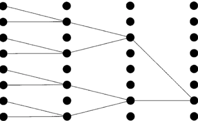
4. Digital Equivalents of Arbitrary Analog Systems Other elementary operations that are frequently used in analog Fourier optics are broadcast and integration. The equivalents of these operations can also be realized in log2N stages, as shown in
Figs. 3 and 4. Note that in realizing the equivalent of integration, addition is not performed by superpo-sition of light beams, but by the use of digital adders. Likewise, the equivalent of broadcast is realized in a tree manner for the sake of maintaining power levels. 1If sufficient power exists or if low signal-to-noise ratios can be tolerated, broadcast can actually be done in one stage by the optical replication of a single beam. Integration of moderate numbers of beams could also be done in one stage by the digital addition of the inputs from several optical detectors.2 These operations are useful, for instance, in realiz-ing matrix–vector product architectures.2
Now we show that the digital–optical equivalents of a general class of analog optical systems can be constructed. A rather general class of analog– optical systems is the class of so-called quadratic-phase systems.17,18 Optical systems involving an
arbitrary sequence of thin lenses and sections of free space belong to this class. They are characterized by the input–output relation 1for simplicity in one dimension2: fout1x2 5
e
2` ` C exp3ip1ax22 2bxx8 1 gx8224 f in1x82dx8, 112 where C is a complex constant, and a, b, and g arereal constants independent of x and x8. Imaging, Fourier transforming, free-space propagation, and passage through a lens are all special cases of the above. Now, it is known that1perhaps with appro-priate scaling of the transverse coordinates2 any such system can be decomposed in any of the following forms: qp1a, b, g2 5 lns1 f12 ft lns1 f22, 122 or qp1a, b, g2 5 lns1 f32 frft1a2 lns1 f42, 132 or qp1a, b, g2 5 lns1 f52 fs1d2 lns1 f62, 142
or still other forms.18–20 qp denotes a
quadratic-phase system, lns a lens, fs free-space propagation, ft a Fourier transform, and frft a fractional-order Fou-rier transform,18,21–25 with their parameters, focal
lengths 1 f 2, distance 1d2, order 1a2, etc., given in parentheses. Because we already have the equiva-lents of lenses and a Fourier transformer, Eq.122 will allow the realization of any quadratic-phase system 1including imaging systems, free-space propagation, etc.2.
Alternatively, instead of taking the Fourier trans-form as the basic building block, we can use free-space propagation or the fractional Fourier trans-form as the basic building block. Digital equivalents of free-space propagation and the fractional Fourier transform can both be realized by the use of ,log N-stage networks, which are not unlike that shown in Fig. 2. Then Eq.132 or Eq. 142 allows the realization of any quadratic-phase system. The es-sential point is that quadratic-phase systems can be decomposed into local operations that can be per-formed by the digital SLM’s and global operations that can be efficiently realized with free-space optics. 1The latter is possible because the connection pat-terns required for the global operations are suffi-ciently regular.3–52
Finally, we note that systems more general than quadratic-phase systems 3given by Eq. 1124 can be realized if any number of SLM’s 1programmable filters2 are sandwiched between any number of qua-dratic-phase systems. Because we know how to build digital equivalents of both the filters and the quadratic-phase systems, the equivalent of any ana-log Fourier optical system composed of lenses, filters, SLM’s, and sections of free space1including anamor-phic systems2 can be realized digitally. It is perhaps also worth noting that the ease with which complex spatial filtering is performed makes holography a redundant concept for digital systems. These digi-tal systems can perform any of the mathematical operations performed by real-time holograms in, for example, the Fourier plane. Complex numbers are equally well represented, stored, and operated on in the form of binary streams. 1However, this does not exclude the use of physical holographic elements in
Fig. 3. 1-D tree network for broadcast. The 2-D version is analogous.
Fig. 4. 1-D tree network for integration. The 2-D version is analogous.
realizing the physical optical connections of digital Fourier optics systems, such as the connections shown in Fig. 2.2
In some cases, it may be convenient to implement certain suboperations within a digital Fourier optics system by the use of true analog elements, instead of by replacing them also with their digital equivalents. For instance, it might be more simple to implement magnification by a simple optical imaging configura-tion. Because a one-to-one mapping is in question here, the digital nature of the signals are preserved, and the necessary dynamic range might be attained. 5. Discussion and Conclusion
The digital–optical systems being considered also have certain disadvantages with respect to their analog counterparts. Apart from the fact that the cost and the complexity of the optical system have greatly increased, we now have to wait at least of the order of log N times the intrinsic device delay Tdto perform a DFT, whereas in the analog case the delay was of the order of 1 3 Td. The bit rate of the signals passing through the systems is now limited by the speed of the optical devices, so that the system is no longer bandwidth transparent, but this is usually the case in conventional analog systems anyway, because of the input–output devices. 1An exception may be photonic-switching systems in which the input and the output are optical.2 Current technology suggests that these digital–optical sys-tems may be clocked at rates of 100 MHz or more. 1In fact, because the limitations associated with electronic input–output from the chip are elimi-nated, it may be well possible to run optically interconnected chips at clock rates higher than those of electrically interconnected chips. For example, Lentine et al.26 recently reported running 0.9-µm
silicon electronic circuits with optical input–output at 700 [email protected] Combined with unlimited accu-racy and cascadability and the ability to utilize substantial logical complexity in each optical pixel 1e.g., thousands of gates per pixel2, the loss of optical transparency is not considered a major disadvan-tage.
A more significant disadvantage is that the num-ber of pixels one can currently handle with digital systems is small compared with that of conventional analog systems. One reason for this is that yield considerations limit the size of the SEED arrays that can be built, a limitation that might be alleviated with improving technology. Based on previous expe-rience with SEED technology, it appears that thou-sands of optical pixels will be feasible, although this remains to be demonstrated. Another limitation is that greater tolerances must be satisfied by the optics that maps the spots of light from device plane to device plane, limiting attainable space–band-width products to values smaller than are common with analog systems. Multistage systems with thou-sands of beams per stage have, however, been demon-strated.8
For some applications, the smaller array of pixels that these systems can handle 1compared with ana-log systems2 may be sufficient. As one example, let us consider the highly successful image compression method known as transform-domain coding.12 In
this method the image is broken down into blocks 1subimages2, and each block is transformed indepen-dently. A typical size for these blocks is 8 3 8 pixels, amounting to 6425 4096 blocks for a 512 3 512 pixel
image. In general, choosing larger block sizes en-ables one to improve the amount of compression obtained. However, studies have shown that in-creasing the block size beyond 16 3 16 or 32 3 32 does not offer any further advantage.12 Thus the
optimal size of the blocks well matches the capabili-ties of the digital–optical systems discussed. Assum-ing 162 5 256 blocks of 32 3 32 pixels each, the
digital–optical system discussed above will require 256 3 160 ns 1 3.2 µs 5 44.2 µs to compute the transform of all blocks, whereas the electronic three DSP chip board will require 256 3 26 µs 5 6.7 ms.
For applications for which smaller arrays of pixels are not sufficient 1such as processing a 512 3 512 image as a whole2, one must explore means of overcoming this limitation. One approach is as follows. Because with developing submicrometer technology we can expect to have enough silicon circuitry to handle a far greater number of data pixels 1e.g., those of a sampled image2 than the available optical input–output pixels, we might con-sider the strategy of multiplexing the information belonging to several data pixels through a single optical connection. However, this will cause prob-lems if the information emanating from different data pixels wants to go to different places, an issue that must be explicitly considered. An alternative approach is to break the limit imposed by single arrays of SEED devices and single-lens imaging by the devising of ways of tiling these in the transverse dimension to realize effectively larger arrays 1as discussed in our numerical example above2.
In general, analog systems are useful in applica-tions that require the capacity to deal with a large number of pixels, but in which low-amplitude accu-racy and limited flexibility can be tolerated. Digital systems, on the other hand, can provide greater flexibility and amplitude accuracy, but can deal with a somewhat smaller number of pixels1although this may change if the above strategies are successful2. Digital systems also introduce a larger number of device delays compared with analog systems, but this issue should usually be secondary in deciding which approach to pursue for a given application. Throughput 1information processed per second2 is likely to be more important than latency1processing delay2 in many signal processing applications, as long as the delay is within reasonable bounds.
Another critical issue is the comparison of digital Fourier optical systems with fully electronic digital systems. Technologies for vertically integrating large numbers of silicon chips are now available.27
The density of vias in the vertical direction is much lower than the density of connections within the chip, but is comparable with the density of optical pinouts possible with the optoelectronic technology mentioned in this paper. Does this mean that one can always build the equivalent of a digital Fourier optical system by using such fully electronic vertical integration technologies? The answer is no. The vias in the mentioned electronic technologies provide direct connections only to the closest region of the next chip in the stack, whereas the optical system under consideration can provide global connections. The general principles of VLSI complexity theory and studies such as Refs. 15 and 16 clearly indicate that the ability to provide global connections will result in more efficient implementation of structures that require global information flow, such as the DFT, at least beyond a certain value of N. 1This does not exclude the use of vertical integration technologies to increase the amount of silicon avail-able per pixel, if needed, in digital Fourier optical systems.2 For a quantitative discussion and for consideration of applications that require intermedi-ate levels of globality, we refer the reader to the mentioned references.
Over the past 30 years, the elegance and the promise of analog Fourier optics have resulted in a large number of architectures and systems being proposed and studied.2 Some of these concentrated
on image processing1including pattern recognition2, some on algebraic processing1including matrix opera-tions2, and others on parallel processing 1including systolic and cellular systems2. Although some of the suggested systems became successful because the application was one whose requirements were well matched to the capabilities of an analog system, others failed because they required the accuracy or the flexibility of digital systems, which analog sys-tems could not provide. We believe that reconsidera-tion of digital Fourier optical versions of these systems and architectures will allow the potential of these concepts, architectures, and algorithms to be realized.
The primary research task in this area is the creation and the development of a flexible platform that allows the wide class of systems alluded to in this paper to be realized by the use of standard components and procedures.
We are pleased to acknowledge stimulating discus-sions with Joe Ford, Fouad Kiamilev, Ashok Krishnamoorthy, and Levent Onural.
References
1. J. W. Goodman, Introduction to Fourier Optics1McGraw-Hill, New York, 19682.
2. J. W. Goodman, ‘‘Four decades of optical information process-ing,’’ Opt. Photonics News 2122, 11–15 119912.
3. H. M. Ozaktas, Y. Amitai, and J. W. Goodman, ‘‘Comparison of system size for some optical interconnection architectures and the folded multi-facet architecture,’’ Opt. Commun. 82, 225–228119912.
4. H. M. Ozaktas and D. Mendlovic, ‘‘Multi-stage optical
intercon-nection architectures with least possible growth of system size,’’ Opt. Lett. 18, 296–298119932.
5. D. Mendlovic and H. M. Ozaktas, ‘‘Optical-coordinate transfor-mation methods and optical-interconnection architectures,’’ Appl. Opt. 32, 5119–5124119932.
6. See, for example, the special issue on smart pixels, S. R. Forrest and H. S. Hinton, eds., IEEE J. Quantum Electron.
29122, 119932.
7. See, for example, D. A. B. Miller, ‘‘Computing with light,’’ in 1995 Yearbook of Science and the Future1Encyclopedia Britan-nica, Chicago, 19942, pp. 134–147.
8. F. B. McCormick, T. J. Cloonan, A. L. Lentine, J. M. Sasian, R. L. Morrison, M. G. Beckman, S. L. Walker, M. J. Wojcik, S. J. Hinterlong, R. J. Crisci, R. A. Novotny, and H. S. Hinton, ‘‘Five-stage free-space optical switching network with field-effect transistor self-electro-optic-field-effect-device smart-pixel ar-rays,’’ Appl. Opt. 33, 1601–1618119942; H. S. Hinton, T. J. Cloonan, F. B. McCormick, A. L. Lentine, and F. A. P. Tooley, ‘‘Free-space digital optical systems,’’ Proc. IEEE 82, 1632– 1649119942.
9. K. S. Huang, C. B. Kuznia, B. K. Jenkins, and A. A. Sawchuk, ‘‘Parallel architectures for digital optical cellular image pro-cessing,’’ Proc. IEEE 82, 1711–1723119942.
10. K. W. Goossen, J. E. Cunningham, and W. Y. Jan, ‘‘GaAs 850 modulators solder-bonded to silicon,’’ IEEE Photonics Tech-nol. Lett. 5, 776–778119932; K. W. Goosen, J. A. Walker, L. A. D’Asaro, S. P. Hui, B. Tseng, R. Leibenguth, D. Kossives, D. D. Bacon, D. Dahringer, L. M. F. Chirovsky, A. L. Lentine, and D. A. B. Miller, ‘‘GaAs MQW modulators integrated with silicon CMOS,’’ IEEE Photonics Technol. Lett. 7, 360–362 119952.
11. F. Kiamilev and A. Krishnamoorthy, ‘‘Smart pixel designs for image processing,’’ in Photonics for Processors, Neural Net-works, and Memories II, J. L. Horner, B. Javidi, and S. T. Kowel, eds., Proc. Soc. Photo-Opt. Instrum. Eng. 2297, 37 119942.
12. A. K. Jain, Fundamentals of Digital Image Processing 1Pren-tice-Hall, Englewood Cliffs, N.J., 19892, p. 505.
13. S. G. Smith and P. B. Denyer, ‘‘Efficient bit-serial complex multiplication and sum-of-products computation using distrib-uted arithmetic,’’ in Proceedings of the International Confer-ence on Acoustics, Speech, and Signal Processing, 19861IEEE, New York, 19862, pp. 2203–2206.
14. R. F. Lyon, ‘‘Two’s complement pipeline multipliers,’’ IEEE Trans. Commun. 24, 418–425119762.
15. H. M. Ozaktas and J. W. Goodman, ‘‘Elements of a hybrid interconnection theory,’’ Appl. Opt. 33, 2968–2987119942. 16. A. V. Krishnamoorthy, P. J. Marchand, F. E. Kiamilev, and
S. C. Esener, ‘‘Grain-size considerations for optoelectronic multistage interconnection networks,’’ Appl. Opt. 31, 5480– 5507119922.
17. M. J. Bastiaans, ‘‘Wigner distribution function and its applica-tion to first-order optics,’’ J. Opt. Soc. Am. 69, 1710–1716119792. 18. H. M. Ozaktas and D. Mendlovic, ‘‘Fractional Fourier optics,’’
J. Opt. Soc. Am. A 12, 743–751119952.
19. A. Papoulis, Signal Analysis1McGraw-Hill, New York, 19772, p. 289.
20. M. Nazarathy and J. Shamir, ‘‘First-order optics—a canonical operator representation: lossless systems,’’ J. Opt. Soc. Am.
72, 356–364119822.
21. H. M. Ozaktas, B. Barshan, D. Mendlovic, and L. Onural, ‘‘Convolution, filtering, and multiplexing in fractional Fourier domains and their relation to chirp and wavelet transforms,’’ J. Opt. Soc. Am. A 11, 547–559119942.
22. A. W. Lohmann, ‘‘Image rotation, Wigner rotation, and the fractional Fourier transform,’’ J. Opt. Soc. Am. A 10, 2181– 2186119932.
Radon–Wigner and fractional Fourier transformations,’’ J. Opt. Soc. Am. A 11, 1798–1801119942.
24. L. B. Almeida, ‘‘The fractional Fourier transform and time-frequency representations,’’ IEEE Trans. Signal Process. 42, 3084–3091119942.
25. A. C. McBride and F. H. Kerr, ‘‘On Namias’s fractional Fourier transforms,’’ IMA J. Appl. Math. 39, 159–175119872.
26. A. L. Lentine, K. W. Goossen, J. F. Walker, L. M. F. Chirovsky, L. A. D’Asaro, B. Tseng, R. E. Leibenguth, D. Kossives, D.
Dahringer, D. D. Bacon, and T. K. Woodward, ‘‘700 Mb@s operation of optoelectronic switching nodes comprised of flip-chip-bonded GaAs@AlGaAs MQW modulators on silicon CMOS circuitry,’’ in Conference on Lasers and Electro-Optics, Vol. 15 of 1995 OSA Technical Digest Series1Optical Society of America, Washington, D.C., 19952, postdeadline paper CPD11. 27. M. J. Little and J. Grinberg, ‘‘The 3-D computer: an inte-grated stack of WSI wafers,’’ in Wafer-Scale Integration 1Kluwer, New York, 19882, Chap. 8.