COLLOIDAL HETEROSTRUCTURES OF
SEMICONDUCTOR QUANTUM WELLS:
SYNTHESIS, CHARACTERIZATION AND
APPLICATIONS
a dissertation submitted to
the graduate school of engineering and science
of bilkent university
in partial fulfillment of the requirements for
the degree of
doctor of philosophy
in
materials science and nanotechnology
By
Yusuf Kele¸stemur
June 2017
COLLOIDAL HETEROSTRUCTURES OF SEMICONDUCTOR QUANTUM WELLS: SYNTHESIS, CHARACTERIZATION AND APPLICATIONS
By Yusuf Kele¸stemur June 2017
We certify that we have read this dissertation and that in our opinion it is fully adequate, in scope and in quality, as a dissertation for the degree of Doctor of Philosophy.
Hilmi Volkan Demir (Advisor)
Evren Mutlug¨un
Emine Yegˆan Erdem
O˘guz G¨ulseren
Ahmet Macit ¨Ozenba¸s Approved for the Graduate School of Engineering and Science:
Ezhan Kara¸san
Director of the Graduate School iii
ABSTRACT
COLLOIDAL HETEROSTRUCTURES OF
SEMICONDUCTOR QUANTUM WELLS: SYNTHESIS,
CHARACTERIZATION AND APPLICATIONS
Yusuf Kele¸stemur
Ph.D. in Materials Science and Nanotechnology Advisor: Hilmi Volkan Demir
June 2017
Colloidal semiconductor quantum wells, also known as nanoplatelets (NPLs), have recently emerged as a new class of colloidal semiconductor nanocrystals enabling fascinating excitonic properties. With their quasi two-dimensional structure resembling epitaxially-grown quantum wells, these atomically-flat nanoplatelets exhibit narrow emission linewidths, giant linear and nonlinear ab-sorption cross-sections, and ultrafast fluorescence lifetimes when compared to other classes of semiconductor nanocrystals. These appealing features have led to achievement of low lasing thresholds and high color purity by using simple heterostructures of these NPLs. To further exploit the benefits of these solution-processed NPLs and develop next-generation colloidal optoelectronic devices, novel heterostructures of NPLs with superior excitonic properties are in high demand. In this thesis, to address these needs, we proposed and demonstrated novel heterostructured NPLs. This thesis includes the rational design and sys-tematic synthesis and characterization of these hetero-NPLs.
To overcome the lower photoluminescence quantum yield (PL-QY) and sta-bility issues of core/shell NPLs, we successfully synthesized CdSe/CdS/CdS core/crown/shell NPLs resembling platelet-in-a-box. With this advanced archi-tecture, we accomplished substantially enhanced PL-QY and absorption cross-section as well as stability, allowing for the achievement of low-threshold optical gain. However, due to the pure vertical confinement observed in these NPLs, these exciting excitonic features of NPLs suffered from the limited spectral tun-ability. By developing homogenously alloyed CdSexS1−x NPLs together with their
alloyed core/crown and alloyed core/shell heterostructures, we succeeded in ob-taining highly tunable excitonic features and further extending tunability of the optical gain from these NPLs. In addition to the NPLs having Type-I electronic structure, we demonstrated the highly uniform growth of CdSe/CdTe core/crown NPLs having Type-II electronic structure exhibiting unique excitonic properties.
v
Additionally, to realize the evolution of Type-II electronic structure, we synthe-sized CdSe/CdSe1−xTex core/crown NPLs by precisely tailoring the composition
of the crown region. Without changing their vertical thicknesses, we achieved again highly tunable excitonic features and near-unity PL-QY from these hetero-NPLs. Based on the proposed architectures of these heteronanoplatelets, we believe the findings of this thesis provide important guidelines and inspiration for the synthesis of highly efficient and stable heterostructured NPLs to construct high-performance colloidal optoelectronic devices, possibly challenging their con-ventional epitaxially-grown counterparts.
Keywords: Colloidal semiconductor nanocrystals, quantum wells, colloidal nanoplatelets, quantum dots, heterostructures.
¨
OZET
KOLO˙IDAL YARI˙ILETKEN KUANTUM
KUYULARININ HETEROYAPILARI:
SENTEZLENMES˙I, KARAKTER˙IZASYONU VE
UYGULAMALARI
Yusuf Kele¸stemur
Malzeme Bilimi ve Nanoteknoloji, Doktora Tez Danı¸smanı: Hilmi Volkan Demir
Haziran 2017
Son zamanlarda nanolevhalar olarak da bilinen koloidal yarıiletken kuantum kuyuları, b¨uy¨uleyici eksitonik ¨ozellikleri ile kolloidal yarıiletken nanokristallerin yeni bir sınıfı olarak ortaya ¸cıkmı¸stır. Epitaksiyal olarak b¨uy¨ut¨ulm¨u¸s kuan-tum kuyularına benzeyen iki boyutlu yapısıyla, atomik d¨uzeyde yassı olan bu nanolevhalar di˘ger kolloidal yarıiletken nanokristallerle kar¸sıla¸stırıldıklarında dar ı¸sıma aralıklarına, ¸cok y¨uksek do˘grusal ve do˘grusal olmayan so˘gurma kesit-lerine ve olduk¸ca hızlı ı¸sıma ya¸sam s¨urelerine sahiptirler. Bu dikkat ¸cekici ¨
ozellikler, bu nanolevhaların basit yapıları kullanılarak d¨u¸s¨uk e¸sik de˘gerine sahip optik kazan¸c ve y¨uksek renk saflı˘gı elde edilmesini sa˘glamı¸stır. Bu kolloidal nanolevhaların faydalarından daha fazla yararlanmak ve yeni nesil optoelektronik aygıtları geli¸stirmek i¸cin, ¨ust¨un eksitonik ¨ozellik g¨osteren yenilik¸ci mimarilere sahip nanolevhalar b¨uy¨uk ra˘gbet g¨ormektedir. Bu tezde, bu ihtiya¸cları kar¸sılamak i¸cin, yenilik¸ci mimari yapılara sahip nanolevhaları ¨onerdik ve g¨osterdik. Bu tez, bu heteroyapıların rasyonel tasarımı, sistematik sentezi ve karakterizasyonunu i¸cermektedir.
C¸ ekirdek/kabuk mimarisine sahip nanolevhaların d¨u¸s¨uk ı¸sıma verimlili˘gi ve dayanıklılık sorunlarını gidermek i¸cin, kutu i¸cinde kuantum levha mi-marisini andıran CdSe/CdS/CdS ¸cekirdek/ta¸c/kabuk nanolevhalarını ba¸sarıyla sentezledik. Bu geli¸smi¸s yapıya sahip nanolevhaların, ı¸sıma verimliliklerini, so˘gurma kesitlerini ve dayanıklılıklarını ¨onemli ¨ol¸c¨ude geli¸stirerek, d¨u¸s¨uk e¸sik de˘gerine sahip optik kazan¸c elde edilmesini sa˘gladık. Ancak, bu nanolevhalarda sadece dikey boyutta g¨ozlemlenen kuantum sınırlamasından dolayı, koloidal nanolevhaların bu heyecan verici eksitonik ¨ozellikleri sınırlı bir spektral aralıkta elde edilebilmi¸stir. Tezde, ala¸sımlı ¸cekirdek/ta¸c ve ala¸sımlı ¸cekirdek/kabuk yapıları ile birlikte homojen olarak ala¸sımlanmı¸s CdSexS1−x nanolevhalarını
vii
geli¸stirerek, ¸cok geni¸s bir spektral aralıkta ayarlanabilir eksitonik ¨ozellikler elde etmeyi ve bu nanolevhalardan elde edilen optik kazancın spektral aralı˘gını geni¸sletmeyi ba¸sardık. Tip-I elektronik yapıya sahip nanolevhalara ek olarak, e¸ssiz eksitonik ¨ozellikler sergileyen Type-II elektronik yapıya sahip olan CdSe/CdTe ¸cekirdek/ta¸c nanolevhalarını ¸cok d¨uzg¨un bir ¸sekilde sentezlenmesini de g¨osterdik. Ayrıca, Type-II elektronik yapısının olu¸sumunu detaylı bir ¸sekilde incelemek i¸cin, ta¸c b¨olgesinin kompozisyonunu kontrollu bir ¸sekilde ayarlayarak, CdSe/CdSe1−xTex ¸cekirdek/ta¸c nanolevhalarını sentezledik. Nanolevhaların
dikey kalınlıklarını de˘gi¸stirmeden, geni¸s bir spektral aralıkta ayarlanabilen ek-sitonik ¨ozellikler elde ettik ve bu yapıya sahip nanolevhalarla y¨uzde y¨uze yakın ı¸sıma verimlili˘gine ula¸stık. ¨Onerilen farklı mimarilere sahip nanolevhalar ile bir-likte bu tezin bulgularının, y¨uksek performans g¨osterebilen kolloidal optoelek-tronik cihazlar in¸sa etmekte kullanılacak y¨uksek verimlili˘ge ve dayanıklılı˘ga sahip nanolevhaların sentezi i¸cin ¨onemli bir kılavuz ve ilham kayna˘gı olaca˘gına inanıyoruz. Bu geli¸smi¸s yapıya sahip olan koloidal nanolevhalar muhtemelen epi-taksiyal olarak b¨uy¨ut¨ulen ve yaygın bir ¸sekilde kullanılan kuantum kuyularına kar¸sı ileride ¸cok g¨u¸cl¨u bir rakip olacaktır.
Anahtar s¨ozc¨ukler : Koloidal yarıiletken nanokristaller, kuantum kuyuları, koloidal nanolevhalar, kuantum noktacıkları, heteroyapılar.
Acknowledgement
First, I would like to thank my supervisor Prof. Hilmi Volkan Demir. With his kind, positive, friendly, and warm personality and his invaluable guidance, motivation, immense knowledge and endless support, he has been more than a supervisor for me. During my graduate study, I learned a lot from him about both academic and social life, which was invaluable for me.
I would like to thank my thesis monitoring committee members Assoc. Prof. Evren Mutlugun and Asst. Prof. Emine Yegan Erdem for their valuable com-ments and discussion. I would like to sincerely thank my jury members Prof. Oguz Gulseren and Prof. Ahmet Macit Ozenbas for being on my PhD jury and for their remarks and suggestions.
This thesis would not be possible without the support and contribution from my close friends and colleagues. I am thankful to the past and present members of Demir Research Group. Especially, I would like to thank Dr. Evren Mutlugun, who always shares his knowledge and experience with me both research and life. I would also like to thank Ozgun Akyuz, Emre Unal, Dr. Burak Guzelturk, Dr. Talha Erdem, Kivanc Gungor, Dr. Sedat Nizamoglu, Dr. Emre Sari, Dr. Rohat Melik, Dr. Can Uran, Dr. Zeliha Soran Erdem, Dr. Aydan Yeltik, Ahmet Fatih Cihan, Shahab Akhavan, Onur Erdem, Didem Dede, Nima Taghipour, Dr. Urartu Ozgur Safak Seker, Dr. Nihan Kosku Perkgoz, Dr. Pedro Ludwig Hernandez-Martinez, Dr. Vijay Kumar Sharma, Dr. Manoj Sharma, Ashma Sharma, Dr. Murat Olutas, Dr. Savas Delikanli, Dr. Akbar Alipour, Mehmet Zafer Akgul, Berkay Bozok, Halil Akcali, Ibrahim Akcali, Cuneyt Eroglu, Onur Akin, Dr. Mustafa Akin Sefunc, Yasemin Coskun, Sayim Gokyar, Dr. Veli Tayfun Kilic, Refik Sina Toru, Hatice Ertugrul, Dr. Durmus Ugur Karatay, Ozan Yerli, Togay Amirahmadov, Birsen Bilgili, and Can Firat Usanmaz. I will never forget their friendship and great times that we had in our highly close-packed office. Also, I would like to thank all the professors, graduate students, technical and administrative staff at UNAM. I would like to also thank Mustafa Guler for his support and help in TEM imaging.
I must express my very profound gratitude to my dear-wife and love Emel. She has always made my life colorful. I would like to thank her for providing
ix
me with unfailing support and continuous encouragement throughout my years of graduate study. I would like to thank my lovely family: my father Bedrettin, my mother Fatma, my elder sister Unzile, and my brother Mirac for their love, endless support and encouragement. They have been always with me whenever I need them.
Finally, I would like to thank TUBITAK BIDEB and SPIE for the financial support.
x
Contents
Chapter 1 ... 1
Introduction ... 1
1.1 Organization of the Thesis ... 4
Chapter 2 ... 6
Colloidal Semiconductor Nanocrystals ... 6
2.1 Basic Concepts of Semiconductor Nanocrystals ... 7
2.2 Colloidal Synthesis of Semiconductor Nanocrystals ... 10
2.3. Different Heterostructures of Semiconductor Nanocrystals ... 14
2.3.1 Nanocrystals with Type-I Heterostructures ... 16
2.3.2 Nanocrystals with Type-II Heterostructures ... 20
2.3.3 Nanocrystals with Quasi Type-II Heterostructures ... 21
2.4. Colloidal Quantum Wells ... 23
Chapter 3 ... 32
Characterization of Colloidal Quantum Wells ... 32
3.1 Optical Characterization Techniques... 32
3.1.1 Steady-State Absorption Spectroscopy ... 33
3.1.2 Steady-State Photoluminescence Spectroscopy ... 35
3.1.3 Photoluminescence Excitation Spectroscopy ... 36
3.1.4 Photoluminescence Quantum Yield Measurements ... 39
3.1.5 Time-Resolved Fluorescence Spectroscopy ... 43
3.2 Structural Characterization Techniques ... 45
3.2.1 Transmission Electron Microscopy ... 45
3.2.2 X-Ray Photoelectron Spectroscopy ... 49
3.2.3 X-Ray Diffraction ... 51
Chapter 4 ... 54
xi
4.1 Motivation ... 54
4.2 Colloidal Synthesis and Experiments ... 58
4.3 Results and Discussion ... 61
4.4 Summary ... 83
Chapter 5 ... 85
CdSexS1-x Alloyed Heteronanoplatelets ... 85
5.1 Motivation ... 85
5.2 Colloidal Synthesis and Experiments ... 88
5.3 Results and Discussion ... 92
5.4 Summary ... 109
Chapter 6 ... 111
CdSe/CdTe Core/Crown Heteronanoplatelets ... 111
6.1 Motivation ... 111
6.2 Colloidal Synthesis and Experiments ... 114
6.3 Results and Discussion ... 118
6.4 Summary ... 136
Chapter 7 ... 137
CdSe/CdSe1-xTex Core/Crown Heteronanoplatelets ... 137
7.1 Motivation ... 137
7.2 Colloidal Synthesis and Experiments ... 140
7.3 Results and Discussion ... 143
7.4 Summary ... 164
Chapter 8 ... 165
Conclusion ... 165
8.1 Concluding Remarks ... 165
8.2 Future Outlook ... 168
8.3 Contributions to the Literature ... 169
xii
List of Figures
Figure 2.1. Schematic illustration of band diagrams in bulk semiconductors and colloidal semiconductor NCs. While continuous band diagrams are observed in the bulk semiconductors, colloidal semiconductor NCs exhibit quantized energy levels in their band structure. Also, with decreasing the size of the colloidal semiconductor NCs, their effective band gap energy is increased. ... 8 Figure 2.2. (a) Schematic drawing of a colloidal semiconductor NC composed of inorganic core and organic ligands together with (b) a representative high-resolution transmission electron microscopy image of a single colloidal semiconductor NC, synthesized at our laboratories. (c) Normalized absorption and photoluminescence spectra of colloidal CdSe NCs having different diameters showing their strongly tunable excitonic properties, synthesized at our laboratories. ... 9 Figure 2.3. The nucleation and growth model describing colloidal synthesis of highly monodisperse NCs proposed by La Mer together with schematic drawing of a typical colloidal synthesis setup. Reprinted with permission from [27]. ... 13 Figure 2.4. Core/shell heterostructures of colloidal semiconductor NCs having different band alignment (Type-I, quasi Type-II and Type-II) along with the localization of electron and hole wavefunctions in these architectures. ... 16 Figure 2.5. (a) Schematic drawing of the core/shell NC having chemical composition gradient structure together with their band alignment. (b) Normalized photoluminescence spectra of blue-, green- and red-emitting colloidal NCs with the chemical composition gradient structure, synthesized at our laboratories. ... 19 Figure 2.6. (a) High-resolution transmission electron microscopy (TEM) image of our CdSe/CdS core/shell NCs showing highly monodisperse size distribution. (b) Normalized absorption and photoluminescence spectra of our CdSe/CdS core/shell NCs with narrow emission linewidths (~28 nm). ... 23 Figure 2.7. High-angle annular dark-field scanning transmission electron microscopy (HAADF-STEM) image of our colloidal NPLs with the inset showing the schematic drawing of atomically-flat colloidal NPLs. ... 24 Figure 2.8. Normalized (a) absorption and (b) photoluminescence spectra of our 4 ML thick CdSe core NPLs. HAADF-STEM images of our 4 ML thick CdSe core NPLs with varying lateral dimensions from (c) rectangular-shaped to (d) almost square-shaped. . 27 Figure 2.9. Normalized absorption and photoluminescence spectra of our CdSe colloidal NPLs having different vertical thicknesses, synthesized at our laboratories. ... 28
xiii
Figure 2.10. (a) Schematic drawings of core-only colloidal NPLs together with their core/crown (laterally grown shell) and core/shell (vertically grown shell) heterostructures. Normalized absorption and photoluminescence spectra of (b) our CdSe/CdS core/crown and (c) core/shell NPLs, all of which are synthesized at our laboratories. ... 29 Figure 3.1. Normalized absorption spectra of our CdSe core-only NPLs having different vertical thicknesses, synthesized at our laboratories. ... 34 Figure 3.2. Normalized absorption spectra of (a) CdSe/CdS core/crown NPLs and (b) CdSe/CdS core/shell NPLs with different vertical thicknesses synthesized at our laboratories. ... 35 Figure 3.3. Normalized photoluminescence spectra of CdSe core-only NPLs with varying vertical thicknesses synthesized at our laboratories. ... 36 Figure 3.4. (a) Normalized photoluminescence and photoluminescence excitation spectra of our 4 ML thick CdSe core NPLs together with their absorption spectra. (b) The photoluminescence excitation spectra of our 4 ML thick CdSe core NPLs taken at different emission wavelengths. ... 37 Figure 3.5. Photoluminescence excitation spectra of (a) CdSe/CdS core/shell and (b) CdSe/CdTe core/crown NPLs taken at different emission wavelengths synthesized at our laboratories. ... 39 Figure 3.6. (a) Schematic demonstration of different measurement configurations used in the absolute PL-QY measurement method. Reproduced with permission from [92]. Copyright Royal Society of Chemistry 2015. (b) PL-QY measurements of CdSe/CdSe1-xTe1-x core/crown NPLs (x = 0.10) performed by following the absolute
PL-QY measurements method at our laboratories. While the higher energy sides of the emission spectra show the excitation spectra obtained in different measurement configurations, the lower energy sides of the spectra belong to the emission spectra of the sample obtained in different measurement configurations. ... 42 Figure 3.7. Time-resolved fluorescence decays curves of (a) CdSe core and CdSe/CdS core/crown NPLs having Type-I electronic structure and (b) CdSe core and CdSe/CdTe core/crown NPLs having Type-II electronic structure. These core and core/crown heterostructured NPLs were synthesized at our laboratories. ... 44 Figure 3.8. HAADF-STEM images of 4 ML thick CdSe core NPLs having (a) rectangular shape and (b) square shape, which were synthesized at our laboratories. .. 47 Figure 3.9. HAADF-STEM images of (a) 4 ML thick CdSe core-only NPLs and (b) 4 ML thick CdSe/CdTe core/crown NPLs. (c) HAADF-STEM image of a single CdSe/CdTe core/crown NPL together with with blue (Y−Yl) and green lines (X−Xl)
showing the EDX probe position. The line EDX analysis reporting the compositions of selenium and tellurium in the core/crown NPLs within (e) blue (Y−Yl) and (f) green lines
(X−Xl). All of these NPLs presented here were synthesized at our laboratories. Reprinted
xiv
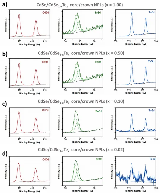
Figure 3.10. The acquired high-resolution XPS spectra of the CdSe/CdSe1-xTex
core/crown NPLs with varying crown compositions; (a) x = 1.00, (b) x = 0.50, (c) x = 0.10 and (d) x = 0.02, synthesized at our laboratories. Reprinted with permission from [93]. Copyright 2017 American Chemical Society. ... 50 Figure 3.11. Powder XRD patterns of 4 ML thick CdSe core NPLs and CdSe/CdSe1-xTex
core/crown NPLs having different crown compositions synthesized at our laboratories. Reprinted with permission from [93]. Copyright 2017 American Chemical Society. .. 52 Figure 4.1. (a) Normalized absorption and photoluminescence spectra of CdSe core-only NPLs and (b) HAADF-STEM image of CdSe core-only NPLs. Reprinted with permission from [94]. Copyright 2016 WILEY-VCH Verlag GmbH & Co. KGaA, Weinheim. ... 62 Figure 4.2. (a) Normalized absorption and photoluminescence spectra of CdSe core and
CdSe/CdS core/crown NPLs having different crown sizes. Normalized
photoluminescence excitation spectra of (b), (c) and (d) CdSe/CdS core/crown NPLs having different crown sizes taken at different emission wavelengths. Reprinted with permission from [94]. Copyright 2016 WILEY-VCH Verlag GmbH & Co. KGaA, Weinheim. ... 64 Figure 4.3. HAADF-STEM images of (a) CdSe core-only and CdSe/CdS core/crown NPLs with (b) small, (c) medium, and (d) large CdS crown size. Reprinted with permission from [94]. Copyright 2016 WILEY-VCH Verlag GmbH & Co. KGaA, Weinheim. ... 65 Figure 4.4. Normalized absorption and photoluminescence spectra of (a) CdSe@CdS core@shell, and (b) CdSe/CdS@CdS core/crown@shell NPLs with varying CdS shell thicknesses. Reprinted with permission from [94]. Copyright 2016 WILEY-VCH Verlag GmbH & Co. KGaA, Weinheim. ... 66 Figure 4.5. HAADF-STEM images of (a), (b) and (c) the CdSe/l_CdS@CdS core/crown@shell NPLs having 2 ML CdS shell thickness at different magnifications. High-resolution TEM image of the CdSe/l_CdS@CdS core/crown@shell NPLs having 2 ML CdS shell is given in the inset. Reprinted with permission from [94]. Copyright 2016 WILEY-VCH Verlag GmbH & Co. KGaA, Weinheim. ... 68 Figure 4.6. Photoluminescence excitation spectra of (a) CdSe/CdS core/crown NPLs having medium crown size and CdSe/CdS@CdS core/crown@shell NPLs having (b) 1 ML CdS shell, (c) 2 ML CdS shell and (d) 3 ML CdS shell taken at different emission wavelengths. Reprinted with permission from [94]. Copyright 2016 WILEY-VCH Verlag GmbH & Co. KGaA, Weinheim. ... 70 Figure 4.7. Time-resolved fluorescence spectroscopy measurements of (a) CdSe core-only NPLs and CdSe/CdS core/crown NPLs with varying CdS crown size, (b) CdSe@CdS core@shell NPLs, and (c) CdSe/CdS@CdS core/crown@shell NPLs with different CdS shell thicknesses. (d) Amplitude-averaged fluorescence lifetime of the core, core/crown, core@shell, and core/crown@shell NPLs having different CdS crown
xv
sizes as a function of the shell thickness. Reprinted with permission from [94]. Copyright 2016 WILEY-VCH Verlag GmbH & Co. KGaA, Weinheim. ... 73 Figure 4.8. Temperature dependent PL spectra of (a) CdSe@CdS core@shell NPLs and (b) CdSe/CdS@CdS core/crown@shell NPLs having 2 ML CdS shell thicknesses. Amplitude-averaged fluorescence lifetimes (τav) of these (c) core@shell and (d)
core/crown@shell NPLs at the lower energy side, at the higher energy side and at the maximum of emission. Reprinted with permission from [94]. Copyright 2016 WILEY-VCH Verlag GmbH & Co. KGaA, Weinheim. ... 77 Figure 4.9. Optical gain performances of CdSe-based NPLs having different architectures. Amplified spontaneous emission spectra of (a) CdSe core-only NPLs, (b) CdSe@CdS core@shell NPLs having 2 ML CdS shell thickness, (c) CdSe/CdS core/crown NPLs, and (d) CdSe/CdS@CdS core/crown@shell NPLs having 2 ML CdS shell thickness. The insets show the integrated PL intensity as a function of the excitation intensity. Reprinted with permission from [94]. Copyright 2016 WILEY-VCH Verlag GmbH & Co. KGaA, Weinheim. ... 81 Figure 4.10. Intensity of the amplified spontaneous emission in the core/crown@shell NPLs as a function of pump laser shots (per pulse energy density of 35 µJ/cm2). The
optical gain in the core/crown@shell NPLs is highly stable even for 6 h of continuous excitation. Reprinted with permission from [94]. Copyright 2016 WILEY-VCH Verlag GmbH & Co. KGaA, Weinheim. ... 83 Figure 5.1. (a) HAADF-STEM images of CdSexS1-x alloyed core NPLs having different
sulfur compositions, (b) high-resolution X-ray photoelectron spectra of spin-coated thin films of CdSexS1-x alloyed core NPLs, (c) normalized absorbance and
photoluminescence (PL) spectra of CdSexS1-x alloyed core NPLs, showing continuous
blue-shifted excitonic features, (d) photoluminescence excitation spectra of CdSexS1-x
alloyed core NPLs. Reprinted with permission from [112]. Copyright 2017 American Chemical Society. ... 93 Figure 5.2. Normalized photoluminescence excitation spectra of CdSexS1-x NPLs taken
at different emission wavelengths with various sulfur compositions (a) x = 0.0, (b) x = 0.85, (c) x = 0.75, and (d) x = 0.70. Reprinted with permission from [112]. Copyright 2017 American Chemical Society. ... 95 Figure 5.3. (a) HAADF-STEM images of CdSexS1-x/CdS alloyed core/crown NPLs
having different sulfur compositions, (b) normalized absorbance and photoluminescence spectra of CdSexS1-x/CdS core/crown NPLs and (c) time-resolved fluorescence decay
curves of CdSexS1-x alloyed core and CdSexS1-x/CdS core/crown NPLs for the case of
x = 0.75. Reprinted with permission from [112]. Copyright 2017 American Chemical Society. ... 97 Figure 5.4. Time-resolved fluorescence decay curves of CdSexS1-x/CdS core/crown
NPLs together with their core for the case of (a) x = 1.00, (b) x = 0.85, (c) x = 0.75 and (d) x = 0.70. Reprinted with permission from [112]. Copyright 2017 American Chemical Society. ... 99
xvi
Figure 5.5. (a) HAADF-STEM images of CdSexS1-x/CdS core/shell NPLs having 3 ML
CdS shell thicknesses, (b) normalized absorbance spectra of CdSexS1-x/CdS core/shell
NPLs with different sulfur composition and CdS shell thicknesses, (c) PL spectra of CdSexS1-x/CdS core/shell NPLs with varying sulfur composition and CdS shell
thicknesses, and (d) time-resolved fluorescence decay curves of CdSexS1-x alloyed core
and CdSexS1-x/CdS core/shell NPLs having 3 ML CdS shell for the case of x = 0.75 (d).
Reprinted with permission from [112]. Copyright 2017 American Chemical Society. ... 101 Figure 5.6. Time-resolved fluorescence decay curves of CdSexS1-x/CdS core/shell NPLs
having 3 ML CdS shell together with their core for the case of (a) x = 1.00, (b) x = 0.85, (c) x = 0.75, and (d) x = 0.70. Reprinted with permission from [112]. Copyright 2017 American Chemical Society. ... 104 Figure 5.7. Optical gain performances of CdSexS1-x/CdS core/crown and core/shell NPLs
having different sulfur compositions. As an exemplary case for x = 0.75 amplified spontaneous emission spectra of (a) CdSexS1-x core-only NPLs, (b) CdSexS1-x/CdS
core/crown NPLs, (c) CdSexS1-x/CdS core/shell NPLs having 2 ML CdS shell at different
excitation fluence. In the insets, the integrated PL intensity are given as a function of the pump fluence. (d) Normalized ASE spectra of CdSexS1-x/CdS heterostructures showing
highly tunable gain performance varying with the incorporated sulfur amount. Reprinted with permission from [112]. Copyright 2017 American Chemical Society. ... 107 Figure 6.1. (a) Normalized absorption and photoluminescence spectra of 4 ML thick CdSe NPLs dissolved in hexane. (b) HAADF-STEM images of the 4 ML thick CdSe NPLs with a scale bar of 50 nm. Reprinted with permission from [95]. Copyright 2015 American Chemical Society. ... 119 Figure 6.2. Optical characterization of 4 ML thick CdSe/CdTe core/crown NPLs having a higher PL-QY. (a) Schematic representation of carrier photogeneration in both CdSe core and the CdTe crown regions, transfer to core/crown interface, and subsequent radiative recombination resulting in Type-II emission. (b) Normalized absorption, (c) normalized photoluminescence, and (d) normalized photoluminescence excitation spectra of the CdSe/CdTe core/crown NPLs dissolved in hexane with varied crown size. Reprinted with permission from [95]. Copyright 2015 American Chemical Society. 121 Figure 6.3. Structural characterization of 4 ML thick CdSe/CdTe core/crown NPLs having a higher PL-QY. HAADF-STEM images of CdSe/CdTe core/crown NPLs with a scale bar of (a) 100 and (b) 50 nm. (c) HAADF-STEM image of a single CdSe/CdTe core/crown NPL, with blue (Y−YI) and green lines (X−XI) showing the EDX probe position on CdSe/CdTe core/crown NPL and (d, e) the line EDX analysis reporting the compositions of selenium and tellurium in the CdSe/CdTe core/crown NPL, normalized to the total anionic composition. Reprinted with permission from [95]. Copyright 2015 American Chemical Society. ... 124
xvii
Figure 6.4. X-ray diffraction pattern of 4 ML thick CdSe core NPLs and 4 ML thick CdSe/CdTe core/crown NPLs. Reprinted with permission from [95]. Copyright 2015 American Chemical Society. ... 125 Figure 6.5. Time-resolved fluorescence decay curves of the CdSe/CdTe core/crown NPLs having (a) a higher PL-QY and (b) lower PL-QY with varied crown size. The amplitude-averaged fluorescence lifetimes of CdSe/CdTe core/crown NPLs having (c) a higher PL-QY and (d) lower PL-QY. Reprinted with permission from [95]. Copyright 2015 American Chemical Society. ... 127 Figure 6.6. (a) Temperature-dependent time-resolved fluorescence decay curves of the CdSe/CdTe core/crown NPLs having a higher PL-QY and (b) their amplitude-averaged fluorescence lifetime. Reprinted with permission from [95]. Copyright 2015 American Chemical Society. ... 132 Figure 6.7. Normalized absorption spectra of (a) 4 ML thick CdSe core NPLs and (b) 4 ML thick CdSe/CdTe core/crown NPLs before and after the ligand exchange. Reprinted with permission from [95]. Copyright 2015 American Chemical Society. ... 135 Figure 7.1. (a) Absorption (solid line) and photoluminescence (dotted−dashed line) spectra and (b) HAADF-STEM images of the 4 ML thick CdSe core-only NPLs dissolved in hexane at room temperature, having a lateral size of 16.4 ± 1.7 nm by 12.6 ± 1.5 nm. Reprinted with permission from [93]. Copyright 2017 American Chemical Society. ... 144 Figure 7.2. (a) Normalized absorption, (b) photoluminescence and (c) photoluminescence excitation spectra of CdSe/CdTe core/crown NPLs having different CdTe crown size. Reprinted with permission from [93]. Copyright 2017 American Chemical Society. ... 146 Figure 7.3. HAADF-STEM images of the CdSe/CdSe1−xTex core/crown NPLs for
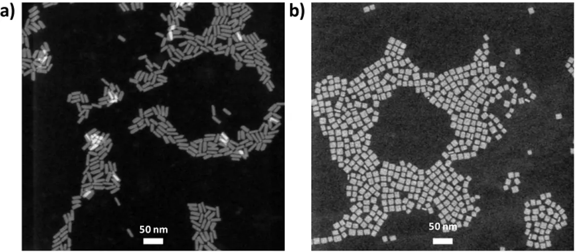
different Te compositions (a) x = 1.00, (b) x = 0.75, (c) x = 0.50, and (d) x = 0.25 in the crown region. Reprinted with permission from [93]. Copyright 2017 American Chemical Society. ... 148 Figure 7.4. HAADF-STEM images of the CdSe/CdSe1−xTex core/crown NPLs for
different Te compositions (a) x = 0.10, (b) x = 0.05, and (c) x = 0.02 in the crown region. Reprinted with permission from [93]. Copyright 2017 American Chemical Society. 149 Figure 7.5. HAADF-STEM image of a single CdSe/CdSe1-xTex core/crown NPL with
blue (Y−Yl) and green lines (X−Xl) showing the EDX probe position on core/crown NPL together with their line EDX analysis reporting the compositions of selenium and tellurium in the CdSe/CdSe1-xTex core/crown NPL, having different crown compositions
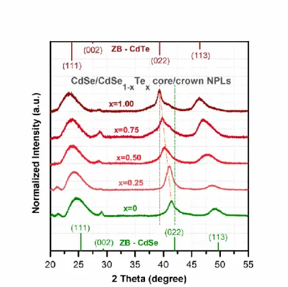
(a) x = 1.00, (b) x = 0.50, and (c) x= 0.25. Reprinted with permission from [93]. Copyright 2017 American Chemical Society. ... 151 Figure 7.6. X-ray diffraction patterns of the 4 ML thick CdSe core-only NPLs and the CdSe/CdSe1−xTex core/crown NPLs having different crown compositions. The green (on
xviii
and bulk CdTe having zinc blende (ZB) structure, respectively. Reprinted with permission from [93]. Copyright 2017 American Chemical Society. ... 154 Figure 7.7. (a) Evolution of the absorption and photoluminescence spectra along with PL-QY as a function of the CdSe1−xTex crown region composition. (b) The real color
images of CdSe/CdSe1−xTex core/crown NPLs having different crown compositions
dissolved in hexane under UV light (top) and ambient light (bottom). (c) Photoluminescence excitation spectra of the CdSe/CdSe1−xTex core/crown NPLs
together with their photoluminescence and (d) extracted band gap energy of the crown region as a function of the composition of the Te in the crown. Reprinted with permission from [93]. Copyright 2017 American Chemical Society. ... 156 Figure 7.8. Photoluminescence excitation spectra of CdSe/CdSe1-xTex core/crown NPLs
having different crown composition taken at different emission wavelength. Reprinted with permission from [93]. Copyright 2017 American Chemical Society. ... 158 Figure 7.9. Schematic demonstration of band diagrams of the CdSe/CdSe1−xTex
core/crown NPLs (a) for x ≥ 0.25, and (b) for x ≤ 0.10. (c) Time-resolved fluorescence decay curves of the CdSe core and CdSe/CdSe1−xTex core/crown NPLs for different
crown region compositions (e.g., x = 1.00, 0.50, and 0.10). The solid lines on the decay curves represent the four-exponential fitting curves. (d) Amplitude-averaged fluorescence lifetimes of the CdSe/CdSe1−xTex core/crown NPLs with tuned crown
compositions. Reprinted with permission from [93]. Copyright 2017 American Chemical Society. ... 162 Figure 7.10. Emission spectra of the NPL-integrated LED at varying currents along with luminous efficiency (LE) (inset, right) and CIE 1931 color coordinates (inset, left). Reprinted with permission from [93]. Copyright 2017 American Chemical Society. 163
xix
List of Tables
Table 5.1. Analysis of time-resolved fluorescence decay curves of CdSexS1-x alloyed
core NPLs with different sulfur composition. Reprinted with permission from [112]. Copyright 2017 American Chemical Society. ... 100 Table 5.2. Analysis of time-resolved fluorescence decay curves of CdSexS1-x/CdS
core/crown NPLs with different sulfur composition. Reprinted with permission from [112]. Copyright 2017 American Chemical Society... 100 Table 5.3. Analysis of time-resolved fluorescence decay curves of CdSexS1-x core NPLs
used for the CdS shell coating. Reprinted with permission from [112]. Copyright 2017 American Chemical Society. ... 105 Table 5.4. Analysis of time-resolved fluorescence decay curves of CdSexS1-x/CdS
core/shell NPLs having 3 ML CdS shell. Reprinted with permission from [112]. Copyright 2017 American Chemical Society. ... 105 Table 6.1. Numerical analysis of time-resolved fluorescence from CdSe/CdTe core/crown NPLs having a lower PL-QY with different CdTe crown widths. Reprinted with permission from [95]. Copyright 2015 American Chemical Society. ... 128 Table 6.2. Numerical analysis of time-resolved fluorescence from CdSe/CdTe core/crown NPLs having a higher PL-QY with different CdTe crown widths. Reprinted with permission from [95]. Copyright 2015 American Chemical Society. ... 129 Table 6.3. Numerical analysis of temperature-dependent time-resolved fluorescence from CdSe/CdTe core/crown NPLs having a higher PL-QY. Reprinted with permission from [95]. Copyright 2015 American Chemical Society. ... 133 Table 7.1. Lateral dimensions of CdSe/CdSe1-xTex core/crown NPLs having different
crown compositions obtained from the HAADF-STEM images. Reprinted with permission from [93]. Copyright 2017 American Chemical Society. ... 150 Table 7.2. Chemical composition of CdSe/CdSe1-xTex core/crown NPLs having different
crown compositions obtained from the XPS. Reprinted with permission from [93]. Copyright 2017 American Chemical Society. ... 153 Table 7.3. Chemical composition of CdSe1-xTex crown region obtained from the XPS.
Reprinted with permission from [93]. Copyright 2017 American Chemical Society. 153 Table 7.4. Chemical composition of CdSe1-xTex crown region obtained from the XRD.
1
Chapter 1
Introduction
One of the characteristic features of semiconductor materials is their energy gap between the fully-occupied valence band and unoccupied conduction band. With their relatively lower energy gap (< 2-3 eV) enabling the harnessing of light, semiconductors have become indispensable for the field of optoelectronics. The strong interaction of semiconductors with light including its generation, detection and management has paved the way to utilize novel light-emitting and -harvesting optoelectronic devices for a broad range of applications spanning from the information technologies and life sciences to the lighting and displays technologies. For further exploiting the benefits of optoelectronics, a new class of materials have been strongly desired offering highly tunable excitonic properties together with the ability of fabricating low-cost, large-area and ultra-flexible devices. While the current semiconductor technology has shown great success in the fabrication of small-area and/or chip-scale devices under the ultra-high vacuum conditions, the fabrication of large-area and ultra-flexible devices would not be achievable in a cost-effective way by using the current technology. Also, the commonly used semiconductors have suffered from the limited tunability of their excitonic features.
At this point, colloidal semiconductor nanocrystals (NCs) stand out as a promising class of materials with their fascinating excitonic properties [1]–[3]. With the quantum
2
confinement effect observed in these tiny nanocrystals, they exhibit highly tunable optical properties and electronic structures, which can be controlled simply by tailoring their size, shape and compositions [4]. Also, the synthesis of free-standing semiconductor NCs using a relatively simple and robust colloidal approach has enabled the engineering of different heterostructures of NCs with desired excitonic properties for the development of the solution-processed optoelectronic devices [5]–[7]. With the considerable progress in the understanding of the physical chemistry of semiconductor NCs together with their excitonic properties, the first products of these tiny nanocrystals have been recently announced with the introduction of semiconductor NCs based displays offering dramatically improved color quality and efficiency [8], [9]. These pioneering products have proved the significant potential of colloidal semiconductor NCs to revolutionize optoelectronic technology and trigger the development of various colloidal NCs based light-emitting and light-harvesting optoelectronic devices including light-emitting diodes (LEDs) [10], lasers [11], photovoltaic cells [12], detectors [13] and luminescent solar concentrators (LSCs) [14]. Thus, to utilize the benefits of these optoelectronic devices, great efforts have been devoted to the development of colloidal semiconductor NCs with superior excitonic properties.
Recently, colloidal semiconductor quantum wells, also known as colloidal nanoplatelets (NPLs), have arisen as a novel class of colloidal semiconductor NCs and attracted a lot of attention with their remarkable excitonic properties [15], [16]. With their two-dimensional (2D) structure [17], resembling the epitaxially-grown quantum wells, these solution-processed NPLs exhibit the narrowest emission linewidths (< 35-40 meV), giant oscillator strength, ultrafast radiative lifetime and extremely large absorption cross-section. Also, with the colloidal synthesis of core/crown [18] and
3
core/shell [19] NPLs, their excitonic properties have been further improved to achieve enhanced device performances. To date, record low lasing thresholds [20] and LEDs with high color quality [21] have been demonstrated by using these heterostructures of atomically-flat NPLs, surpassing the performance of other classes of colloidal semiconductor nanocrystals. These great successes achieved by using these primitive heterostructures of colloidal quantum wells has shown their great potential for the achievement of solution-processed optoelectronic devices and emphasized the necessity of the novel heterostructured NPLs.
To address these needs, in our thesis, we have focused on the design, synthesis and characterization of novel heterostructured colloidal NPLs to obtain superior excitonic properties, enabling the development of high-performance optoelectronic devices. We have proposed and synthesized solution-processed colloidal NPLs with novel heterostructures such as core/crown/shell NPLs by precisely controlling their size, shape and composition. We have verified the growth of highly uniform and crystalline NPLs with well-defined shape and compositions by using structural characterization tools employing transmission electron microscopy, Ray photoelectron spectroscopy and X-Ray diffraction. Their resulting excitonic properties have been also investigated with
optical spectroscopy techniques including steady-state absorption and
photoluminescence spectroscopy, photoluminescence excitation spectroscopy, and time-resolved fluorescence spectroscopy. Our findings have shown that that carefully heterostructured NPLs will play a critical role in the development of future high-performance colloidal optoelectronic devices, which may even possibly challenge their traditional epitaxially grown thin-film based counterparts.
4
1.1 Organization of the Thesis
In Chapter 2, we present the basic concepts about colloidal semiconductor nanocrystals including their size-dependent optical properties and electronic structures, their synthesis and different heterostructures. We also introduce the colloidal quantum wells, emerging as a new class of colloidal semiconductor nanocrystals.
In Chapter 3, we present the characterization techniques used for the detailed investigation of the structural and optical properties of the synthesized NPLs with unique heterostructures.
In Chapter 4, we report the synthesis of CdSe/CdS/CdS core/crown/shell NPLs having a novel three-dimensional heterostructure resembling platelet-in-box structure together with their optical and structural characterization. We also present their highly stable and low-threshold optical gain performance.
In Chapter 5, we describe the synthesis of alloyed CdSexS1-x core NPLs with their
core/crown and core/shell heterostructures. These alloyed heterostructured NPLs exhibit highly tunable excitonic properties, enabling the achievement of amplified spontaneous emission at varied wavelengths.
In Chapter 6, we introduce the synthesis and characterization CdSe/CdTe core/crown heterostructured NPLs having Type-II electronic structure. Here, we present their unique excitonic properties significantly different than NPLs having Type-I electronic structures.
5
In Chapter 7, we present the synthesis and characterization of CdSe/CdSexTe1-x
core/crown NPLs with precisely controlled crown composition. We report the highly tunable excitonic properties achieved in these heterostructured NPLs without changing their thicknesses.
6
Chapter 2
Colloidal Semiconductor Nanocrystals
This thesis work involves the synthesis, characterization and applications of novel heterostructures of colloidal nanoplatelets, emerging as a new class of colloidal semiconductor nanocrystals. In this chapter, before presenting our findings and related discussion, we would like to provide background information about colloidal semiconductor nanocrystals for the ease of understanding subsequent chapters. We start with the basics concepts about the colloidal NCs including their size-dependent electronic structures and optical properties. Subsequently, we continue with the colloidal synthesis of these tiny crystalline semiconductors and their different heterostructures. Finally, we conclude this chapter with the colloidal nanoplatelets, showing exciting excitonic properties when compared to the other classes of semiconductor nanocrystals.
7
2.1 Basic Concepts of Semiconductor
Nanocrystals
Colloidal semiconductor nanocrystals can be defined as tiny crystalline semiconductors consisting of hundreds to thousands of atoms with a typical diameter ranging from 2 to 20 nm [2], [3]. With the quantum confinement effects observed at this length scale, these tiny crystals exhibit unique size-dependent electronic structure and optical properties significantly different from their bulk counterparts [4], [22]. In the bulk semiconductors, a large density of covalently and/or ionically bonded atoms give rise the formation of continuous energy levels in the conduction and valence bands, which are separated with a fixed band gap energy depending on the composition and crystal structure of the semiconductor material (Figure 2.1) [1]. On the other hand, semiconductor NCs composed of finite number of atoms possess atomic-like discretized energy levels with a tunable effective band gap energy, which can be controlled by simply changing their size and shape [1]. The effective band gap energy of semiconductor nanocrystals can be increased by decreasing their size, enabling a wide coverage range of electromagnetic spectrum by using a single material system having the same chemical compositions.
8
Figure 2.1. Schematic illustration of band diagrams in bulk semiconductors and colloidal semiconductor NCs. While continuous band diagrams are observed in the bulk semiconductors, colloidal semiconductor NCs exhibit quantized energy levels in their band structure. Also, with decreasing the size of the colloidal semiconductor NCs, their effective band gap energy is increased.
Upon the excitation of semiconductors with photons having higher energies than their band gap, electron and hole pairs are formed, which are known as excitons. However, owing to higher dielectric constant of the bulk semiconductors, generated electron and hole pairs feature small Columbic binding energy and they generally act as free carriers [6]. On the other hand, in the semiconductor NCs having a comparable and/or smaller size than the exciton Bohr radius, the quantum and dielectric confinement effects give rise to increased exciton binding energy and strongly modify their excitonic properties [3], [6]. With the increased exciton binding energy, semiconductor NCs exhibit strongly
BULK SEMICONDUCTORS COLLOIDAL SEMICONDUCTOR NANOCRYSTALS
Conduction Band (CB)
Valence Band (VB) Energy Band Gap
(EBG) EBG EBG EBG CB CB CB VB VB VB CB VB
9
enhanced excitonic absorption features with broad absorption spectrum (Figure 2.2). Thanks to their discrete energy levels, these NCs feature narrow emission linewidth with wide spectral tunability. Also, they possess improved photoluminescence quantum yield (PL-QY) together with faster fluorescence lifetime. Moreover, these tiny crystalline semiconductors composed of inorganic cores and organic ligands have excellent photostability and chemical stability when compared to their organic counterparts [23].
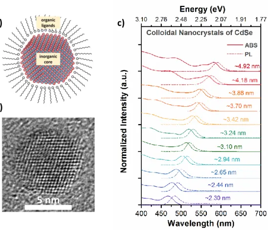
Figure 2.2. (a) Schematic drawing of a colloidal semiconductor NC composed of inorganic core and organic ligands together with (b) a representative high-resolution transmission electron microscopy image of a single colloidal semiconductor NC, synthesized at our laboratories. (c) Normalized absorption and photoluminescence
5 nm
a)
b)
10
spectra of colloidal CdSe NCs having different diameters showing their strongly tunable excitonic properties, synthesized at our laboratories.
In addition to the these exciting excitonic properties of colloidal semiconductor NCs, their solution process-ability make them highly appealing for the development of the next-generation light-emitting and light-harvesting optoelectronic device applications. The colloidal dispersion of semiconductor NCs enables the development of low-cost, large-scale, ultra-flexible and functional optoelectronic devices with the solution-processed fabrication techniques [7], [24]. However, to utilize the great potential for the achievement of superior device performance, the synthesis of high-quality semiconductor NCs is the key.
2.2 Colloidal Synthesis of Semiconductor
Nanocrystals
With the realization of quantum confinement effect in semiconductors enabling the size and shape tuning of the optical properties and electronic structures, synthesis of semiconductor NCs has attracted increasingly great attention and become one of the most promising research problems in the colloidal community within the last three decades. The first observation of quantum confinement effect in semiconductor crystals was reported by Ekimov [25]. This early work demonstrated that nano-sized semiconductor crystals grown in the glass medium exhibit size-dependent excitonic absorption behaviors. Also, with the synthesis of different sized nano-colloids, size-dependent electronic structures and optical properties were shown by Brus [26]. Although these pioneering studies successfully demonstrated the quantum confinement
11
effect in semiconductor crystals, a major challenge was to obtain highly crystalline, monodisperse and isolated semiconductor NCs for a full understanding of their unique excitonic properties and exploiting their potential in novel device architectures.
This goal was eventually achieved with the colloidal synthesis of highly monodisperse, uniform and crystalline CdSe, CdS and CdTe semiconductor NCs by the group of Bawendi [4]. With the co-injection of organometallic precursors into a hot coordinating solvent, sudden nucleation of semiconductor crystallites was achieved from its supersaturated solution. Subsequently, it was followed with the separate growth stage, leading to formation of highly monodisperse and uniform shaped colloidal semiconductor NCs in the presence of organic ligands in the reaction solution. This relatively simple and novel approach for the synthesis of semiconductor NCs has made a major breakthrough in the field of colloidal chemistry and inspired the community for the synthesis of different kinds of nanomaterials.
A typical colloidal synthesis of semiconductor NCs is composed of three basic components: molecular precursors, ligands and solvents [27]–[29]. Molecular precursors are decomposed into monomers at higher reaction temperatures and supply the required materials for the nucleation and growth of nanocrystals. Their reactivity can be also tuned by changing molecular side groups [30]. Another important component of the colloidal synthesis is the ligands, which are organic molecules commonly used to achieve uniformity and monodispersity [31]. They are dynamically attached to the surface of the nanocrystals and play a critical role for the determination of their final size and shape [32], [33]. Also, these organic molecules are responsible for the colloidal stability of nanoparticles to form a stable dispersion. Finally, solvents used in the
12
colloidal synthesis enable the complete dissolution of molecular precursors to form a homogenous reaction mixture. In addition, together with ligands, they are accounted for the colloidal stability of nanocrystals in the reaction mixture. With the appropriate selection of molecular precursors, ligands and solvents, highly crystalline semiconductor NCs can be synthesized by using colloidal approaches [28], [34].
In addition to the appropriate selection of chemicals, the understanding of the nucleation and growth kinetics in colloidal synthesis is highly crucial for the achievement of highly monodisperse and uniform semiconductor NCs. With the proposed nucleation and growth model by La Mer [35], it was shown that separation of nucleation and growth stages is highly required to achieve monodispersity in the colloidal synthesis (Figure 2.3). To obtain discrete nucleation and growth stages, supersaturated solution is formed with the fast injection of molecular precursor into the hot reaction solution. With the decomposition of the molecular precursors in the reaction solutions, the monomer concentrations exceed the critical limit for the homogenous nucleation and small size crystallites are nucleated rapidly. During the fast nucleation step, the monomer concentrations are consumed significantly and decreased below the critical limit for the homogenous nucleation, eliminating the formation probability of new nuclei. Then, it is followed by a separate growth stage of almost identical size seed nanocrystals, allowing the formation of uniform colloidal nanocrystals with a highly monodisperse size distribution.
13
Figure 2.3. The nucleation and growth model describing colloidal synthesis of highly monodisperse NCs proposed by La Mer together with schematic drawing of a typical colloidal synthesis setup. Reprinted with permission from [27].
The growth stage in the colloidal synthesis can be also analyzed in two separate steps [36]. In the early stage of the growth, in the case of relatively higher monomer concentration in the reaction solution, smaller size nanocrystals grow at a faster rate with respect to the larger ones, leading to the decreased size distribution. On the other hand, with the depletion of monomer concentration in the final stage of the growth, smaller size nanocrystals start to dissolve due to their higher surface energy, while bigger size nanocrystals start to grow, resulting in the increased size distribution. This process is
14
called as Ostwald ripening and controlling the Ostwald ripening during the colloidal synthesis is highly critical to achieve highly monodisperse colloidal semiconductor NCs.
A better understanding of reaction kinetics together with the expanded chemical library by developing less toxic and highly stable molecular precursors have enabled colloidal synthesis to become highly robust, allowing for a simple approach for the synthesis of different kinds of semiconductor NCs. Starting with the successful synthesis of II–VI group compounds including CdSe, CdS and CdTe [37] nanocrystals, colloidal approach is further extended to the synthesis of III–V group compounds such as InP [38], [39] and InAs [39] nanocrystals and IV–VI group compounds including PbS [40], PbSe [41], and PbTe [42] nanocrystals. In addition to the core-only semiconductor nanocrystal having spherical shape, different kinds of semiconductor nanocrystals with mixed dimensionalities and various heterostructures have been also synthesized using colloidal approach for further engineering their excitonic properties [43]–[47].
2.3. Different Heterostructures of Semiconductor
Nanocrystals
With decreasing the size of nanocrystals, the ratio of the surface-to-volume atoms reaches significantly higher levels and this dramatically affects the resulting optical properties of colloidal semiconductor NCs [2]. While the atoms residing inside the nanocrystals have complete numbers of bonding with surrounding atoms, the surface atoms seriously suffer from the incomplete numbers of bonding and/or dangling bonds, diminishing their performance. Although the surface of colloidal NCs is covered with the organic ligands for the passivation of dangling bonds, these organic molecules may
15
not be able to supply complete chemical and electronic passivation for the semiconductor NCs. For example, core-only semiconductor nanocrystals are quickly deteriorated when exposed to the atmospheric conditions due to the oxidation. Also, generated electron and hole pairs in core-only nanocrystals can be trapped by the surface atoms, resulting in the decreased PL-QY.
For the achievement of proper chemical and electronic stabilization of colloidal semiconductor NCs, heterostructured nanostructures composed of inorganic core and epitaxially grown inorganic shell have been designed and studied [48]. In addition to the effective passivation of surface atoms with the formation epitaxially grown shell, heterostructured semiconductor NCs offer great opportunities for further engineering the excitonic properties of nanocrystals by controlling the band alignment between the core and shell (Figure 2.4) [49].
For the core/shell heterostructures having Type-I like band alignment, electron and hole wavefunctions are confined in the same region of the structures, resulting in the increased wavefunction overlap and enhanced radiative recombination probability [50]. These enhanced radiative recombination rates observed in NCs with Type-I electronic structure make them highly appealing for light-emitting optoelectronic device applications. On the other hand, for the core/shell heterostructures having Type-II like band alignment, electron and hole wavefunctions are localized in the separate regions of the NCs, leading to decreased wavefunction overlap and reducing the radiative recombination probability [51]. These heterostructures are quite interesting for the light-harvesting optoelectronic applications including solar cells and photodetectors.
16
Figure 2.4. Core/shell heterostructures of colloidal semiconductor NCs having different band alignment (Type-I, quasi Type-II and Type-II) along with the localization of electron and hole wavefunctions in these architectures.
2.3.1 Nanocrystals with Type-I Heterostructures
The first successful demonstrations of core/shell heterostructured NCs having Type-I electronic structure were reported by growing CdS and/or ZnS shell layers on top of the CdSe cores [50], [52], [53]. With the formation of larger band gap CdS and ZnS shell layers around CdSe core, electron and hole wavefunctions were confined mostly to the core region. In addition, enhanced surface passivation of CdSe cores with the shell coating improved PL-QY (up to 40-50%) and enhanced stability in these heterostructured NCs. Also, these core/shell NCs exhibit continuously red-shifting
-+ -+ -+ +
Core/Shell Heterostructures of Colloidal Semiconductor Nanocrystals
Type-I Band Alignment Quasi Type-II Band Alignment Type-II Band Alignment
17
emission with increasing the thickness of shell layer, which is explained with the relaxation of the quantum confinement.
The colloidal synthesis of these core/shell heterostructured NCs was performed in two separate steps. In the first step, high-quality CdSe core NCs were synthesized and used as a seed for the subsequent shell overcoating after purification. In the second step, with the slow addition of shell precursors into the reaction mixture, the CdS and/or ZnS shell layers were epitaxially grown on CdSe core NCs. Here, the concentration of shell precursors, the injection rate of shell precursors and the shell growth temperature are highly important parameters to be optimized, avoiding the homogenous nucleation of shell precursors.
For further eliminating the risk of homogenous nucleation during the shell growth, successive ion layer adsorption and reaction (SILAR) technique was developed by the group of Peng [54]. By using this approach, they demonstrated the synthesis of large-scale and highly monodisperse CdSe/CdS core/shell colloidal NCs. With the alternating injection of certain amount of shell precursors into the reaction mixture, SILAR technique reduces the probability of homogenous nucleation of shell materials and offer highly precise shell thickness control. Therefore, with precisely adjusting the CdS shell thickness, they showed successfully tunable emission behavior from CdSe/CdS core/shell NCs. Moreover, thanks to the versatility of SILAR technique, it was further extended to the synthesis of multishell heterostructures, which is strongly required to achieve ideal semiconductor NC having highly crystalline structure and well-passivated electronic structure suppressing the tunneling of electrons and holes from core region to surface trap sites.
18
While CdSe/CdS core/shell material system features lower lattice mismatch enabling the formation of highly crystalline nanocrystals, they suffer from the incomplete electronic passivation owing to the lower energy barrier for the electrons [55]. On the other hand, CdSe/ZnS system exhibits improved electronic passivation with respect to CdSe/CdS core/shell NCs owing to the higher band gap of ZnS [55]. However, higher lattice mismatch observed in this material system leads to increased strain formation, creating trap sites. Therefore, carefully designed heterostructured nanocrystals are strongly required to achieve superior properties by combining the advantages of different materials.
The first demonstrations of multishell heterostructures were demonstrated with the synthesis of CdSe/CdS/ZnS core/multishell NCs [55], [56]. By growing a thin layer of CdS shell between the CdSe core and ZnS shell, formation of highly crystalline NCs was obtained with these multishell heterostructures, reducing strain formation. In addition to that, the proper electronic passivation by using both CdS and ZnS shell layers enabled the achievement of improved PL-QY (up to 70-85%) with enhanced photostability. This initial study has shown the critical importance of the multishell heterostructures and inspired the community for further investigation of various multishell architectures using simple and low-cost colloidal synthesis techniques.
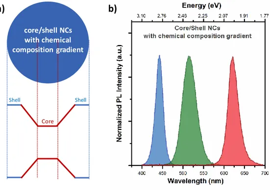
To address these needs, one-pot synthesis of highly crystalline and efficient core/shell NCs was developed [57]. By using the reactivity difference between the precursors, the formation of both core and shell was achieved in a single-step synthesis. The resulting core/shell semiconductor NCs had a chemical structure with composition gradient, strongly improving their crystal quality and reducing strain formation (Figure 2.5a).
19
Also, the chemical composition gradient strongly modified their electronic structures, enabling the funneling of excitons into the core region and increasing the radiative recombination rates. With their promising chemical and electronic structures, these NCs possessed higher photoluminescence quantum yield (up to 85-95%) and excellent photostability. In addition, by simply adjusting the amount of the initial precursors, highly efficient blue-, green- and red-emitting semiconductor NCs can be obtained using this one-pot synthesis approach (Figure 2.5b) [58], [59].
Figure 2.5. (a) Schematic drawing of the core/shell NC having chemical composition gradient structure together with their band alignment. (b) Normalized photoluminescence spectra of blue-, green- and red-emitting colloidal NCs with the chemical composition gradient structure, synthesized at our laboratories.
Shell Shell Core core/shell NCs with chemical composition gradient
a)
b)
20
The strategies developed for the achievement of highly crystalline and efficient core/shell heterostructures having Type-I electronic structure was successfully extended to the colloidal synthesis of Cd- and/or heavy metal free NCs. It was shown that InP/ZnS [60], [61] and CuInS2/ZnS [62], [63] core/shell NCs with higher photoluminescence
quantum yield (reaching ~80%) can be also synthesized by using colloidal routes. With the higher PL-QY and enhanced photostability, core/shell heterostructures of Type-I nanocrystals have been widely used for the development of novel light-emitting optoelectronic device applications including LEDs and lasers.
2.3.2 Nanocrystals with Type-II Heterostructures
In addition to the colloidal nanocrystals having Type-I electronic structure, semiconductor NCs with Type-II electronic structure have offered unique and exciting excitonic properties [64]. With the localization of electron and hole wavefunctions in the separate regions of NCs, spatially indirect excitons are formed at the core/shell interface. With the radiative recombination of these spatially indirect excitons, they exhibit strongly red-shifted emission, which would not be accessible from a single core and/or shell material. Also, owing to the reduced overlap of the electron and hole wavefunctions in these heterostructures, they feature decreased PL-QY with elongated radiative lifetime. In addition, the reduced electron and hole wavefunction overlap enables the suppression of nonradiative Auger recombination. These appealing properties of core/shell heterostructures having Type-II band alignment make them highly promising for the light-harvesting optoelectronic applications, including solar cells and photodetectors.
21
The first demonstrations of colloidal NCs having Type-II electronic structure was shown with the synthesis of CdTe/CdSe and CdSe/ZnTe core/shell heterostructures by the group of Bawendi [51]. For both samples, strongly red-shifted emissions were observed with elongated radiative lifetimes, suggesting the formation of Type-II electronic structures. Additionally, the order of core and shell materials strongly affect excitonic properties of the resulting core/shell nanocrystal having Type-II electronic structures. For example, although both CdSe/CdTe and CdTe/CdSe core/shell heterostructures exhibit Type-II like band alignment, their emission and absorption behaviors were rather different, showing the importance of the starting core material. Furthermore, different kinds of semiconductor NCs with Type-II electronic structures including CdS/ZnSe [65] and ZnSe/ZnTe [66] were synthesized to further tune their absorption and emission behaviors.
2.3.3 Nanocrystals with Quasi Type-II Heterostructures
Colloidal semiconductor NCs with quasi Type-II electronic structure lying within the Type-I and Type-II heterostructures have also shown interesting optical properties. Owing to the similar energy levels observed in the conduction and/or valence bands between the core and shell materials, the partial separation of electron and hole pairs are obtained in these heterostructures. Among the limited numbers of material pairs having quasi Type-II band alignment, CdSe/CdS core/shell heterostructures have been the most widely studied material system [67]. With the lower energy barrier for electrons in this material system, electrons are localized through the whole structure (both the core and shell regions), while holes are confined to the CdSe core. Therefore, with the partial separation of electron and hole wavefunctions, suppression of nonradiative Auger
22
recombination was observed in these heterostructures. Also, the lower lattice mismatch between the CdSe and CdS materials enables the uniform growth of thick CdS shell with a reduced number of defect sites, boosting their photostability. Furthermore, the relatively lower band of CdS with respect to ZnS make a great contribution to the enhancement of the absorption cross-section in these NCs. With these appealing features, CdSe/CdS core/shell heterostructures have been investigated extensively for the development of highly stable nanocrystal LEDs and low-threshold lasers.
The initial studies on the synthesis of CdSe/CdS core/shell heterostructures with thick CdS shell (up to 20 monolayers of shell) were performed by using SILAR technique offering highly precise shell thickness control [67], [68]. Owing to the formation of thick CdS shell, these heterostructures are also known as “giant” nanocrystals. With the formation of CdS shell, these giant nanocrystals exhibit improved absorption cross-section and strongly red-shifted emission with suppressed blinking behavior [69]. Also, thanks to the reduced rate of Auger recombination in these giant core/shell nanocrystals, high-performance LEDs [70] and low-threshold gain [71] were achieved. However, the formation of thick CdS shell over a long time period and the abrupt interface at the core/shell boundary have hampered the achievement of superior performance with these heterostructures.
To further push their performance and improve the PL-QY, the synthesis of CdSe/CdS core/shell NCs having alloyed and/or gradient shell structures has been targeted. Recently, colloidal synthesis of high-quality CdSe/CdS core/shell NCs has been demonstrated with narrow emission linewidth and suppressed blinking [72]. With the slow growth rate of CdS shell at higher temperature, highly uniform and crystalline
23
core/shell NCs were achieved resulting in the near-unity PL-QY (Figure 2.6). Also, the higher shell growth temperature led to the formation of smooth CdSexS1-x interface
owing to the enhanced interdiffusion between the core and shell regions, reducing Auger recombination rates. These CdSe/CdS core/shell heterostructures with relatively thin CdS shell (6-7 monolayers) and smooth interface had superior excitonic properties when compared to colloidal nanocrystals having similar size and enabled the achievement of low-threshold gain and lasing under two-photon optical pumping [73].
Figure 2.6. (a) High-resolution transmission electron microscopy (TEM) image of our CdSe/CdS core/shell NCs showing highly monodisperse size distribution. (b) Normalized absorption and photoluminescence spectra of our CdSe/CdS core/shell NCs with narrow emission linewidths (~28 nm).
2.4. Colloidal Quantum Wells
Thanks to the advancements in the field of the colloidal chemistry, the synthesis of semiconductor nanocrystals starting with the spherical shaped nanocrystals has been
50 nm
24
extended to the more anisotropic and complex structures including nanorods and tetrapods [45]–[47]. Recently, synthesis of atomically-flat colloidal nanoplatelets NPLs have been also demonstrated by using colloidal approaches [15]. These colloidal NPLs feature lateral dimensions on the order of tens of nanometers with the atomic-scale vertical thickness, which can be controlled precisely with the synthesis (Figure 2.7). Also, owing to their similarity with the epitaxially grown quantum wells, these colloidal NPLs are called as colloidal quantum wells.
Figure 2.7. High-angle annular dark-field scanning transmission electron microscopy (HAADF-STEM) image of our colloidal NPLs with the inset showing the schematic drawing of atomically-flat colloidal NPLs.
The first synthesis of these atomically-flat NPLs were demonstrated by the group of Dubertret [15]. These colloidal CdSe NPLs having zinc blende crystal structure were synthesized with precisely controlled vertical thicknesses by slightly changing the recipe
20 nm