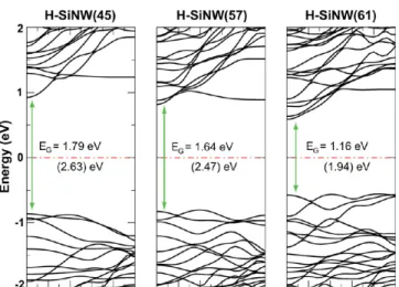
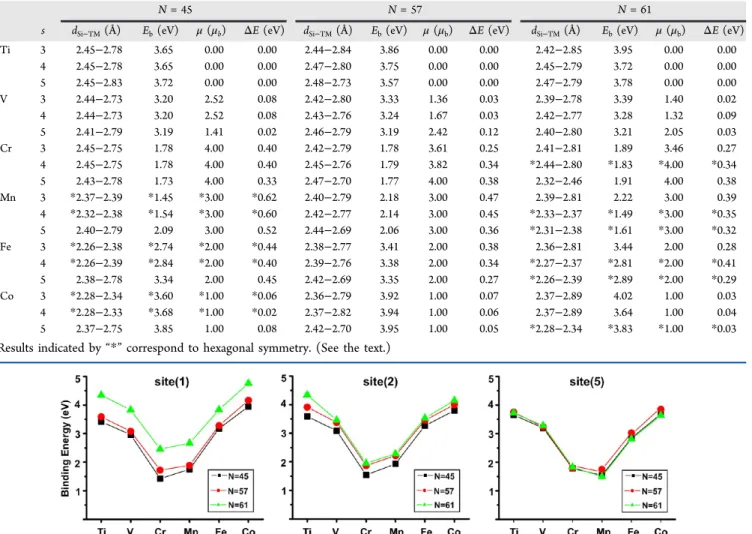
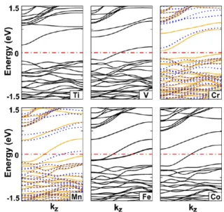
Hydrogen-saturated silicon nanowires heavily doped with interstitals and substitutional transition metals
Tam metin
Şekil


Benzer Belgeler
Experiments that compared the slide-level predictions of the classifiers with the reference data showed average precision values up to 62% when the training and validation data
In the special case when the demands for products are statistically independent, the first-order optimality condition for a product will depend on only the demand and cost parameters
Electronic properties of the superlattice such as HH–LH splitting energies was investigated using first principles calculations taking into account InSb and AlAs as possible
In this paper, we investigated the distributional impact of the post-1970 accumulation patterns and technological change in the Turkish manufacturing industries. Our
This analysis of pronominal referencing of Turkish L2 academic writing may serve as baseline study against which repeat studies among speakers of other languages, especially
Şekil 4 incelendiğinde, araştırma kapsamına alınan doktora tezlerinin %63.1’i erken okuryazarlık becerilerinin ev ortamında desteklenmesinde ebeveynlerin aktif
For this purpose, we first employ a term-based approach and formulate the chat mining problem as an automated text classification problem, in which the words occurring in chat
Abstract – We study theoretically the electronic transport in parallel few-level quantum dots in the presence of both intradot and interdot long-range Coulomb interaction.. Each dot
