Pinhole-Free PbS Thin Film Production Using a Low-Temperature
Chemical Bath Deposition Method
Metehan Önal
1,a, Barış Altıokka
1,b1Bilecik Şeyh Edebali University, Bilecik 11210 Turkey a[email protected], b[email protected] 1Tel: +90 228 214 1596–1596 Fax: +90 228 214 1332 2Tel: +90 228 214 1607–1607 Fax: +90 228 214 1332
Keywords: chemical bath deposition; PbS; thin films; interval time
Abstract. In this study, PbS thin films were produced at a low temperature such as 15Cᵒ using the chemical bath deposition (CBD) method.0.0085 M Pb (NO3)2 and 0.1460 M NaOH were dissolved in 100ml deionized water. 0.510 M thiourea which would be added to the solution was divided into 10 portions and added at zero, two, four, six and eight-minute intervals. Structural analysis of the obtained samples was carried out from XRD patterns which showed a significant increase in the peak intensity of the films obtained by adding thiourea at intervals of four and six minutes. The surface morphologies of the films were analyzed using a scanning electron microscope. According to the SEM images, when thiourea was added to the solution at intervals of four minutes, no cracks and holes were formed on the surfaces of the films obtained.
Introduction
Metal sulfide-based binary thin-film semiconductors have been attracting considerable interest as an efficient material for solar energy conversion owing to their versatile optical and electrical properties [1]. Lead sulfide (PbS) is an important binary IV-VI semiconductor material
[2]. It is a direct narrow-gap semiconductor material, and it has an energy band range of about 0.4 eV at 300K [3]. It forms in a galena structure which is a lead sulfide mineral with a chemical
composition of PbS[4].
Lead sulfide is in the center of attention due to its enormous applications in the field of optoelectronic such as solar cell, infrared (IR) detection, quantum dot sapplications, and selective coating for photo thermal conversion [5].
For synthesizing PbS, there are various methods including spray pyrolysis, pulsed laser deposition, vacuum evaporation, chemical vapor deposition (CVD), chemical bath deposition (CBD), ultrasound deposition, and electrodeposition [6]. Of these methods, CBD is based on successive adsorption and reaction of species on the substrate surface from aqueous solutions. It does not need complex or expensive instruments [7].In the CBD, the action process for forming lead sulfide films is considered as follows [8];
Pb (NO3)2+ 2NaO →Pb (OH)2+ 2NaNO3 (1)
Pb (OH)2+ 4NaOH → Na4Pb (OH)6 (2)
Na4Pb (OH)6→ 4Na+ + HPbO-2+ 3OH + H2O (3)
SC (NH2)2+ OH- → CH2N2+ H2O + SH- (4)
HPbO-2+ SH-→ PbS + 2OH- (5)
In the literature, PbS thin films were produced at several temperatures such as 25ᵒC [5,9,10], 40ᵒC [6],and 60-90ᵒC [11]. In addition, there weren’t any studies that utilized a bath temperature below 25ᵒC.
All rights reserved. No part of contents of this paper may be reproduced or transmitted in any form or by any means without the written permission of Trans Tech Publications Ltd, www.scientific.net. (#540996552, University of Wollongong, Wollongong, Australia-18/07/20,15:45:36)
In our study, the temperature of the deionized water was measured as 15ᵒC under laboratory conditions. It was also seen in the literature that the studies were conducted at temperatures of 25ᵒC and above; so obviously water had to be heated to reach these temperatures which caused energy loss. However, it was found that the film surface produced at the low temperature of 15ᵒC was covered with cracks and pinholes. Within our study, we managed to solve this problem by adding thiourea at different time intervals.
1. Experimental Details
To produce PbS thin films by the chemical bath deposition method, 0.0085 M Pb (NO3)2 and
0.1460 M NaOH were dissolved in 100 ml deionized water. After that, 0.510 M thiourea was divided into 10 equal portions and added to the solution at intervals of zero, two, four, six, and eight minutes. Before starting the deposition process, the bath container and glass substrate were washed with acetone and W/W 5% hydrochloric acid. After the washing, the glass substrate and bath container were rinsed with deionized water. After all chemicals were added to the bath container, each experiment was completed in 45 minutes. The temperature of the solution was measured as 15ᵒC during the depositions.
The samples were labeled as DT0, DT2, DT4, DT6 and DT9 according to the delay time of adding thiourea at zero, two, four, six, and eight minutes, respectively. While the first sample (DT0) was produced, 0.510M thiourea was added directly to the final solution and stirred with a magnetic stirrer at 600 rpm for 45 minutes. While DT2, DT4, DT6 and DT8 were produced, the thiourea was divided into 10 equal portions and added to the final solution at intervals of two, four, six, and eight minutes, respectively. All the experiments were stirred at 600 rpm. The conditions of the experiments are given in Table 1. After the deposition process was finished, the films were washed with pressurized water using a washing bottle and left to dry under room conditions.
The film thicknesses were calculated by using the gravimetric method (t=m/ρA). Where t is the thickness, m is the mass of the films, A is the surface area of the films and ρ is the bulk density 7.59 gcm-3 [12] . A Zeiss SUPRA 40VP SEM (scanning electron microscope) was used to analyze
the surface morphology of the PbS thin films A PANalytical Empyrean XRD (X-ray diffractometer) was employed to analyze the structural properties of the PbS thin films.
2. Results and Discussion 2.1 Structural Analysis of PbSFilms
According to the gravimetric calculation showing that the average thicknesses of the films were 650 nm, the fact that all film thicknesses were approximately equal indicated that the reactions were complete despite the addition of thiourea to the solution at different time intervals.
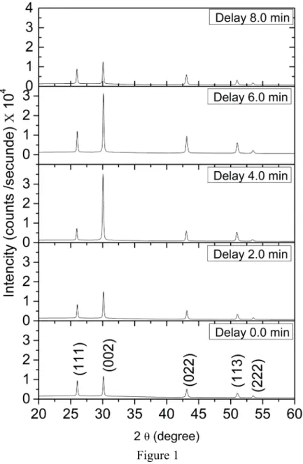
Fig.1 shows that all films have a cubic crystal structure. When the delay time was four and six minutes, the peak intensities of the films were higher than that of the other films. Although the film thicknesses were the same, the high peak intensity indicated that crystallization was good for these films. Previous studies had demonstrated a strong correlation between the rate of reaction and the quality of crystallization[4].
The texture coefficient given in Eq. 6 [13]was used to calculate the preferred orientation of the films.
𝑇𝑇𝑇𝑇 =𝐼𝐼(ℎ𝑘𝑘𝑘𝑘)/𝐼𝐼0(ℎ𝑘𝑘𝑘𝑘) 1
𝑁𝑁∑ (𝑁𝑁 𝐼𝐼0(ℎ𝑘𝑘𝑘𝑘)𝐼𝐼(ℎ𝑘𝑘𝑘𝑘))
(6)
In this equation, I0(hkl) wasthe standard intensity of the plane (hkl) given in the ASTM card (98-003-8293), and I(hkl) wasthe measured relative intensity of the plane (hkl). The texture coefficients are given in Table 2. According to Table 2, the preferred orientation was shifted to the (002) plane. Specifically, the TC of the film obtained in DT4 was 2.156. This study showed that the preferred orientation depended on the delay time of adding thiourea to the solution.
The lattices constant calculated from the XRD results that aregiven in Table 3 where it can be seen that the lattice constant of the films isnearly the same as that of the bulk sample. But, the lattice parameter of the film obtained in DT4 is slightly bigger than that of the other films. Differences in texture coefficient values may have caused this situation. The corrected values of lattice constants were estimated from the Nelson–Riley formula given in Eq.7 [14].
𝐹𝐹(𝜃𝜃)= 12�𝑐𝑐𝑐𝑐𝑐𝑐
2𝜃𝜃
𝑐𝑐𝑠𝑠𝑠𝑠𝜃𝜃 + 𝑐𝑐𝑐𝑐𝑐𝑐2𝜃𝜃
𝜃𝜃 � (7)
The Nelson and Riley plots aregiven in Fig. 2 and corrected lattice constant are given in Table 3.(𝑐𝑐𝑐𝑐𝑐𝑐2𝜃𝜃/2) ∗ ( 1
𝑐𝑐𝑠𝑠𝑠𝑠𝜃𝜃+ 1
𝜃𝜃) = 0give the corrected lattice constant. According to the Nelson
Riley plots, the lattice constant of the films obtained in DT4, DT6, and DT8 were higher than the lattice constant of the bulk sample. These values of corrected lattice indicated the films were under strain.
Williamson Hall equation (W-H) is given inEq.8.
𝛽𝛽𝑐𝑐𝑐𝑐𝑐𝑐𝜃𝜃 =𝐾𝐾𝑐𝑐𝑐𝑐λ+ 4𝜀𝜀𝑐𝑐𝜀𝜀𝜀𝜀𝜃𝜃 (8)
Where Kis shape factor of 0.94, ε is a microstrain, λ is wavelength of X-ray radiation (1.54056 Å). For Williamson Hall plots, sinθ along the x-axis and βcosθ along the y-axis are given in Figure 3. From the linear fit to the data, the crystalline size was estimated from the y-intercept[15]. Crystallite size estimated from the W-H plots is given in Table 3.Dislocation density values were calculated according to the W-H plots.
To calculate dislocation density, the crystallite size was used as shown in Eq.9[16]
𝛿𝛿 =(𝑐𝑐𝑐𝑐)12 (9)
When the delay time was 0, the dislocation density of the film was almost that half of the other samples. This result showed that the crystallite size was reduced depending on the time of the addition of thiourea.
2.2 SEM Analysis of PbSFilms
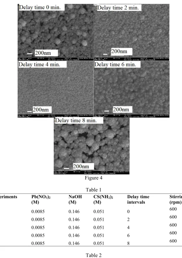
SEM images were used to analyze surface morphology, and these images are given in Fig.4. SEM images were magnified to 30000 times to see the grains. When thiourea was added directly to the final solution, it was noticed that there were many voids on the surface of the sample. This result showed that the surface of the films produced at low temperatures was not completely coated. When the delay time was increased to two minutes, it was seen that the voids on the film surface were relatively reduced. When thiourea was added at four-minute intervals, it appeared that the film surface was completely covered with PbS, and the surface was very compact. In addition, it was clear that there were no pinholes, voids, orcracks on the surface of this film. When the delay time was increased to six minutes, the voids reappeared on the film surface. Finally, when the delay time was increased to eight minutes, the voids on the surface of the film were found to be as many as in the first film. Previous studies[17,18]have suggested that the reaction rate directly affected the quality of the film such as crystallization and compact structure. This study proved that it was possible to produce compact and well-crystallized samples at low temperatures.
Conclusions
In this study, the PbS thin films were produced by the CBD method. As a new approach, thiourea was divided into 10 equal portions and was added to the final solutions at certain time intervals. The effects of this application on the quality of the produced PbS thin films were investigated. In the laboratory conditions where the experiment was carried out, the temperature of the solution was measured as about 15 degrees. The solution was not heated because raising the temperature of the solution to 25 degrees would result in quantitative losses. However, the XRD peak intensity of the film produced by the conventional method at this temperature was relatively low. It is mean that when the thicknesses are same, low XRD peak point to relatively poor crystallization. In addition, the voids on the surface of this film were quite numerous. Thiourea was added to the solution periodically to resolve this problem. It was found that the XRD peak intensity
of the film produced with a delay time of four minutes was higher than the other films produced although all samples had nearly the same thicknesses. This result indicated that the film obtained as DT4 had good crystallization. The surface morphology of the produced films was analyzed by using SEM images. According to the SEM images, when the delay time was four minutes, the surface of the film was quite compact, and there were no voids or pinholes.
List of Figure and Table Captions
Figure 1. X-ray diffraction patterns of PbS films.
Figure 2. Nelson-Riley plots for a) DT0, b) DT2, c) DT4, d) DT6, e)DT8. Figure 3.Williamson-Hall plotsfor a) DT0, b) DT2, c) DT4, d) DT6, e) DT8. Figure 4. Scanning electron microscopy images of PbS films.
Table 1. Experimental details.
Table 2. Texture coefficient of PbS films. Table 3. Structural properties of the PbS films.
Figure 4 Table 1
Table 2 Experiments Pb(NO3)2
(M) NaOH (M) CS(NH(M) 2)2 Delay time intervals ( i ) Stirring (rpm) DT0 0.0085 0.146 0.051 0 600 DT2 0.0085 0.146 0.051 2 600 DT4 0.0085 0.146 0.051 4 600 DT6 0.0085 0.146 0.051 6 600 DT8 0.0085 0.146 0.051 8 600 Experiments DT0 DT2 DT4 DT6 DT8 T.C.(111) 1.003 0.788 0.375 0.629 0.904 T.C.(002) 1.126 1.481 2.156 1.703 1.279 T.C.(022) 0.732 0.729 0.468 0.666 0.816
Table 3
References
[1] R. Bai, D. Kumar, S. Chaudhary, D.K. Pandya, Highly crystalline p-PbS thin films with tunable optical and hole transport parameters by chemical bath deposition, Acta Mater. 131 (2017) 11–21. https://doi.org/10.1016/j.actamat.2017.03.062.
[2] D. Kumar, G. Agarwal, B. Tripathi, D. Vyas, V. Kulshrestha, Characterization of PbS nanoparticles synthesized by chemical bath deposition, J. Alloys Compd. 484 (2009) 463– 466. https://doi.org/10.1016/j.jallcom.2009.04.127.
[3] S. Seghaier, N. Kamoun, R. Brini, A.B. Amara, Structural and optical properties of PbS thin films deposited by chemical bath deposition, Mater. Chem. Phys. 97 (2006) 71–80. https://doi.org/10.1016/j.matchemphys.2005.07.061.
[4] B. Altıokka, Effects of Inhibitor on PbS Thin Films Obtained by Chemical Bath Deposition, Arab. J. Sci. Eng. 40 (2015). https://doi.org/10.1007/s13369-015-1680-3.
[5] B. Abdallah, R. Hussein, N. Al-Kafri, W. Zetoun, PbS Thin Films Prepared by Chemical Bath Deposition: Effects of Concentration on the Morphology, Structure and Optical Properties, Iran. J. Sci. Technol. Trans. A Sci. 43 (2019) 1371–1380. https://doi.org/10.1007/s40995-019-00698-1.
[6] E. Barrios-Salgado, Y. Rodríguez-Lazcano, J.P. Pérez-Orozco, J. Colin, P. Altuzar, J. Campos, D. Quesada, Effect of Deposition Time on the Optoelectronics Properties of PbS Thin Films Obtained by Microwave-Assisted Chemical Bath Deposition, Adv. Condens. Matter Phys. 2019 (2019). https://doi.org/10.1155/2019/5960587.
[7] S. V. Bhatt, M.P. Deshpande, B.H. Soni, N. Garg, S.H. Chaki, Chemical bath deposition of lead sulphide (PbS) thin film and their characterization, Solid State Phenom. 209 (2014) 111–115. https://doi.org/10.4028/www.scientific.net/SSP.209.111.
[8] S. Saravana Kumaran, T. Parveen Banu, Investigation on structural and optical properties of chemically deposited Pbs thin films, Int. J. Recent Sci. Res. 4 (2013) 1685–1687.
[9] M.M. Abbas, A. Ab-M. Shehab, A.K. Al-Samuraee, N.A. Hassan, Effect of deposition time on the optical characteristics of chemically deposited nanostructure PBS thin films, Energy Procedia. 6 (2011) 241–250. https://doi.org/10.1016/j.egypro.2011.05.028.
[10] B. Abdallah, A. Ismail, H. Kashoua, W. Zetoun, Effects of Deposition Time on the Morphology, Structure, and Optical Properties of PbS Thin Films Prepared by Chemical Bath Deposition, J. Nanomater. 2018 (2018) 1–8. https://doi.org/10.1155/2018/1826959. Experiment Crystallite size (nm) From W-H plots Lattice constant for bulk sample (Å) Lattice constant from Nelson-Riley plots(Å) Dislocation density (lines/m2)*1014
from crystallite size
DT0 140 5.936 5.937 0.510
DT2 92 5.936 5.935 1.181
DT4 87 5.936 5.953 1.321
DT6 85 5.936 5.939 1.384
[11] P.E. Bortamuly, G. Chetri, S. Borah, M.N. Bordoloi, Structural and optical properties of ZnS thin films prepared by chemical bath deposition method, Int. J. ChemTech Res. 8 (2015) 396–402. https://doi.org/10.1063/1.4917962.
[12] F. Göde, S. Ünlü, Synthesis and characterization of CdS window layers for PbS thin film solar cells, Mater. Sci. Semicond. Process. 90 (2019) 92–100. https://doi.org/10.1016/j.mssp.2018.10.011.
[13] H. Soetedjo, B. Siswanto, I. Aziz, S. Sudjatmoko, J. Babarsari, Low Resistivity Of Cu And Fe Doped Pbs Thin Films Prepared Using Dc Sputtering Technique, J. Non-Oxide Glas. 9 (2017) 55–63.
[14] N. Choudhury, B.K. Sarma, Structural characterization of lead sulfide thin films by means of X-ray line profile analysis, Bull. Mater. Sci. 32 (2009) 43–47. https://doi.org/10.1007/s12034-009-0007-y.
[15] V. Mote, Y. Purushotham, B. Dole, Williamson-Hall analysis in estimation of lattice strain in nanometer-sized ZnO particles, J. Theor. Appl. Phys. 6 (2012) 2–9. https://doi.org/10.1186/2251-7235-6-6.
[16] A.N. Fouda, M. Marzook, H.M. Abd El-Khalek, S. Ahmed, E.A. Eid, A.B. El Basaty, Structural and Optical Characterization of Chemically Deposited PbS Thin Films, Silicon. 9 (2017) 809–816. https://doi.org/10.1007/s12633-015-9399-z.
[17] B. Altıokka, M.C. Baykul, M.R. Altıokka, Some physical effects of reaction rate on PbS thin films obtained by chemical bath deposition, J. Cryst. Growth. 384 (2013) 50–54.
[18] B. Altıokka, Effects of Inhibitor on PbS Thin Films Obtained by Chemical Bath Deposition, Arab. J. Sci. Eng. 40 (2015) 2085–2093. https://doi.org/10.1007/s13369-015-1680-3.