1. Introduction
Nanowires are promising candidates for future nanoscale electronic devices. Silicon nanowires can be grown using the vapor–liquid–solid method [1], and prototype devices have included bipolar [2] and field-effect transistors [3], solar cells [4], sensors [5], and nonvolatile memories [6]. This diversity of applications has motivated numerous theoretical studies, for instance on the electronic structure of bare and passivated nanowires [7], dopants [8, 9], and transport [10]. An excellent overview of the experimental and theoretical state of the art can be found in the review by Rurali [11].
Most of the applications require doping, and the under-standing of the behavior of dopants in nanowires is still incom-plete. The present paper addresses the electronic structure
of doped hydrogen-passivated Si nanowires as a function of dopant concentration and type of dopants. We focus on B as an acceptor and P as a donor dopant, both widely used to dope Si.
A key characteristic of dopant impurities is their deep or shallow nature. In general it is very difficult to known a priori if an atomic defect will be shallow or deep. Comparison with the same defect in different materials, combined with a knowl-edge of the absolute location of the valence and conduction band can give some indication. For example, it was found that hydrogen-related defect levels line up in a wide variety of mat-erials [12]. The standard theoretical approach to examine this explicitly in the case of dopants in bulk semiconductors is by considering the different possible charge states as function of the possible Fermi levels [13]. For a donor, the relevant charge states are positive and neutral (all of our discussions apply equally well to acceptors, mutatis mutandis). If the trans ition
Journal of Physics: Condensed Matter
Ab initio study of hydrogenic effective mass
impurities in Si nanowires
H Peelaers1,2,6, E Durgun3,4, B Partoens2, D I Bilc3,5, Ph Ghosez3,
C G Van de Walle1 and F M Peeters2
1 Materials Department, University of California, Santa Barbara, CA 93106-5050, United States of America 2 Departement Fysica, Universiteit Antwerpen, Groenenborgerlaan 171, B-2020 Antwerpen, Belgium 3 Theoretical Materials Physics Quantum Materials Center, CESAM Research Unit, Université de Liège (B5), B-4000 Liège, Belgium
4 UNAM-National Nanotechnology Research Center and Institute of Materials Science and Nanotechnology, Bilkent University, Ankara 06800, Turkey
5 Molecular and Biomolecular Physics Department, National Institute for Research and Development of Isotopic and Molecular Technologies, RO-400293 Cluj-Napoca, Romania
E-mail: [email protected]
Received 27 July 2016, revised 23 December 2016 Accepted for publication 6 January 2017
Published 27 January 2017 Abstract
The effect of B and P dopants on the band structure of Si nanowires is studied using electronic structure calculations based on density functional theory. At low concentrations a dispersionless band is formed, clearly distinguishable from the valence and conduction bands. Although this band is evidently induced by the dopant impurity, it turns out to have purely Si character. These results can be rigorously analyzed in the framework of effective mass theory. In the process we resolve some common misconceptions about the physics of hydrogenic shallow impurities, which can be more clearly elucidated in the case of nanowires than would be possible for bulk Si. We also show the importance of correctly describing the effect of dielectric confinement, which is not included in traditional electronic structure calculations, by comparing the obtained results with those of G0W0 calculations.
Keywords: si nanowires, shallow impurities, confinement effects, first-principles calculations (Some figures may appear in colour only in the online journal)
H Peelaers et al
Ab initio study of hydrogenic effective mass impurities in Si nanowires
Printed in the UK 095303 JCOMEL
© 2017 IOP Publishing Ltd 29
J. Phys.: Condens. Matter
CM
10.1088/1361-648X/aa5768
Paper
9
Journal of Physics: Condensed Matter IOP
2017
1361-648X
6 Author to whom any correspondence should be addressed.
doi:10.1088/1361-648X/aa5768
from the positive to the neutral charge state occurs for Fermi levels above the conduction-band minimum (CBM), the donor is ‘shallow’. In that case, the neutral charge state (in which the electron would be bound tightly to the impurity center) is not stable and the electron is transferred to the conduction band. Of course, at sufficiently low temper ature the electron can still be bound to the positively charged ionized donor center, also called a ‘hydrogenic effective mass’ state [14], but this state consists almost entirely of host wave functions, as is evident from the description in effective mass theory [14]. The actual impurity state of a shallow donor (with a wave function local-ized on the impurity itself) is well above the CBM, i.e. a reso-nance in the conduction band, and therefore difficult to identify either computationally or experimentally.
Computational studies of doped nanostructures typi-cally do not address the distinction between the hydrogenic effective mass state and the actual impurity state, leading to much confusion. Misleading language, such as ‘impurity band’ or ‘defect level’ (e.g. for Si nanowires [15–17]), and figures depicting band structures of doped nanostructures (e.g. [17–23]) seemingly showing an ‘impurity band’, contribute to this confusion. While these examples are for Si nanowires, this confusion also occurs for other doped lower-dimensional systems. In this paper we address this common misconception explicitly, using the example of doped Si nanowires and with state-of-the-art electronic structure methods.
Effective mass theory (EMT) provides an intuitive pic-ture for the binding of electrons to shallow donors, showing a series of hydrogenic states below the band edge. However, EMT itself describes the states only in terms of proper-ties of the host (effective mass and dielectric constant) and cannot distinguish between different donor impurities. If a more accurate description of the shallow state is required, for instance to predict the ionization energies associated with dif-ferent dopant impurities, more sophisticated techniques have to be employed. Density functional theory (DFT) in prin-ciple provides such information, but in practice the extended states associated with shallow dopants cannot be adequately described within the volume of computationally tractable supercells, e.g. a tight-binding study of P in bulk Si showed that cells with 125 000 atoms were required to encompass the extended states and to converge the binding energy [24].
However, in low-dimensional systems such as nanowires, there are two effects, occurring simultaneously, that can make the extended states more localized: quantum confinement and dielectric confinement. Quantum confinement (due to the con-fining potential of the surrounding vacuum region) is correctly accounted for in all DFT calculations. Dielectric confinement, which in a macroscopic picture is caused by the mismatch of the dielectric constant inside and outside the nanowire, gives rise to image polarization charges on the surface. In a microscopic picture a similar effect should be contained in the exchange-correlation potential of DFT. This effect increases band gaps and can localize extended states [25–27]. Dielectric confinement is present even in nanowires with larger diameters (e.g. >20 nm) for which the effect of quantum confinement is negligible, and has been observed experimentally [28] in these large diameter nanowires. Conventional DFT functionals, such
as the local density approximation (LDA) and the generalized gradient approximation (GGA), do not describe this effect; hybrid functionals are expected to capture it partially [29]. Many-body perturbation theory (such as the G0W0 approach),
on the other hand, is capable of fully describing dielectric confinement. A tight-binding approach that included both di electric and quantum confinement [27] observed an increase in the ionization energy of P impurities with decreasing diam-eter of Si nanowires. Nanowires are therefore a good test system to reveal the EMT behavior of shallow impurities.
In this paper we will focus on atomic shallow impuri-ties, which can be described by EMT, and where the actual impurity state is in the conduction band for donors and in the valence band for acceptors. In case the actual impurity state, with the wave function localized on the defect, occurs in the band gap (e.g. as happens in N/B doped Si nanoribbons [23]), the impurity is not shallow, but deep. Low-dimensional sys-tems can also be doped by the physisorption or chemisorption of molecules on the surface [30], which can lead to different behavior that is not the subject of this paper.
2. Methodology
Here we use state-of-the art DFT and G0W0 calculations to
elucidate the behavior of P and B dopants in Si nanowires. Our DFT calculations are performed using projector aug-mented-wave pseudopotentials [31] with a plane-wave basis, as implemented in the vasp code [32]. A plane-wave cutoff of 255 eV and a 1× ×1 20 k-point grid for the smallest unit cell (and equivalent k-point sampling for the larger unit cells) was used. All cells were fully relaxed so that the forces are smaller than 5 meV A˚−1 and the stress smaller than 50 meV A˚−3.
In a study focused on band structure it is important to use a DFT functional that accurately describes the electronic struc-ture and is not subject to the band-gap error associated with conventional (semi-)local functionals. We therefore used the HSE06 [33, 34] hybrid functional which mixes in 25% of Hartree–Fock exact exchange; this produces a band gap for bulk Si of 1.16 eV. The results reported here do not depend on the choice of hybrid functional, as we checked explicitly with the crystal code [35] by also employing the B1-WC hybrid functional [36, 37], which mixes the generalized gradient approximation of Wu and Cohen [38] with 16% of Hartree–Fock exact exchange within the B1 scheme [39]. In each case, the atomic structure was fully relaxed at the hybrid functional level.
Our G0W0 calculations used the abinit code [40, 41]. A
Coulomb potential cutoff [42] was applied to remove the spu-rious long-range Coulomb interaction between the periodic images, so that convergence with respect to the cell size and
k-point grid can be achieved. An extrapolar scheme [43] was used to aid in the convergence with respect to the number of bands included. To obtain the dielectric function we used a
1× ×1 30 (1× ×1 14 for the largest supercell) q-point sam-pling and a total number of empty bands equal to 10 times the number of occupied bands. More details about the techniques and the convergence can be found elsewhere [44].
3. Results and discussion
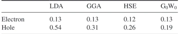
We will focus here on a (1 1 0)-oriented hydrogenated Si nanowire with a diameter d = 1.2 nm (see figure 1 for a cross section and side view). (1 1 0) is the preferred growth direc-tion observed in experiments for d <10 nm [45]. Since the value of the electron and hole effective mass of the undoped nanowire plays an important role in EMT, e.g. it determines the effective Bohr radius of the EMT state, we list the calcu-lated electron and hole effective masses obtained using dif-ferent functionals in table 1. The electron effective masses are very similar for the different functionals, but the hole effective masses strongly depend on the functional.
For our doping studies we place the dopant as shown in figure 1(a), at the near-edge position that was previously found to be preferred [18]. Different dopant concentrations are modeled by changing the length of the supercell in the growth direction. The different cases are labeled by n, the number of Si unit cells per dopant atom (each with length 3.84 Å) included along the wire direction of a 1× ×1 n supercell (figure 1(b)).
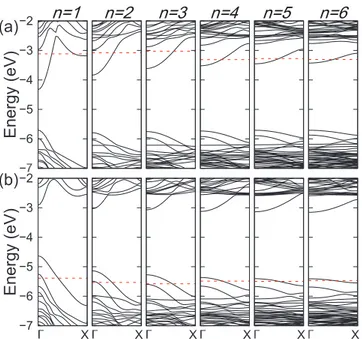
The band structures for P-doped and B-doped wires obtained with HSE06 are shown in figure 2. The vacuum level was chosen as common zero energy level, enabling the align-ment of the different band structures. Figure 2(a) shows that as the concentration of the dopant is decreased, the lowest con-duction band in the P-doped case becomes separated from the other bands. Similar considerations apply to the valence band in the B-doped case (figure 2(b)). Note that with increasing n, folding of the Si bands occurs, as the corresponding Brillouin zone becomes n-times smaller. The x-axis scale used for the band structures is based on the reciprocal lattice vector, so that despite the decreasing Brillouin zone, the width of the plots remains the same.
The bands around the indicated Fermi levels (horizontal lines) in figure 2 show increasingly less dispersion as n increases, and it is tempting to associate them with the P and B impurity levels. A closer examination is necessary, however. In figure 3 we compare the band structure of a P- or B-doped nanowire (n = 6) with that of an undoped nanowire, calcu-lated in the same-size supercell so that zone-folding effects
are comparable. The comparison shows that the lowest duction band, which appears separated from the other con-duction bands in figure 3(b) for the P dopant case, is already present in the undoped nanowire. It results from folding of the bulk CBM near the X point. This lowest conduction band is clearly not an impurity level, but is actually part of the Si host band structure. The smaller n, the larger the perturbation of this band due to the impurity, leading to larger deviations from a pure Si band.
The presence of the dopant does cause some modifications. Degeneracies at the edge of the Brillouin zone are lifted due to the breaking of the symmetry, but that happens in the valence band as well as the conduction band. What is physically rel-evant is that the dispersion of the lowest conduction band is reduced in the presence of P doping, and its Fermi level is shifted to lower energy. For a neutral P atom, this lowest conduction band is occupied with one electron and thus half filled. In the dilute limit, this band would become truly flat, corresponding to the hydrogenic effective-mass state. Note that in this case the upper valence bands are also perturbed by the presence of the P dopant, but inspection of the corre-sponding wave functions shows that these states are nanowire states. This can also be seen from the projected density of states (PDOS), shown in figure 4(a), where the valence bands do not contain any significant P character. Similar behavior is observed in the B-doped nanowire (figure 3(c) and PDOS in figure 4(b)).
This PDOS also confirms that in the case of P doping the lowest conduction bands indeed have almost exclusively Si character, while P character only shows up at much higher energies (analysis of the wave functions at Γ shows P-centered states starting from 0.79 eV above the CBM, which is con-sistent with the PDOS of figure 4(a)). Identifying the lowest
Figure 1. (a) Cross section of a P-doped hydrogen-passivated Si nanowire with a diameter of 1.2 nm. (b) Side view, indicating the Si unit cell along (1 1 0), and boundaries of the 1× ×1 n supercell, where n = 1, 2, or 3.
Table 1. Electron and hole effective masses of a 1.2 nm (1 1 0)-oriented hydrogenated nanowire, obtained using different functionals. The results for LDA and G0W0 are taken from [44].
LDA GGA HSE G0W0
Electron 0.13 0.13 0.12 0.13
conduction band as an ‘impurity band’ is therefore clearly not correct. This lowest state is a level with predominantly sil-icon character, only slightly perturbed by the presence of the dopant, completely in accord with the concepts of hydrogenic effective mass theory [14]. The same can be observed for B doping, where the highest valence band has predominantly Si character. States with more B character start at 0.65 eV below the VBM, as indicated by the PDOS shown in figure 4(b) and confirmed by wave function analysis.
We can now further quantify the shallow dopants by cal-culating the ionization energy, which is the energy required to ionize the dopant (or equivalently, the energy required by the bound hole or electron to become unbound). From our
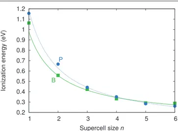
calculations we can extract a value for this ionization energy for P (B), by comparing the absolute positions of the bottom (top) of the impurity-induced band with the absolute position of the CBM (or valence-band maximum, for B) of the undoped wire. Figure 5 shows the value of the ionization energy as a function of supercell size, along with fits of the data, taking only the n = 3, 4, 5, and 6 data points, to the empirical form ula Eion=E∞ion+a n/ , where a is a fitting parameter. An extrapolation to large n allows us to estimate the value in the dilute limit (E∞ion), which for the P-doped wire is 0.07 eV, and for the B-doped wire, 0.13 eV. These values have a significant error bar, as for n = 6 the width of the impurity-induced band is still 0.33 eV for P and 0.14 eV for B. A measure of the error bar can be obtained by comparing the fitting results obtained by using the n = 3, 4, 5, and 6 data points with those obtained only using the n = 4, 5, and 6 data points. This gives an esti-mate of 0.06 eV for B and 0.005 eV for P. The calculations performed with the B1-WC functional yield similar ionization energies, to within 0.02 eV. These HSE06 results indicate that the ionization energy for P in the nanowire is modified only slightly from its value in bulk Si (0.045 eV), while for B the deviation from the bulk value (also 0.045 eV) is significantly larger. A possible explanation is that the B atom, which has a smaller ionic radius compared to Si or P, undergoes a much larger relaxation in the nanowire than in bulk Si. For P this relaxation effect is much smaller [18].
We thus find that the ionization energies of the dopants are modified from their bulk values. Comparing explicitly for P in our 1.2 nm nanowire, Han et al [15] reported an ionization energy of ∼0.16 eV based on DFT using LDA, but using a dif-ferent procedure to extract the ionization energy. Rurali et al
Figure 2. HSE06 band structures for (a) P-doped and (b) B-doped 1.2 nm Si nanowires as a function of the dopant concentration. Each supercell contains one dopant atom, and from left to right the size of the supercell (1× ×1 n) is increased by increasing n from 1 to 6, corresponding to decreasing dopant concentrations. The horizontal dashed line indicates the calculated Fermi level.
Figure 3. HSE06 band structures of (a) undoped, (b) P-doped, and (c) B-doped Si nanowires, all calculated using an n = 6 supercell. The red line indicates the calculated Fermi level.
Figure 4. Projected density of states of (a) the P-doped, and (b) the B-doped n = 6 nanowire. The vertical dotted line indicates the Fermi level. The dashed black line is the total DOS, while the dotted red and solid blue (green) lines indicate the Si and P (B) contributions to the DOS. The Si PDOS shown is the total PDOS of all Si atoms. The H contributions are not shown. The insets show a breakdown of the PDOS of each impurity-induced band as a percentage of the total DOS.
[46] found 0.93 eV using a hybrid functional for a comparable sized nanowire, but with a different (center) location of P.
As mentioned before, dielectric confinement is inade-quately described by DFT; the hybrid functional partially cap-tures the effect since it includes a fraction of exact exchange. Niquet et al [29] suggested that the fraction of the interac-tion captured by the hybrid funcinterac-tional would correspond to the percent age of exact exchange included in the func-tional, which is 25% in our case. Figure 6 shows the results obtained from this extrapolation based on the fraction of exact exchange; it leads to an ionization energy of 0.25 eV for P and 0.37 eV for B. The earlier LDA results [15] do not include any of this effect, while the hybrid functional of Rurali et al [46] included a fraction (12%) of the effect. Diarra et al [27] used a different approach: they employed tight binding and included the di electric confinement based on macroscopic electrostatics. They found an ionization energy of 1.25 eV, but (as acknowledged by Diarra et al) the electrostatic approach may not be valid for small-diameter nanowires.
We therefore performed G0W0 calculations, which include
the full effect of the dielectric confinement. This allows us to explicitly test the accuracy of the scheme based on extrapola-tion of the fracextrapola-tion of exact exchange, and also to check the accuracy of the tight-binding + macroscopic electrostatics approach. We performed the G0W0 calculations for n = 2,
n = 3, and n = 4 P-doped nanowires. The results are shown in figure 6, along with a fit that leads to an ionization energy of 0.61 eV in the dilute limit. These results show that the dielectric confinement effect is indeed important, and not fully captured by the hybrid functional calculations. The ‘HSE06 + extrapo-lation’ approach yielded a value of 0.25 eV, significantly underestimating the full result. On the other hand, our G0W0
result is much smaller than the tight-binding result [27] of 1.25 eV, indicating that macroscopic electrostatics does not adequately describe small-diameter nanowires.
4. Conclusion
In summary, we performed an ab initio study of the nature of B and P dopants in Si nanowires. In the process, we were able to elucidate fundamental mechanisms that are less easily examined in bulk, and that have frequently been misunder-stood in previous work. The introduction of a dopant causes a band to appear near the valence- or conduction-band edge, but this state is not strongly localized on the impurity; rather, it corresponds to the shallow-dopant-induced hydrogenic state familiar from effective mass theory. We also showed the importance of dielectric confinement in low-dimensional systems: G0W0 calculations capture this effect, while hybrid
functionals (even with extrapolation) or macroscopic electro-static approaches provide a poor description.
Acknowledgments
This work was supported by the Flemish Science Foundation (FWO-Vl), the NSF MRSEC Program under award No. DMR11-21053, and the Army Research Office (W911NF-13-1-0380). DIB acknowledges financial support from the grant of the Romanian National Authority for Scientific Research, CNCS UEFISCDI, project No. PN-II-RU-TE-2011-3-0085. Ph G acknowledges a research professorship of the Francqui foundation and financial support of the ARC project AIMED and FNRS project HiT4FiT. This research used resources of the Céci HPC Center funded by F R S-FNRS (Grant No. 2.5020.1) and of the National Energy Research Scientific Computing Center, a DOE Office of Science User Facility supported by the Office of Science of the US Department of Energy under Contract No. DE-AC02-05CH11231.
References
[1] Schmidt V, Wittemann J V, Senz S and Gösele U 2009
Adv. Mater.21 2681–702
[2] Cui Y and Lieber C M 2001 Science 291 851–3
[3] Thelander C, Agarwal P, Brongersma S, Eymery J, Feiner L, Forchel A, Scheffler M, Riess W, Ohlsson B, Gösele U and Samuelson L 2006 Mater. Today 9 28–35
Figure 5. Ionization energies calculated with HSE06 for P and B in 1.2 nm nanowires as a function of dopant separation. The lines are fits, as explained in the text.
Figure 6. Ionization energies calculated for P in 1.2 nm nanowires as a function of dopant separation, using HSE06 and using an extrapolated HSE06 value to include the dielectric confinement effect. The lines are fits, as explained in the text. Also shown are the full G0W0 results.
[4] Tian B, Kempa T J and Lieber C M 2009 Chem. Soc. Rev. 38 16–24
[5] Tian B, Cohen-Karni T, Qing Q, Duan X, Xie P and Lieber C M 2010 Science 329 830–4
[6] Duan X, Huang Y and Lieber C M 2002 Nano Lett. 2 487–90
[7] Ng M F, Zhou L, Yang S W, Sim L Y, Tan V B C and Wu P 2007 Phys. Rev. B 76 155435
[8] Rurali R, Palummo M and Cartoixà X 2010 Phys. Rev. B 81 235304
[9] Peelaers H, Partoens B and Peeters F M 2009 Nano Lett. 9 107–11
[10] Markussen T, Rurali R, Cartoixà X, Jauho A P and Brandbyge M 2010 Phys. Rev. B 81 125307
[11] Rurali R 2010 Rev. Mod. Phys. 82 427–49
[12] Van de Walle C G and Neugebauer J 2003 Nature 423 626–8
[13] Freysoldt C, Grabowski B, Hickel T, Neugebauer J, Kresse G, Janotti A and Van de Walle C G 2014 Rev. Mod. Phys. 86 253–305
[14] Luttinger J M and Kohn W 1955 Phys. Rev. 98 915
[15] Han J, Chan T L and Chelikowsky J R 2010 Phys. Rev. B 82 153413
[16] Chan T L, Zhang S B and Chelikowsky J R 2011 Appl. Phys.
Lett.98 133116
[17] Durgun E, Akman N, Ataca C and Ciraci S 2007 Phys. Rev. B 76 245323
[18] Peelaers H, Partoens B and Peeters F M 2006 Nano Lett. 6 2781–4
[19] Fernandez-Serra M V, Adessi C and Blase X 2006 Phys. Rev.
Lett96 166805
[20] Moon C Y, Lee W J and Chang K J 2008 Nano Lett. 8 3086–91
[21] Leao C R, Fazzio A and da Silva A J R 2008 Nano Lett. 8 1866–71
[22] Durgun E, Akman N and Ciraci S 2008 Phys. Rev. B 78 195116
[23] Zheng F B, Zhang C W, Yan S S and Li F 2013 J. Mater.
Chem. C 1 2735
[24] Martins A S, Boykin T B, Klimeck G and Koiller B 2005
Phys. Rev. B 72 193204
[25] Muljarov E A, Zhukov E A, Dneprovskii V S and Masumoto Y 2000 Phys. Rev. B 62 7420–32
[26] Niquet Y M, Lherbier A, Quang N H, Fernández-Serra M V, Blase X and Delerue C 2006 Phys. Rev. B 73 165319
[27] Diarra M, Niquet Y M, Delerue C and Allan G 2007
Phys. Rev. B 75 045301
[28] Björk M T, Schmid H, Knoch J, Riel H and Riess W 2009
Nat. Nanotechnol.4 103–7
[29] Niquet Y M, Genovese L, Delerue C and Deutsch T 2010
Phys. Rev. B 81 161301
[30] Paulla K K and Farajian A A 2013 J. Phys. Chem. C 117 12815–25
[31] Blöchl P E 1994 Phys. Rev. B 50 17953
[32] Kresse G and Furthmüller J 1996 Phys. Rev. B 54 11169–86
[33] Heyd J, Scuseria G E and Ernzerhof M 2003 J. Chem. Phys. 118 8207
[34] Heyd J, Scuseria G E and Ernzerhof M 2006 J. Chem. Phys. 124 219906
[35] Dovesi R, Orlando R, Civalleri B, Roetti C, Saunders V R and Zicovich-Wilson C M 2005 Z. Kristallogr. 220 571–3
[36] Bilc D I, Orlando R, Shaltaf R, Rignanese G M, Íñiguez J and Ghosez P 2008 Phys. Rev. B 77 165107
[37] Durgun E, Bilc D I, Ciraci S and Ghosez P 2012 J. Phys.
Chem. C 116 15713
[38] Wu Z and Cohen R E 2006 Phys. Rev. B 73 235116
[39] Becke A D 1996 J. Chem. Phys 104 1040–6
[40] Gonze X et al 2005 Z. Kristallogr. 220 558–62
[41] Gonze X, Amadon B, Anglade P M, Beuken J M, Bottin F, Boulanger P, Bruneval F, Caliste D, Caracas R and Côté M 2009 Comput. Phys. Commun. 180 2582–615
[42] Ismail-Beigi S 2006 Phys. Rev. B 73 233103
[43] Bruneval F and Gonze X 2008 Phys. Rev. B 78 085125
[44] Peelaers H, Partoens B, Giantomassi M, Rangel T, Goossens E, Rignanese G M, Gonze X and Peeters F M 2011 Phys. Rev. B 83 045306
[45] Wu Y, Cui Y, Huynh L, Barrelet C J, Bell D C and Lieber C M 2004 Nano Lett. 4 433–6
[46] Rurali R, Aradi B, Frauenheim T and Gali A 2009 Phys. Rev. B 79 115303