[7]
Defect Luminescence in Some Layered Binary
Chalcogenide Semiconductors
A.Aydinli1 and N.M.Gasan|y2
1 Physics Department, Bilkent University, Ankara 06533, Turkey
2Physics Department, Middle East Technical University, Ankara 06531, Turkey
Keywords: Chalcogenides, Defects, Layered Semiconductors, Optical Properties
Abstract. A number of semiconductors such as GaS, GaSe, GaSSe show layered structure where intralayer bonding is strong and interlayer bonding quite weak. With bandgaps mostly in the visible and the near infrared and high crystal structure anisotropy, such semiconductors olfer interesting possibilities for optoelectronic applications In this review, we will summarize the recent developments on the photoluminescent properties of these materials such as luminescence due to donor-acceptor pair recombination. As these materials are undoped, the observed photoluminescence is attributed mostly to defect states present in these materials.
Inroduction
Layered semiconductors have attracted much attention due to their structural properties and possible
optical applications [1]. Elements of the group III-VI allow for a number of binary and ternary
compounds such as GaS, GaSe, TlInSz, GaSexSI.x that crystallize in a layered structure. The layered structure contains a number of alternating layers whose number within the unit cell can be more than one. A good example is GaS where each layer is composed of four atoms stacked along the c axis of a hexagonal structure with a repeating unit of S-Ga-Ga—S and there are two layers in the unit cell [2]. GaS crystallizes in the so called ,B—polytype and carries the symmetry properties of the D2,, space group. Intralayer forces are primarily ionic-covalent, while the interlayer interactions are dominated by van der Waals forces. Due to weak interlayer interaction these materials are easily cleaved along these layers. Likewise, GaSe crystallizes in a hexagonal structure [3] however, depending on the stacking sequences exhibit four modifications labeled; 8, B, y, and 6-polytypes. The e and B are 2H hexagonal type while y and 6 are 3R trigonal type. The 3prevalence of a particular polytype is a fimction of growth techniques. Solid solutions of A —B6X-C61.x have typically been observed to display layered structures with the polytype of the binary parent compound dominating that of the mixed crystal for values of x close to that of the binary compound . Mixed polytypes have also been observed for a narrow range of x values For example, in the case of GaSe1.x, polytype a has been observed for x<0.01, a mixture of polytypes e and y for 0.0l<x<0.03, polytgype y for 0.05<x<0.4 and polytype B for O.5<x<1, [2]. Finally, ternary compounds of the A3B C62 type in which binary parents A3C6 and BSC6 have the ratio of 1:1 also display layered structures [4].
Energy band structures of these layered semiconductors show both indirect and direct band gaps [1,5] mostly in the visible and the near infrared. Much work has been done with near band edge emission in both binary and ternary mixed crystals identifying both direct and indirect, free and bound excitonic states [6-11]. Particularly notable is the observation of resonant exciton in GaSe [12] where the free exciton associated with the direct band gap and states near the indirect conduction band minimum are involved. Free and bound excitons have also been observed both in mixed crystals [13,14] and in ternary compounds of A3B6C62 type. [15,16]. In cases where the samples are not intentionally doped both direct and indirect bound excitons can be attributed to
All rights reserved. No part of contents of this paper may be reproduced or transmitted in an form or b an mea 'th tth ' ' '
excitons bound to residual defects present due to nonostoichometry or less than perfect growth conditions [17].
Recombination luminescence from lower lying states has been observed and attributed to impurities and defects as well as band to band recombination. Numerous studies of photoluminescence in GaSe with impurity levels such as Li [18], Cu [19], Mn[20,2l], Cr[22], Zn [23], Cd [24], Ag [25] and even Tm [26] have been conducted to name a few. Impurity levels in other binary III-VI chalcogenides such as InSe [27,28] have also been studied using
photoluminescence techniques.
While much can be learned from near band edge emission of
semiconductors, recombination luminescence from states lower in energy (i.e: deep level photoluminescence) can also be very informative in the information it provides about impurity levels and defect states [29]. Typically, both the temperature and excitation intensity dependence of the PL peak energies, linewidths and intensities are analyzed to identify the nature of the transitions involved in the recombination processes. In this paper, we will review the recent work done in deep level photoluminescence characterization of some layered binary semiconductors. As the crystals used in this work are not intentionally doped, recombination transitions involving impurity states are thought to originate from either unintentional impurities or point or line defects due to incomplete stochiometry or problems associated with growth conditions. Ternary and quaternary layered chalcogenide semiconductors are beyond the scope of this work.A. GaS. GaS is a binary chalcogenide, similar to GaSe and InSe. It has two layers in a unit cell with each layer consisting of four atoms stacked along the c axis with a repeating unit of S-Ga-Ga-S. GaS crystallizes in the B-polytype. GaS has a wide bandgap that is indirect and has a value of 2.59 eV at 300 K [30]. A direct band gap also exits at approximately 0.45 eV higher in energy. It is considered to be an important material for possible applications for blue emitting devices. It exhibits both electroluminescence and PL in the green-blue region [31]. Both undoped and Zn doped GaS samples has been studied with photoluminescence [7, 32] and some of the features in the near band edge emission was attributed to recombination of shallow donors with distant acceptors [13]. Deep level luminescence from GaS was also observed [33]. We recently studied the deep level PL emission from GaS [34]. We obtained temperature and excitation intensity dependent PL data from single crystals of undoped GaS. Typical photoluminescence data obtained at 10 K displays three broad peaks centered at 558 nm (2.22 eV) 614 nm (2.02 eV) and 780 nm (1.59 eV) labeled as A-,B-, and C-bands respectively. A plot of the PL intensity of each peak versus 1000/T yields the activation energies, AE, of all three bands by fitting the equation:
[:10 exp(AE/kBT) (q)
where 10 is the incident light intensity and k3 is the Boltzmann’s constant. The activation energies obtained are 0.017, 0.013, 0.151 eV for A-band, B-band and C—band, respectively. The fact that as grown GaS behaves as an n-type semiconductor leads us to consider that the activation energies of 0.017 and 0.013 eV are associated with donor levels. Temperature dependence of the peak energies of the bands are shown in Fig.1. Bands A— and B- decrease with increasing temperature, similar to the temperature dependence of the band gap. On the other hand, the energy of the PL peak of the C-band first increases sharply followed by a monotonic increase up to 130 K followed by a decrease to its value at 10 K. Both the blue and the red shift of the PL peak energy is approximately 120 meV. At higher temperatures, the peak energy of the PL peak shows a small trend to increase once more. The blue shifting of PL peak energies have previously been studied in the framework of
configuration coordinate (CC) model [3 5]. Linewidth analysis of the PL peaks have also been done.
As expected, the linewidths (FWHM) of the PL peaks of A- and B-bands do not show much dispersion with increasing temperature while the linewidth of the C-band shows nonlinearPeak Energy (eV) 2'4 ' I I l | I %AA A 2.2 - A AAA _ AA 2.0 _A‘p‘“A“‘ A A-band _ A B-band o C-band 1.8 — — 00 00°00 0 00 o 16 15300 °°°°°°°°°°oo _ 1_4 . I . I . I . J I 0 50 100 150 200 250 300 Temperature (K)
Fig.1. Temperature dependence of the PL peak energies for bands A—, B-, and C for undoped GaS single crystals.
increase when plotted against square root of the temperature, Fig.2. The discontinuity at 50 K corresponds to the initial blue shift on the C-Band. Dispersion of the linewidth of the C-band
0.4 v 0.3 ~ 0.2 —
FWHM
(eV)
0.1 , ‘ A A‘ A‘ AAA A A A»band
A B-band o, O C-band -—Fit A A A A A AA A A A A A A Fig.2. Temp 1/2 T112 ( K )
erature dependence of the PL linewidths for bands A—, B-, and C for undoped GaS single crystals
has been fitted to linewidth
equation using the CC model where the linewidth, W, is expressed as:
W = We coth(h ve /2kBT)”2
(Eq.2)
Here, W0 is a constant and hve is the energy of the vibrational mode of the excited state. Coupled with the results of the excitation dependence of the PL peak energy and intensity, the model that has
been proposed to explain the nature of the observed bands are as follows: Bands A- and C- are the results of donor-acceptor pair (DAP) recombination. The emission energy from a DAP recombination is given as;
Z Z
E(r):Eg —(E3+Eg)+# (Eq.3)
8r
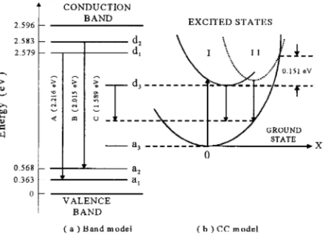
where EE is the band gap energy, E3 and E3 are the ionization energies of the acceptor and the donor, 8 is the dielectric constant, Zn and ZA are the charges of the donor and the acceptor states and r is the distance between the impurities. For A- and B- bands, the observed no shift upon increasing excitation intensity suggested that either only close pairs or homogenous distribution of pairs are involved in the recombination process. C-band is associated with the ground and excited states of the CC model presented in Fig.3. Here the ground and excited states are derived from acceptor and donor levels, respectively. The energy of 150 meV required for thermal quenching, is indicated at the intersection of the ground state with the point at which the second excited state becomes occupied. The origin of these states are thought to be gallium vacancies.
CONDUCTION BAND 2.596 _ EXCITED STATES 2.583 — — d2 2.579 7 d1 _J'__ A “f: 0.151eV > Q S E d; ---0 ND m 0\ >~. 2 Z 3 w c v C 3-; < an o _ ______ __-_.- _ -__ ‘1 GROUND m _ a3 _______ STATE 0 0.568 — a2 0.363 _ 4— al 0 VALENCE BAND
(a)Band model (b)CC model
Fig. 3. Proposed model for the observed PL from GaS.
In their work on GaS grown by iodine transport method, Aono et.al. [36] suggested that,
gallium vacancies with two charged states (V52, V53 ) may be present where V5: is thought to be an
excited state of V5; with the release of an electron. The energy level of V5: is, therefore, higher
than that of V5; . Above model of gallium vacancies does not categorically rule out the existence of other defect states and more data is required before afirm conclusion can be made.B. GaSe. GaSe is perhaps one of the most studied layered chalcogenide semiconductors [13, 37-39]. Capozzi and Montagna [38] have shown that increasing defect concentrations lead} to increasing PL intensity as well as blue shift in the PL peak energy. In the analysis of both excitonic and impurity related emission bands, no impurity specific recombination luminescence was detected
.[37], hence suggesting that donor and acceptor states taking place in the recombination process are derived from structural defects which increase with increasing dopant concentration. Recently, in a detailed analysis of deep level luminescence from e-GaSe two broad bands centered at 644 nm
(1.925 eV) (A—band) and 695 nm (1.784 eV)(B-band) at 10 K were observed [40]. Temperature dependence of PL intensity indicates activation energies of 0.014 eV and 0.076 eV for the shallow
acceptor states involved in the recombination for A- and B—bands, respectively. Similar values to the latter have been observed in various works on undoped e-GaSe [41-43]. Blue shifi of the B-band with excitation intensity is shown in Fig. 4 and follows clearly the expected behavior from donor-acceptor pair luminescence [44];
E —E 3 _
L(E )=L0 Map _3(_1§B_Q (Eq.4)
1’
E, +11, —2E,
E, —E,,
where, L0 is a proportionality constant, E3 is the emitted photon energy of a close donor—acceptor pair separated by a shallow impurity Bohr radius RB and E°° is the emitted photon energy of an infinitely distant donor-acceptor pair. This analysis yields two donor levels: One at 0.264 eV, and the other at 0.163 eV below the bottom of the conduction band. In addition to two acceptor levels at 0.051 eV and 0.152 eV above the valence band maximum, two donor levels at 0.170 and 0.420 eV below the bottom of conduction band were found in [39] and acceptor levels at 0.20 eV and 0.44 eV as well as a donor level at 0.006 eV from their respective band edges were identified in [3 8]. While donor bands identified at 0.170 eV and 0.163 eV are in agreement with those in [40], other levels are different. This may be due to the existence of several donor and acceptor states both deep and shallow in undoped GaSe depending on growth conditions. We suggest that these levels are mostly
likely associated with stacking faults or dislocations which are easy to form in GaSe due to weak
van der Waals forces between the layers.U! A i w I N 1-Excitation Intensity (W cm '2) o I . . . 1 770 1.775 1.730 1,785
Peak Energy ( eV)
Fig. 4. Blue shifi of the PL peak as a function of excitation laser intensity in undoped e-GaSe.
C. GaTe. In contrast with other layered semiconductors, GaTe is one of the less studied materials. This is due to the difficulties in growing GaTe which has a monoclinic crystal structure. In contrast with earlier works on the excitonic PL in GaTe, recent PL studies identified two peaks [45] at 1.76 eV and 1.59 eV at 97 K; one associated with an exciton while the other was a deep level emission. Analysis of the temperature dependence of deep level luminescence band suggests the existence of a donor level at 0.03 eV below the conduction band minimum and an acceptor level 0.15 eV above the top of the valence band. In this work formation of the acceptor level was attributed to defects or defect complexes that may exist in GaTe. Other PL work [46] at 10 K revealed three bands located at 1.781 eV, 1735 eV and 1.575 eV. The high energy band was narrow and was identified as a
direct free exciton while the second highest energy band was attributed to an exciton bound to a
neutral donor. The broad deep level luminescence at 1.575 eV was found to be weakly temperaturedependent and considered as a donor-acceptor pair transition. The proposed transition for this band
involves a donor level at 0.170 eV below the bottom of the conduction band and an acceptor level 0.056 eV above the top of the valence band. The authors in [46] suggests that both surface and bulk dislocations are possible in GaTe and may be involved in the deep level luminescence recombination process without discounting the possibility of unintentional impurities that may have contaminated the samples during growth.
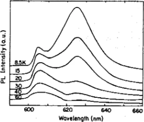
D. InS. 1115 is a layered semiconductor along the lines of GaS, GaSe, and InSe. In the latter crystals, the metal atoms have a tetrahedral coordination of three chalcogene atoms and both types of atoms are located in the same layer. In ms, the same tetrahedral coordination exists, however, in this case two S atoms and an In atom is in the same layer and the third S atom is in the neighboring layer. Therefore, InS has a three dimensional network somewhat different than other layered crystals. InS has an indirect band gap of 2.11 eV and a direct gap 047 eV above it. Three bands centered at 605 nm (2.05 eV, A-band), 626 nm (1.98 eV, B-band) and 820 nm (1.51 eV, C-band) were identified at 10 K [47] and only the first two were analyzed in detail using both temperature and excitation intensity dependence, Fig.5. A donor level at 0.010 eV below the indirect conduction band and an acceptor level at 0.12 eV above the valence band maxiumum are identified as the donor-acceptor pair while a second donor level at 0.06 eV below the indirect conduction band minima is involved in a transition to the valence band maximum.
’3
S
r '5 § 3.5K .5 l5 3‘ 20 3 600 520 540 660 Wavelength (nm)Fig. 5. Temperature dependent photoluminescence spectra of ms. Out of the three PL peaks observed only two peaks were analyzed since the third PL peak shifts beyond the
range of the spectrometer into the infrared.
E. InSe. InSe has a band gap of 1.24 eV and 1.353 eV at room temperature and 1.6 K, respectively and has structure similar to GaS and GaSe. InSe has been studied using near band edge emission [48] and direct free exciton at 1.336 eV and a direct bound exciton at 1.333 eV were observed. Perhaps the richest spectra were obtained in [49] where four peaks at 1.334, 1.306, 1.288. and 1.232 eV were recorded. The first of these peaks were identified as a free exciton recombination while others were attributed to impurity-band, donor—acceptor pair and an impurity-vacancy complex, respectively. Time resolved PL studies of InSe in the range of 123-180 eV [50] also suggest that structural defects are responsible for the observed bands. In [51] the origin of the recombination of two peaks at 1.377 eV and 1.237 eV at 77 K have been identified as free or weakly bound exciton and a donor-acceptor pair transition. It should be noted that in this study, after Hg doping of InSe, deep level luminescence band present in undoped samples increase in intensity suggesting that
luminescence may be originating from same type of centers. The authors make it clear that based
on the layered characteristics of InSe, defects should be present in the form of dislocations and/or
stacking faults. The observed acceptor level at 0.07 eV above the valence band maximum is thought
to be due to a defect or defect complex.Conclusions
The study of deep level luminescence peak energy, intensity and linewidth as a fianction of temperature and excitation laser energy provides a lot of information to identify transitions involved in the recombination processes involved in the photoluminescence of layered chalcogenide semiconductors. Whether the transitions are due to impurity to band, band to band or donor to acceptor transitions can be differentiated using this information. Excitation laser intensity dependence of the PL intensity gives the initial clue [52] on the nature of the transitions. Red shift of the PL peak energy with increasing temperature can indicate, in addition to the shrinkage of the band gap, thermal emission of carriers bound to impurity levels and therefore to increased pair separation [53], hence a red shifi of the observed PL peak energy, through Eq.3. Blue shift of PL peak energy is typically understood within the CC model. Temperature dependence of the linewidth provides fiirther evidence to confirm the identification [44]. There is ample evidence in the literature suggesting the presence of defects in these quasi two—dimensional crystals and in the absence of doping, defects may be responsible for the acceptor and/or donor states. It should be noted that the evidence for the role of defects in the deep level luminescence obtained using PL spectroscopy is indirect and other measurement techniques should be employed to fiirther confirm the PL data. As one goes from binary to ternary and quaternary semiconductors, defect formation through compositional disorder in the crystals is expected to increase. As mentioned in the introduction, literature on such semiconductors is also expanding rapidly.
Acknowledgements
We would like to thank our past and present students K. Goksen, O. Gurlu, l. Yilmaz, and A. Bek for performing most of the experiments in this work.
References
[1] Optical and Electrical Properties of Layered Materials, edited by RA. Lee (Reidel, Dordrecht, 1976).
[2] A.Gouskov, J .Camassel, and L.Gouskov, Prog. Crystal Growth and Charact. Vol.5 (1982), p.323.
[3] A.Kuhn, A.Chevy, and R. Chevalier Phys. Stat. Sol. (a) Vol. 31 (1975), p.469. [4] K.R.Allahkverdiev, T.G.Mamedov, B.G.Akinoglu, and S.S.Ellialtioglu, Tr. J. Physics
Vol.18 (1994), p.1.
[5] M.P.Hanias, AN. Anagnostopoulos, K. Kambas, J. Spyridelis, Mat.Res.Bull. Vol. 27,
(1992), p.25.
[6] A. Cingolani, A. Minafra, P. Tantalo, and C. Paorici, Phys. Stat. Sol.A, Vol. 4 (1972), p. K83.
[7] A. Mercier, E. Mooser, J.P.Voitchovsky, J. Luminescence Vol 7 (1973), p. 241. [8] Ph. Schmid, J.P.Voitchovsky and A. Mercier, Phys. Stat. Sol. A, Vol. 21 (1974), p.443. [9] Yu. P. Gnatenko, Z.D. Kovalyuk, P.A. Skubenko, Yu. I. Zhirko, Phys. Stat. Sol. B, Vol.
117 (1983), p.283.
[10] J. Camassel, P. Merle, H. Mathieu and A. Gouskov, Phys. Rev. B Vol. 19 (1979), p. 1060.
[11] V.Capozzi, Phys. Rev. B, Vol. 23 (1981), p.836.
[12] A. Mercier, E. Mooser, J. P, Voitchovsky, Phys. Rev B. Vol. 12 (1975), p.4307. [13] A.Mercier and J.P.Voitchovsky, J. Phys. Chem. Solids, Vol. 36 (1975), p.1411. [14] N. Kuroda and Y. Nishina, Phys. Stat. Sol. B, Vol. 72 (1975), p.81.
[15] T. Arai, J. Aoyagi, Y. Maryama, S. Onari, K.R. Allahkverdiev and E. Bairamova, Japan J. Appl. Phys. V0132 (suppl. 3) (1993), p.754.
[16] J.A. Kalomiros and AN. Anagnostopoulos, Phys. Rev. B Vol. 50 (1994), p.7488 [17] Le Chi Thanh and C.Depeursinge, Solid State Commun. Vol. 25 (1978), p.499. [18] S. Shigetomi and T. Ikari, Philosophical Magazine Letters Vol. 79 (1999) p.575. [19] V. Capozzi, Phys. Rev. B Vol, 28 (1983), p.4620.
[20] Yu. P. Gnatenko, Yu. I. Zhirko, P. A. Skubenko , Sov .Phys. Solid State Vol. 30 (1988), p.1540.
[21] 800—11 Lee, Suk-ryong Hahn, Choong-Hyun Chung Sang-Hyun Yun, and Wha-Tek Kim, Solid State Commun. Vol. 60 (1986) p.453.
[22] C.H.Chung, S.R.Hahn, H.L.Park, W.T. Kim S.I.Lee, J. Luminescence, Vol. 4041 (1988), p.405.
[23] S. Shigetomi, T. Ikari, and H. Nakashima, J. Appl. Phys. Vol. 74 (1993), p.4125. [24] S. Shigetomi, T. Ikari, H. Nishimura, J. Appl. Phys. Vol. 69 (1991), p.7936. [25] S. Shigetomi, T. Ikari, H. Nakashima, Phys. Stat. Sol. A, Vol. 160 (1997), p.159. [26] B.G.Tagiev, G.M. Nifiiev and F. Sh. Aidaev, Phys. Stat. Sol. B, Vol. 128 (1985), p.K65. [27] S. Shigetomi, T. Ikari, H. Nakashima, Phys. Stat. Sol. B, Vol. 209 (1998), p.93.
[28] F ,J .Manjon, Y. Van der Vijver, A. Segura, V. Munoz, Z.X. Liu and C. Ulrich, Phys. Stat. Sol. B Vol. 211 (1999), p.105.
[29] P.E.Mozol’, E.A. Sal’kov, N.A. Skubenko, P.A. Skubenko and Z.D. Kovalyuk, Sov.
Phys. Solid State, Vol. 27 (1985), p.2228.
[30] E. Aulich, J.L.Brebner and E. mooser Phys. Stat. Sol. Vol. 31 (1969), p.129.
[31] M.I.Karaman and VP. Mushinskii, Sov.Phys. Semicond. Vol. 3 (1970), p.662.
[32] T.Aono, K.Kase, and A.Kinoshita, J. Appl. Phys. Vol. 74 (1993), p.2818. [33] M.I.Karaman and VP. Mushinskii, Sov.Phys. Semicond. Vol.4 (1970), p.464. [34] A.Aydinli, N.M.Gasanly, K. Goksen, J. Appl. Phys. Vol. 88 (2000), pl. [35] C.C.Klick and J .H. Schulman, Solid State Physics, Ed. F. Seitz and D. Turnbull(Academic, New York, 1957) Vol.5, p.110.
[36] T.Aono, K.Kase, and A. Kinoshita, J. Appl. Phys, Vol. 74 (1993), p.2818 [3 7] J .P.Voitchovsky and A. Mercier, Il Nuovo Cimento, Vol. 22 (1974), p.273. [38] V. Capozzi and M. Montagna, Phys. Rev. B, Vol. 40 (1989), p.3182. [39] V. Capozzi, Phys. Rev. B, Vol. 28 (1983), p.4620.
[40] A.Aydinli, N.M.Gasanly, K. Goksen, Philosophical Magazine Lett., Vol. 81 (2001), p. 859.
[41] C, Tatsuyama, C. Hamaguchi, H. Tomita and J. Nakai, Jap. J. Appl. Phys, Vol. 10
(1971), p.1698.
[42] C. Manfredotti, A. Rizzo, C. De Blasi, S. Galassani and L. Rugierro, J. Appl. Phys, Vol. 46 (1975), p.4531.
[43] FL lsamailov, G.A. Akhundov, OR. Vernich, Phys. Stat. Sol. Vol. 17 (1966), p. K237 .
[44] E. Zacks and A. Halperin, Phys. Rev. B Vol. 6 (1972) , p.3072.[45] S. Shigetomi, T. Ikari, H. Nishimura, J. Lumin. Vol. 78 (1998), p.117.
[46] H.S.G1'ider, B, Abay, H. Efeoglu, Y.K.Yogurtcu, J. Lumin. Vol. 93 (2001), p.243. [47] N.M.Gasanly and A. Aydinli, Solid State Commun. Vol. 101 (1997), p.797. [48] Yu. P. Gnatenko and Yu. I. Zhirko, Phys. Stat. Sol. B, Vol. 142 (1987), p.595. [49] B. Abay, H. Efeoglu, Y. K.Yogurtcu, MRS Bulletin Vol. 33 (1998),p.1401. [50] J .LBrebner, T. Steiner, and M.L.W. Thewalt, Solid State Commun. Vol. 56 (1985),
p.929.
[51] S. Shigetomi, T. Ikari and H. Nakashima, Phys. Stat. Sol. B, Vol.209 (1998), p.93. [52] T. Schmidt, K. Lischka and W. Zulehner, Phys. ReV.B,Vol. 45 (1992), p.8989.
[53] J ,HSchon, O.Schenker, H. Riazi-Nejad, K, Friemelt, Ch. Kloc and E. Bucher, Phys. Stat. Sol. AVol. 161(1997), p.301.