All-aluminum hierarchical plasmonic surfaces in
the infrared
Sencer Ayas,1,3 Gokhan Bakan,1,2,4 and Aykutlu Dana1
1 UNAM Institute of Materials Science and Nanotechnology, Bilkent University, 06800 Ankara, Turkey 2Department of Electrical and Electronics Engineering, Antalya International University, 07190 Antalya, Turkey
3[email protected], 4[email protected]
Abstract: All-Aluminum metal-insulator-metal resonator structures with multiple metal-insulator stacks showing resonances in the mid-infrared (MIR) are fabricated. Ultrathin native Al2O3 is used as the insulator layers enabling simple fabrication of the resonator structures. The structures with two oxide layers exhibit two distinct resonances in the MIR. Simulation of these structures shows confinement of magnetic field to the thicker bottom oxide at the shorter wavelength resonance and to the thinner top oxide at the other resonance. Simulations of higher order hierarchical structures with 3 and 4 oxide layers show multispectral response with precise control of the oxide thicknesses. The studied structures show great potential for IR applications that require durability and multispectral characteristics.
©2016 Optical Society of America
OCIS codes: (160.3918) Metamaterials; (240.6680) Surface plasmons; (260.5740) Resonance; (230.4555) Coupled resonators.
References and links
1. T. Xu, A. Agrawal, M. Abashin, K. J. Chau, and H. J. Lezec, “All-angle negative refraction and active flat lensing of ultraviolet light,” Nature 497(7450), 470–474 (2013).
2. A. Moreau, C. Ciracì, J. J. Mock, R. T. Hill, Q. Wang, B. J. Wiley, A. Chilkoti, and D. R. Smith, “Controlled-reflectance surfaces with film-coupled colloidal nanoantennas,” Nature 492(7427), 86–89 (2012).
3. S. Xiao, V. P. Drachev, A. V. Kildishev, X. Ni, U. K. Chettiar, H.-K. Yuan, and V. M. Shalaev, “Loss-free and active optical negative-index metamaterials,” Nature 466(7307), 735–738 (2010).
4. A. S. Roberts, A. Pors, O. Albrektsen, and S. I. Bozhevolnyi, “Subwavelength plasmonic color printing protected for ambient use,” Nano Lett. 14(2), 783–787 (2014).
5. K. Aydin, V. E. Ferry, R. M. Briggs, and H. A. Atwater, “Broadband polarization-independent resonant light absorption using ultrathin plasmonic super absorbers,” Nat. Commun. 2, 517 (2011).
6. Z. H. Jiang, S. Yun, F. Toor, D. H. Werner, and T. S. Mayer, “Conformal dual-band near-perfectly absorbing mid-infrared metamaterial coating,” ACS Nano 5(6), 4641–4647 (2011).
7. X. Liu, T. Tyler, T. Starr, A. F. Starr, N. M. Jokerst, and W. J. Padilla, “Taming the Blackbody with Infrared Metamaterials as Selective Thermal Emitters,” Phys. Rev. Lett. 107(4), 045901 (2011).
8. N. Liu, M. Mesch, T. Weiss, M. Hentschel, and H. Giessen, “Infrared perfect absorber and its application as plasmonic sensor,” Nano Lett. 10(7), 2342–2348 (2010).
9. X. Liu, T. Starr, A. F. Starr, and W. J. Padilla, “Infrared spatial and frequency selective metamaterial with near-unity absorbance,” Phys. Rev. Lett. 104(20), 207403 (2010).
10. S. Ayas, G. Cinar, A. D. Ozkan, Z. Soran, O. Ekiz, D. Kocaay, A. Tomak, P. Toren, Y. Kaya, I. Tunc, H. Zareie, T. Tekinay, A. B. Tekinay, M. O. Guler, and A. Dana, “Label-free nanometer-resolution imaging of biological architectures through surface enhanced Raman scattering,” Sci. Rep. 3, 2624 (2013).
11. D. Wang, W. Zhu, M. D. Best, J. P. Camden, and K. B. Crozier, “Wafer-scale metasurface for total power absorption, local field enhancement and single molecule Raman spectroscopy,” Sci. Rep. 3, 2867 (2013). 12. A. Polman and H. A. Atwater, “Photonic design principles for ultrahigh-efficiency photovoltaics,” Nat. Mater.
11(3), 174–177 (2012).
13. H. A. Atwater and A. Polman, “Plasmonics for improved photovoltaic devices,” Nat. Mater. 9(3), 205–213 (2010).
14. M. W. Knight, H. Sobhani, P. Nordlander, and N. J. Halas, “Photodetection with active optical antennas,” Science 332(6030), 702–704 (2011).
15. A. A. Yanik, A. E. Cetin, M. Huang, A. Artar, S. H. Mousavi, A. Khanikaev, J. H. Connor, G. Shvets, and H. Altug, “Seeing protein monolayers with naked eye through plasmonic Fano resonances,” Proc. Natl. Acad. Sci. U.S.A. 108(29), 11784–11789 (2011).
16. N. Liu, M. L. Tang, M. Hentschel, H. Giessen, and A. P. Alivisatos, “Nanoantenna-enhanced gas sensing in a single tailored nanofocus,” Nat. Mater. 10(8), 631–636 (2011).
17. A. Tittl, P. Mai, R. Taubert, D. Dregely, N. Liu, and H. Giessen, “Palladium-based plasmonic perfect absorber in the visible wavelength range and its application to hydrogen sensing,” Nano Lett. 11(10), 4366–4369 (2011). 18. E. Cubukcu, S. Zhang, Y.-S. Park, G. Bartal, and X. Zhang, “Split ring resonator sensors for infrared detection of
single molecular monolayers,” Appl. Phys. Lett. 95(4), 043113 (2009).
19. R. Adato, A. A. Yanik, J. J. Amsden, D. L. Kaplan, F. G. Omenetto, M. K. Hong, S. Erramilli, and H. Altug, “Ultra-sensitive vibrational spectroscopy of protein monolayers with plasmonic nanoantenna arrays,” Proc. Natl. Acad. Sci. U.S.A. 106(46), 19227–19232 (2009).
20. R. Adato and H. Altug, “In-situ ultra-sensitive infrared absorption spectroscopy of biomolecule interactions in real time with plasmonic nanoantennas,” Nat. Commun. 4, 2154 (2013).
21. C. Koechlin, P. Bouchon, F. Pardo, J. Jaeck, X. Lafosse, J.-L. Pelouard, and R. Haïdar, “Total routing and absorption of photons in dual color plasmonic antennas,” Appl. Phys. Lett. 99(24), 241104 (2011). 22. S. J. Tan, L. Zhang, D. Zhu, X. M. Goh, Y. M. Wang, K. Kumar, C.-W. Qiu, and J. K. W. Yang, “Plasmonic
color palettes for photorealistic printing with aluminum nanostructures,” Nano Lett. 14(7), 4023–4029 (2014). 23. M. K. Hedayati, M. Javaherirahim, B. Mozooni, R. Abdelaziz, A. Tavassolizadeh, V. S. K. Chakravadhanula, V.
Zaporojtchenko, T. Strunkus, F. Faupel, and M. Elbahri, “Design of a perfect black absorber at visible frequencies using plasmonic metamaterials,” Adv. Mater. 23(45), 5410–5414 (2011).
24. J. A. Dionne, E. Verhagen, A. Polman, and H. A. Atwater, “Are negative index materials achievable with surface plasmon waveguides? A case study of three plasmonic geometries,” Opt. Express 16(23), 19001–19017 (2008). 25. J. A. Dionne, L. A. Sweatlock, M. T. Sheldon, A. P. Alivisatos, and H. A. Atwater, “Silicon-Based Plasmonics
for On-Chip Photonics,” IEEE J. Sel. Top. Quantum Electron. 16(1), 295–306 (2010).
26. W. Lee, S. Y. Lee, R. M. Briber, and O. Rabin, “Self-Assembled SERS Substrates with Tunable Surface Plasmon Resonances,” Adv. Funct. Mater. 21(18), 3424–3429 (2011).
27. Y. Chu, M. G. Banaee, and K. B. Crozier, “Double-resonance plasmon substrates for surface-enhanced Raman scattering with enhancement at excitation and stokes frequencies,” ACS Nano 4(5), 2804–2810 (2010). 28. C. D’Andrea, J. Bochterle, A. Toma, C. Huck, F. Neubrech, E. Messina, B. Fazio, O. M. Maragò, E. Di Fabrizio,
M. Lamy de La Chapelle, P. G. Gucciardi, and A. Pucci, “Optical Nanoantennas for Multiband Surface-Enhanced Infrared and Raman Spectroscopy,” ACS Nano 7(4), 3522–3531 (2013).
29. L. V. Brown, K. Zhao, N. King, H. Sobhani, P. Nordlander, and N. J. Halas, “Surface-enhanced infrared absorption using individual cross antennas tailored to chemical moieties,” J. Am. Chem. Soc. 135(9), 3688–3695 (2013).
30. J. Le Perchec, Y. Desieres, N. Rochat, and R. Espiau de Lamaestre, “Subwavelength optical absorber with an integrated photon sorter,” Appl. Phys. Lett. 100(11), 113305 (2012).
31. P. Bouchon, C. Koechlin, F. Pardo, R. Haïdar, and J.-L. Pelouard, “Wideband omnidirectional infrared absorber with a patchwork of plasmonic nanoantennas,” Opt. Lett. 37(6), 1038–1040 (2012).
32. C. M. Watts, X. Liu, and W. J. Padilla, “Metamaterial electromagnetic wave absorbers,” Adv. Mater. 24(23), OP98–OP120, OP181 (2012).
33. G. V. Naik, V. M. Shalaev, and A. Boltasseva, “Alternative plasmonic materials: beyond gold and silver,” Adv. Mater. 25(24), 3264–3294 (2013).
34. G. V. Naik, J. Liu, A. V. Kildishev, V. M. Shalaev, and A. Boltasseva, “Demonstration of Al:ZnO as a plasmonic component for near-infrared metamaterials,” Proc. Natl. Acad. Sci. U.S.A. 109(23), 8834–8838 (2012).
35. S. Law, L. Yu, A. Rosenberg, and D. Wasserman, “All-semiconductor plasmonic nanoantennas for infrared sensing,” Nano Lett. 13(9), 4569–4574 (2013).
36. G. Garcia, R. Buonsanti, E. L. Runnerstrom, R. J. Mendelsberg, A. Llordes, A. Anders, T. J. Richardson, and D. J. Milliron, “Dynamically modulating the surface plasmon resonance of doped semiconductor nanocrystals,” Nano Lett. 11(10), 4415–4420 (2011).
37. M. Kanehara, H. Koike, T. Yoshinaga, and T. Teranishi, “Indium tin oxide nanoparticles with compositionally tunable surface plasmon resonance frequencies in the near-IR region,” J. Am. Chem. Soc. 131(49), 17736–17737 (2009).
38. J. M. Luther, P. K. Jain, T. Ewers, and A. P. Alivisatos, “Localized surface plasmon resonances arising from free carriers in doped quantum dots,” Nat. Mater. 10(5), 361–366 (2011).
39. M. W. Knight, N. S. King, L. Liu, H. O. Everitt, P. Nordlander, and N. J. Halas, “Aluminum for plasmonics,” ACS Nano 8(1), 834–840 (2014).
40. G. H. Chan, J. Zhao, G. C. Schatz, and R. P. Van Duyne, “Localized surface plasmon resonance spectroscopy of triangular aluminum nanoparticles,” J. Phys. Chem. C 112(36), 13958–13963 (2008).
41. G. Maidecchi, G. Gonella, R. Proietti Zaccaria, R. Moroni, L. Anghinolfi, A. Giglia, S. Nannarone, L. Mattera, H.-L. Dai, M. Canepa, and F. Bisio, “Deep ultraviolet plasmon resonance in aluminum nanoparticle arrays,” ACS Nano 7(7), 5834–5841 (2013).
42. J. Martin, J. Proust, D. Gérard, and J. Plain, “Localized surface plasmon resonances in the ultraviolet from large scale nanostructured aluminum films,” Opt. Mater. Express 3(7), 954 (2013).
43. J. Olson, A. Manjavacas, L. Liu, W.-S. Chang, B. Foerster, N. S. King, M. W. Knight, P. Nordlander, N. J. Halas, and S. Link, “Vivid, full-color aluminum plasmonic pixels,” Proc. Natl. Acad. Sci. U.S.A. 111(40), 14348–14353 (2014).
44. A. Ono, M. Kikawada, R. Akimoto, W. Inami, and Y. Kawata, “Fluorescence enhancement with deep-ultraviolet surface plasmon excitation,” Opt. Express 21(15), 17447–17453 (2013).
45. S. Ayas, A. E. Topal, A. Cupallari, H. Güner, G. Bakan, and A. Dana, “Exploiting Native Al 2 O 3 for Multispectral Aluminum Plasmonics,” ACS Photonics 1(12), 1313–1321 (2014).
46. P. Jouy, Y. Todorov, A. Vasanelli, R. Colombelli, I. Sagnes, and C. Sirtori, “Coupling of a surface plasmon with localized subwavelength microcavity modes,” Appl. Phys. Lett. 98(2), 021105 (2011).
1. Introduction
Metal-Insulator-Metal (MIM) structures with sub-wavelength dimensions can be engineered to exhibit tailored optical properties. Owing to advances in bottom-up and top-down fabrication techniques, such resonator structures continue to attract attention of fundamental and applied research [1–5]. Commonly, MIMs are realized by patterning multiple metal-insulator stacks over a substrate. The structures are typically fabricated using electron beam (e-beam), focus-ion beam and optical lithography which exhibit resonances in the visible and infrared wavelengths [6–9]. Although, typically top down methods are used for fabrication of MIM surfaces, large area surfaces can be achieved using nanoparticles as the top metal layer [2,10,11]. Surfaces that consist of periodic plasmonic structures can be used to tailor absorption of light for photovoltaic [12–14], sensing [15–17], spectroscopy [18–20], color printing [4, 21–23] and waveguide [24,25] applications. Multispectral characteristic of a plasmonic surface is generally accompanied by high field enhancements at the resonance wavelengths that enable the simultaneous use of these surfaces for various applications such as surface enhanced Raman (SERS) [26,27] and surface enhanced infrared absorption (SEIRA) [28,29] spectroscopies. Likewise, MIM based plasmonic structures exhibit multispectral responses that have resonances ranging from the ultraviolet (UV) to mid-Infrared (MIR) wavelengths where the resonance frequency of a mode is simply an integer multiple of the fundamental (1st) mode
(
)
1
n n
ω ≅ ω [30–32]. Although noble metals, such as Au and Ag are most common metals used in fabrication of plasmonic surfaces, there is a growing interest for better performing materials for plasmonic and metamaterial applications in the NIR and MIR wavelengths [33,34]. Transparent conducting oxides and doped semiconductors are widely studied in the IR regime to overcome the challenges that plasmonic metals face [35–38]. Aluminum emerges as the best plasmonic material for applications in the UV, however it is typically not preferred for applications in the near IR due to its interband transition around 800nm and high losses in the IR [39–42]. On the other hand, CMOS compatibility makes Al a good candidate for detector, waveguide, optical interconnects and integrated photonic applications in the IR wavelengths. Aluminum is one of the cheapest and most abundant metals in the world, hence can be used for large scale or disposable nanophotonics applications. Moreover, thin native aluminum oxide (Al2O3) layer protects Al from degradation and makes it favorable for applications such as color printing, which requires durability [22,43]. Recently the effect of the native Al2O3 layer on the optical properties of Al plasmonic structures has been investigated [39,41,42,44,45]. Here, we study all-aluminum broadband hierarchical (multi-layer) plasmonic surfaces consisting of multiple Al and native Al2O3 layers. The hierarchical plasmonic surfaces are simply fabricated by sequential deposition and oxidation of Al films through breaking the vacuum of the physical vapor deposition system to expose the Al films to air. The fabricated hierarchical structures show either multi-spectral or strong single resonance response depending upon the number and thicknesses of native oxide layers as shown by FTIR measurements and FDTD simulations. The implemented method possesses the simplicity of fabrication process for surfaces using native Al2O3 with improved optical response. These structures have potential for applications that require durability, multispectral characteristics such as surface enhanced spectroscopies, optical waveguides, color printing and thermal emitters.
2. Results and discussion
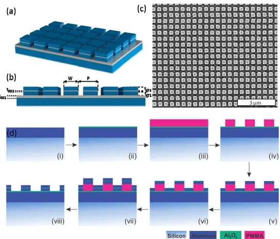
The 3D schematics and top-down scanning electron microscopy (SEM) images of the fabricated hierarchical structures are shown in Fig. 1. The top layer of these structures is designed to have arrays of squares with widths around 300 nm and a period of 500 nm along both x- and y-axis. The thickness of each top Al layer is chosen as 50 nm. Typically the fabrication of such structures requires deposition of multiple dielectric and metal layers. Using Al eliminates the deposition of dielectric layers through the formation the native Al2O3. The thickness of the oxide layer depends on the exposure time of the Al surface to air. Since the native Al2O3 is ultrathin, even small changes in its thickness result in large shifts in the resonance wavelengths of the fabricated structures.
Fig. 1. (a) 3D and (b) side view of the hierarchical aluminum surfaces. Top Al layer thicknesses (tgr1 and tgr2) are 50 nm. The thicknesses of the bottom and top oxide layers are
denoted as tox1 and tox2, respectively. (c) Top-down SEM image of the fabricated structures. (d)
Fabrication of hierarchical Al structures. (i) Deposition of 80 nm thick Al. (ii) Formation of native Al2O3 after exposure of the Al films to air. (iii) PMMA coating. (iv) Pattering PMMA
with e-beam lithography. (v) Deposition of the 1st 50 nm thick Al. (vi) Formation of the 2nd
native Al2O3 layer after vacuum break. (vii) Deposition of the 2nd 50 nm thick Al layer. (viii)
Lift-off process.
The hierarchical Al surfaces are fabricated using e-beam lithography and multiple Al deposition steps. The fabrication steps are shown in Fig. 1c and summarized here. First, silicon substrates are coated with 80 nm thick Al using thermal evaporation following deposition of a thin layer of germanium (5 nm) adhesion layer. The Ge layer also helps achieving smoother Al films as confirmed by AFM measurements. The depositions are performed at 2x10⁻⁶ Torr with a rate of 2-3 Å/s. The rms roughness of the resulting film is
measured as 3 nm. The first Al layer grows a thin Al2O3 layer when exposed to air. Then the samples are spin-coated with 250 nm PMMA for e-beam lithography. Once the PMMA is patterned, 50 nm thick Al is deposited. This first Al layer is exposed to air to form the second native oxide layer by breaking vacuum of the deposition chamber. Then the final Al layer is deposited and the final structures are formed using lift-off process. The area of the fabricated surfaces is 50 μm x 50 μm. The thicknesses of the top and bottom oxide layers are expected to be different. A Thermo K-Alpha monochromated high-performance X-ray photoelectron spectroscopy (XPS) system is used to characterize the thickness of the native Al2O3 layers.
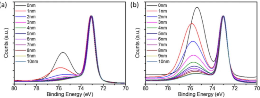
Fig. 2. Depth dependent XPS characterization of Al surfaces with thin native Al2O3 on top. (a)
Just after the deposition of Al films. (b) After the fabrication of hierarchical Al structures.
Depth dependent x-ray photoelectron energy spectra of the fabricated Al surfaces are shown in Fig. 2. The depth dependent binding energy spectrum is obtained by etching the surfaces with ion gun and measuring the energy of the emitted photoelectrons from the etched surface. To characterize the thickness of the top oxide layer, the depth dependent binding energy spectrum for a thick Al film (80 nm) on a silicon substrate is measured just in an hour after the deposition of the film (Fig. 2(a)). The high energy peak corresponds to the aluminum-oxygen binding which indicates the formation of the native Al2O3 film. After 2 nm of etch depth, the high energy peak reduces to 20% of its original intensity value. For 3nm of etch depth, the high energy peak almost disappears. Hence, the thickness of the native Al2O3 on a freshly deposited Al film is deduced to be 2-3 nm. Figure 2(b) shows the depth dependent XPS energy spectra for the Al surfaces outside the patterned area after the fabrication of hierarchical Al structures. The high energy peak is stronger compared to the freshly deposited Al films. After 5 nm of etching, the high energy peak reduces more than 80% and it only slightly changes for further etching. Hence, it is concluded that the thickness of the native Al2O3 on the Al films experienced the fabrication steps is about 5 nm or more. The thicker native oxide on the bottom Al films is expected to be due to longer exposure to air and the chemical processes during the fabrication. The use of acetone, isopropanol alcohol and water might also affect the final thickness of the films.
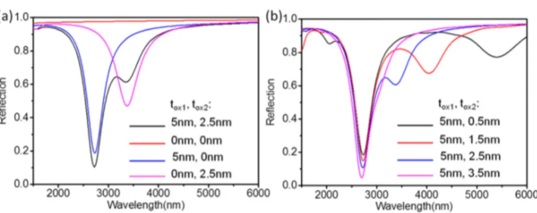
The reflection spectra of the hierarchical Al structures are characterized using Fourier transform infrared spectrometer (FTIR) equipped with a 15x Cassegrain objective in the MIR regime. Since the area of the fabricated hierarchical Al surfaces is 50 μm x 50 μm a knife edge aperture is used to collect light reflected from the patterned area. As the reference sample, an 80 nm thick Al coated silicon substrate is used. Owing to two different oxide thicknesses, two distinct MIR resonances are observed (Fig. 3(a)). These resonances red-shift with increasing widths as expected. The structures are simulated using 2.5nm and 5nm thicknesses for the top and bottom oxide layers, respectively, using a commercial FDTD program (from Lumerical) as shown in Fig. 3(b). In the simulations, the mesh sizes are 5 nm x 5 nm x 0.25 nm around the oxide layer and 5 nm x 5 nm x 2.5 nm for the rest of the
geometry. Material parameters are from the program's material database. CRC and Palik dielectric functions are used for Al and Al2O3, respectively. The simulated spectral responses are similar to the experimental results, however the depths of the experimental resonances are weaker. This discrepancy might be partially due to surface roughness of the Al films which is not accounted for in the simulations. The simulated electric and magnetic field distributions are shown in Fig. 3(c) corresponding to the resonances denoted with (i) and (ii) in Fig. 3(b). Since magnetic field is confined to the Al2O3 layers, the resonances are magnetic plasmon modes by its nature. Magnetic fields are confined to the bottom (5 nm) and top (2.5 nm) native Al2O3 layers for short and long wavelength resonances, respectively. The confinement of longer wavelengths to the thinner oxide layer can be intuitively explained by increased effective refractive index with decreasing oxide thickness, accompanied by a red-shift in the resonance wavelength [46] (λr = 2neffW). Here, neff can be calculated using the following
equation tan h( ) 0
2 d
m d d m
k w
k ε +k ε = , where kd,m = (βSPP2 – εd,mk02)1/2 and neff = βSPP/k0. In Fig. 4, the measured resonance wavelengths on top of the MIM model are shown where the thickness of the oxide layer changes from 1 to 6 nm by 0.5 nm steps in the model. The top and bottom oxide thicknesses are estimated to be 1.5-3 nm and 4.5-5 nm, respectively.
Fig. 3. (a) Measured and (b) simulated reflectance spectra for W = 290 nm, 300 nm, 320 nm and 340 nm (Period = 500 nm). (c) Magnetic field intensities for the resonances shown in (b).
The effect of the top and bottom oxide thicknesses on the reflection spectra are further studied by varying these thicknesses in simulations (Fig. 5). The resonance wavelengths shift drastically with sub-nm changes in the ultrathin oxide layers (2-5 nm) as shown in Fig. 4 for W = 300 nm. When both oxide layers are neglected in the simulations, no resonances in the MIR are observed as expected (Fig. 5(a)). If the thinner top oxide is neglected, only the short
wavelength resonance is excited where it is confined to the bottom oxide layer. If the thicker bottom oxide is neglected, only the longer wavelength resonance is excited where the magnetic field is confined to top oxide layer. The effect of the native oxide layer on the longer wavelength resonance is investigated by varying the thickness of the top oxide layer in between 0.5 nm and 3.5 nm for 5 nm thick bottom oxide layer (Fig. 5(b)). As the top oxide thickness decreases, the longer wavelength resonance red-shifts. As this thickness approaches the bottom oxide’s value (5 nm) the resonances start overlapping. As a result, the top and bottom oxide thicknesses have to be different to observe a multispectral response. If the oxide thicknesses are the same, only one mode is excited with stronger confinement of light into both oxide layers.
Fig. 4. The measured and calculated resonance wavelengths using the MIM model. Oxide thickness changes from 1 to 6 nm with 0.5 nm steps in the model.
Fig. 5. Simulated reflection spectra for (a) varying tox-1 and tox-2, (b) varying tox-2 with
tox-1 = 5 nm. W = 300 nm, P = 500 nm for all cases.
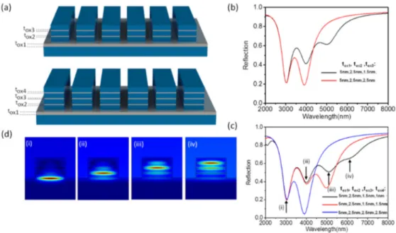
The use of the native oxide as the spacer layer offers an easy fabrication route to re alize higher order hierarchical resonator structures (Fig. 6(a)). The optical response and field distribution of such structures with 3 and 4 oxide layers are studied using simulations. Since the resonance wavelength of an MIM resonator strongly depends on the thickness of the oxide layer, it is possible to excite as many modes as the number of oxide layers. Hence 3 distinct resonances are observed when 3 oxide layers with different thicknesses are used (Fig. 6(b)). Similar to the previous simulation results with two oxide layers, when top two oxide thicknesses are chosen to be the same, only two resonances are observed. The study is repeated for 4 oxide layers and 3 different thickness combinations: 1) all the thicknesses are different, 2) two of the thicknesses are the same, 3) three of the thicknesses are the same resulting in 4, 3 and 2 distinct resonances, respectively (Fig. 6(c) and 6(d)). As the number of
layers with the same thickness increases, the bandwidth decreases, while light couples into the MIM mode determined by the common oxide thickness more strongly.
Fig. 6. (a) 3D schematics of higher order hierarchical aluminum surfaces with multiple MIM resonators. Simulated reflectance spectra for structures with (b) 3, (c) 4 oxide layers. (d) Corresponding magnetic field profiles for the resonances shown in (c). The thickness of the top Al layers is 50 nm, W = 300 nm and P = 500 nm for both geometries.
3. Conclusion
In conclusion, we have demonstrated the utilization of Al and its native oxide for the realization of plasmonics surfaces with multiple resonances in the MIR regime. The use of native oxide eliminates the need for depositing a spacer layer enabling simple fabrication of the hierarchical MIM structures. The structures with two oxide layers exhibit two distinct resonances owing to different thicknesses of the top and bottom oxide layers. The simulations of these structures show confinement of magnetic field into the oxide layers. Simulations of higher order hierarchical structures with 3 and 4 oxide layers show multispectral response when oxide thicknesses are different, and stronger coupling of light when 2 or more oxide layers have the same thickness. These results pave the way for simple fabrication of durable, wide-band plasmonic absorbers for IR applications by precisely controlling the native oxide thicknesses.
Acknowledgments