IET Computers & Digital Techniques
Research Article
Power-efficient reliable register file for
aggressive-environment applications
ISSN 1751-8601 Received on 9th April 2018 Revised 1st February 2019 Accepted on 19th March 2019 E-First on 15th April 2019 doi: 10.1049/iet-cdt.2018.5047 www.ietdl.orgIhsen Alouani
1, Hamzeh Ahangari
2, Ozcan Ozturk
2, Smail Niar
31IEMN-DOAE Laboratory, Polytechnic University Hauts-De-France, Famars, France 2CECS Department, Bilkent University, Ankara, Turkey
3LAMIH Laboratory, Polytechnic University Hauts-De-France, Valenciennes, France E-mail: [email protected]
Abstract: In a context of increasing demands for on-board data processing, insuring reliability under reduced power budget is a serious design challenge for embedded system manufacturers. Particularly, embedded processors in aggressive environments need to be designed with error hardening as a primary goal, not an afterthought. As Register File (RF) is a critical element within the processor pipeline, enhancing RF reliability is mandatory to design fault immune computing systems. This study proposes
integer and floating point RF reliability enhancement techniques. Specifically, the authors propose Adjacent Register Hardened
RF, a new RF architecture that exploits the adjacent byte-level narrow-width values for hardening integer registers at runtime. Registers are paired together by special switches referred to as joiners and non-utilised bits of each register are exploited to enhance the reliability of its counterpart register. Moreover, they suggest sacrificing the least significant bits of the Mantissa to enhance the reliability of the floating point critical bits, namely, Exponent and Sign bits. The authors’ results show that with a low power budget compared to state of the art techniques, they achieve better results under both normal and highly aggressive operating conditions.
1 Introduction
As sub-micron technology dimensions sharply decreased to a few nanometres range in commercialised integrated circuits, the sensitivity of electronic circuits increased drastically making embedded microprocessors more vulnerable to soft errors. Hence, designing dependable systems ready for deployment has become a critical task for chip designers. Especially, these systems have to keep operating reliably even with the presence of faults, to sustain the present growth-rate of device-count and clock-frequency with continuously growing reliability issues.
Random variation in the manufacturing process causes more production yield loss and increases the number of instabilities in chip die. Additionally, the sensitivity of chips is also intensified by voltage scaling since Vdd diminishes with feature size. It also decreases by dynamic voltage scaling (DVS), which is a widely used power reduction technique for dense and power-hungry circuits. As supply voltage dwindles, by technology or DVS, noise margin also decreases proportionally. Thereby, undesirable and accidental faults become more frequent.
Protecting the microprocessor's memory and sequential elements are critical because of its direct impact on the system's reliability and data correctness. Cache memory, register file (RF), flip-flops and latches are common sequential parts of microprocessor architecture, each of which requires its own suitable reliability enhancement. Although cache and RF are both based on SRAM memory technology, their prevalent reliability techniques differ, since their characteristics and applications differ. Architecture level error resilience techniques like Error Correcting Codes (ECCs) have been proposed and widely used [1]. The simplest form is the parity check method whose major weakness is its inability to correct the detected errors [2]. Another form of ECC used in memories is the SECDED (single error correction, double errors detection) [3]. The main shortage of the SECDED is its area overhead and the supplementary latency leading to performance loss. This is more pronounced in RFs, where performance is an essential requirement. Therefore, while effective for cache memories, generally ECC is not considered as a reliability solution in RFs since activity rate per address is higher than cache
memories. Moreover, as RF is located in processors’ critical path, preserving its performance is a priority. Registers in the integer and floating-point RF are used to hold source and destination operands for integer and floating-point computations, respectively. The floating-point operations differ from integer operations data-path and therefore a dedicated RF may be accordingly designed in the CPU micro-architecture such as.
Three main observations motivate us to do this work:
• The need for low power-budget, yet highly reliable, microprocessors for aggressive environments is still an open critical issue.
• The importance of RFs in processors’ reliability.
• Although floating point operations are widely used in critical applications, to the best of our knowledge, there are no floating-point-dedicated works that target RF reliability.
We believe that proposing a suitable technique for RF reliability enhancement is a key challenge in reliable computing system design. The main contributions of this paper are summarised as follows:
• We extend our previous work [4] to a new fault tolerant integer RF based on exploiting vacant spaces in adjacent registers. We combine both architectural and circuit techniques to achieve more robustness in RF with reduced overheads, which targets processors in aggressive environments.
• Combining with our integer RF, a new floating point RF reliability enhancement technique is proposed. The idea is to take advantage of the precision tolerance of a range of applications to achieve low overhead protection. To the best of our knowledge, this is the first reliability enhancement technique considering precision-reliability tradeoffs and dedicated to floating point RF.
This paper is organised as follows: Section 2 presents related studies in the field, while Section 3 describes our architecture. Section 4 discusses floating point RF reliability enhancement.
Section 5 gives our experimental results. Finally, conclusion and future work is explained in Section 6.
2 Related work
While our approach applies to any aggressive environment, we give the related work on potential application domains. One such domain that extensively focuses on reliability is space and aerospace. In the late 90 s, the European Space Agency (ESA) released a 32-bit microprocessor for embedded space-flight applications, called ERC32 [5] that is based on the SPARC V7 architecture. Later, ERC32 was followed by four generations of fault-tolerant LEON-FT processors used in several space projects, including the control computers of the International Space Station [6]. In LEON-FT architectures, parity bits are used to detect errors within the RF. In 2011, a reliable multicore processor was developed for NASA space missions [7] where memory is protected through Hamming Code based ECCs. The problem with ECCs is their high power overheads and time penalties.
In addition to ECCs, several RF reliability studies are based on information redundancy techniques. In some works, register duplication is proposed. For example, in [8], using register renaming unit, unused registers are detected and exploited to preserve redundant copies of other registers.
In-Register Duplication (IRD) is proposed in [9] in which, by an opportunistic idea, dummy sign bits of narrow-width register values are replaced with replication of meaningful bits during RF write operation. For a 64-bit RF, based on distribution of length of operands, extracted from benchmarks, registers are divided into three classes. Those by length of <32, between 32 and 34, and >34. For the first two classes which have dummy sign bits, IRD is applied. ALU detects such sign bits and replaces them with meaningful bits of data. Later, in read operation, replicated and original bits are bitwise compared to find a mismatch as an error indication. Additionally, two parity bits are embedded for each half. By means of both error detection mechanisms, similar to a 2D parity system, they added error detection/recovery for narrow width values in RF. Extra circuit for detecting effective length, applying replication and comparison are all collected in the execution stage with ALU. Duplication is done on the output of ALU, whereas communication path from ALU output to RF input is also protected against transient faults. Nevertheless, long operands are not protected by IRD. If applied to 32-bit RF, this disadvantage is more serious, because long operands are frequent.
In [10], the authors propose an extension to previous work, in which long operands in addition to short operands are also protected. In 32-bit RF, for long operands, values are replicated in other unused registers, similar to [8]. For avoiding the negative effect on performance, two stages are added to the pipeline for detecting efficient length first, and later performing sign extension in the read operation.
All of the works mentioned above are architectural level approaches based on information redundancy and explicit comparison operation. The main difference that our work proposes is that we combine a hardening technique with narrow width duplication. In addition to reducing error rates, by judicious replication in two paired registers, we protect long operands. Provided that a long operand is next to a short one, priority is given
to long operand and replication of its more significant bits are done on dummy sign bits of the short operand.
In the context of emerging approximate computing applications, recent works [11] proposed to find a tradeoff between reliability and computing precision. But, to the best of our knowledge, this is the first work that proposes a reliability enhancement technique for both integer and floating point RFs.
3 Integer RF reliability Enhancement through
Adjacent Register Hardening (ARH)
Our approach improves RF reliability by exploiting unused bits of integer numbers in adjacent registers. Although, any non-numeric data type like strings also benefit, our main focus is on integers since it is more effective for them. For any number in a given range of minimum to maximum possible values in 2's complement system, only one single sign bit is sufficient for correct representation of the number. The remaining sign bits are just multiple copies of the same sign bit and are redundant bits. Based on this observation, instead of preserving multiple redundant bits for sign, we suggest to exploit the redundant bits to enhance the reliability of adjacent registers. ARH is very efficient to protect highly critical data within an application using dummy bits of non-critical registers.
This is even more pronounced for integer values with smaller magnitude. That is, they have more dummy bits which consequently provide more resources for the RF's reliability enhancement. Small numbers have less number of bits to be protected too. Considering this fact, a uniform distribution of large and small numbers will be beneficial for this approach. This is expected from a typical application, but the content of registers is unveiled at run time; hence the extent of reliability increase is application dependent. As can be seen from Fig. 1, numbers with one byte effective length represent more than half of the numbers stored in the RF on average for the tested benchmarks.
Our implementation consists of retrieving the data to store, implementing the technical solution to enhance reliability, and performing the different read/write access. Instead of merely high-level architectural solutions, in our approach, we benefit from a fast circuit level technique. As detailed in the next section, unlike redundancy-based approaches, ARH does not need explicit voting, since circuit-level hardening technique is used. By combining architectural and circuit-level techniques, we reach to a highly flexible reliability solution.
Since the system's higher layers like operating system or compiler are oblivious to the existence of a circuit-level mechanism, our approach does not impose any strict requirement on those higher layers. However, if additional system requirements exist, like criticality of a certain data, the compiler can consider this in register allocation. Dynamic run-time register renaming mechanism can also distribute registers in a better way based on effective length. Such improvements will be the next steps in our future work.
3.1 Circuit level reliability enhancement
To achieve adaptive reliability enhancement and cope with registers stored data state, the proposed approach relies on a configurable circuit level technique. In our proposed architecture, adjacent registers of RF are joined together by 7T/14T technique. Generally, each bit can be joined to any number of bits from any register by embedding multiple switches in between. Nevertheless, to avoid excessive area overhead and complexity, we optimise this idea by just allowing each bit to be joined into a single bit of a single specific register. Thus, registers are paired together bit by bit during RF design. For example, reg0-reg1,…, reg30-reg31. The joiner switches are embedded between these registers to join them when needed.
As shown in Fig. 2 left, 7T/14T [12] is a technique proposed to combine two SRAM cells in circuit level to achieve more reliability or better performance dynamically. According to this idea, two memory cells can be joined together upon request to store a single bit of data into two cells. Joining is done by means of
Fig. 1 Percentage of appearance in the 32-bit RF with different effective lengths (in bytes)
activating two transistors which connect the internal nodes of two cells to each other. For biasing towards reliability, just one of the wordline signals is used for read or write operation (it is called dependable mode). On the other hand, to get more performance both wordlines can be used simultaneously (high-performance mode). If neither cases are required, the joiners are not activated (CTRL = ‘L’, if the switches are NMOS), then the proposed structure works normally as two separate conventional 6T SRAM cells.
7T/14T structure has more reliability due to mutual support from two cells. If there is an instability in one cell, the other one provides more resistance against it. Additionally, in high-performance mode, it shows higher high-performance in terms of read operation speed as read current is provided by two cells. It also allows bigger dynamic voltage reduction because of increased static noise margin (SNM). Since in this work a combination of joined and normal bits may exist inside a single register (i.e. some bits are protected, some are not), we only consider the reliability enhancement benefit, not additional voltage reduction nor performance improvement benefits. However, our approach can be extended to exploit such benefits.
JSRAM cell [13] is an extension of the 7T/14T cell to combine four cells in a ring fashion to achieve full immunity against single bit errors by providing an auto-correction mechanism (Fig. 2 right). It is also capable of tolerating multiple bit upsets (MBUs). Since the RF reliability enhancement in our current work is based on a statistical study and is dependent on the stored data within registers, using 7T/14T scheme is more suitable.
3.2 Architecture level organisation
To enhance the RF error resiliency, we take advantage of the reconfigurable aspect of the 7T/14T cell. Instead of relying on ECCs or extra memory space for reliability enhancement, we use an opportunistic approach that exploits unused bits within the stored data. At bit-level, two paired registers may have up to 32 distinct control signals (named CTRL in Fig. 2) for having bit-level granularity to join individual bits separately (each bit to its counterpart bit). However, this granularity level is not suitable due
to its high area overhead. To optimise the reconfiguration circuitry as well as the additional bit cells, we opted for a byte-level width granularity. Accordingly, the idle bytes are used to harden registers against errors.
Considering byte level granularity, a clever one-to-one mapping between bytes of two registers is required to exploit the empty bits efficiently. Dummy sign bits are on the left-hand side (MSB side), while real data bits are on the other side. Thus, the first obvious paradigm of mapping is in a crossed way, byte-0 of one register to byte-3 of the paired register, byte-2 to byte-1 and so on. Faults in more valuable bits of an integer lead to absolute numerical error. Therefore, alternative mappings are also worth to be investigated (Fig. 3).
While the best mapping is application dependent, we extracted the distribution of operand length for our benchmarks as shown in Fig. 1. Operands with lengths one and four bytes are the dominant ones. Then paired registers of length one-one, one-four, and four-four are more frequent. This means byte mapping has to be biased toward protecting one-one and one-four combinations (four-four cannot be protected anyway). Accordingly, combination (a) in Fig. 3 is not a good option, because it cannot protect one-one case. Among the rest, (b) is more preferable because more valuable bytes are protected in the case of one-four combination. Hence, by limiting ourselves to at most four groups of byte-to-byte joiners, we take mapping of Fig. 3b as most efficient one which leads to better RF error resiliency. For a 32-bit RF, four control signals are required for any of the aforementioned mappings.
For example in the case of mapping in Fig. 3b, if ‘ZYXW’ and ‘V’ hexadecimal values are stored in reg-i and reg-i + 1, respectively, dummy sign bits are filled with redundant values as illustrated in Fig. 4 (top). For having easier routing, bytes can be reordered in one of the registers. In Fig. 4: bottom, reg-i + 1 is reordered. But this requires two multiplexers in input and output of RF to reorder during write and recover proper order during read (Fig. 5).
One superiority of our work in comparison with IRD is that, by pairing registers, ARH can protect long operands. For example, in Fig. 4, reg-i takes four bytes and three of these bytes are protected by reg-i + 1 which takes only one byte. However, in IRD, long operands that represent larger integers are not protected.
Below, we describe the mechanism for basic write/read operations.
3.2.1 Write access: The mechanism behind the write operation is
critical to achieve efficiency. During a write operation, only meaningful bytes are written, while dummy sign bits should not be written. Respective bytes in the register are left intact because they may be keeping redundant data of the paired register. This can be
Fig. 2 Left: 7T/14T memory cell with NMOS joiners [12]. Right: JSRAM cell with NMOS joiners [13]
Fig. 3 Some possible combinations for byte mapping
Fig. 4 Top: Three bytes in reg-i are replicated in sign bits of reg_i + 1 using combination b in Fig. 2. Byte V is not replicated. Bottom: routing by byte reordering
satisfied by having byte selectable write enables. Besides this, while those meaningful bytes are being written and if their counterpart bytes are not in use, control signal of joiners is activated. According to the electrical characteristics of 7T/14T cell, if joiner is activated and one of the paired cells is written, the other one is also written. By exploiting this property, redundant data is quickly written at the same time into the redundant byte inside paired register by single write operation.
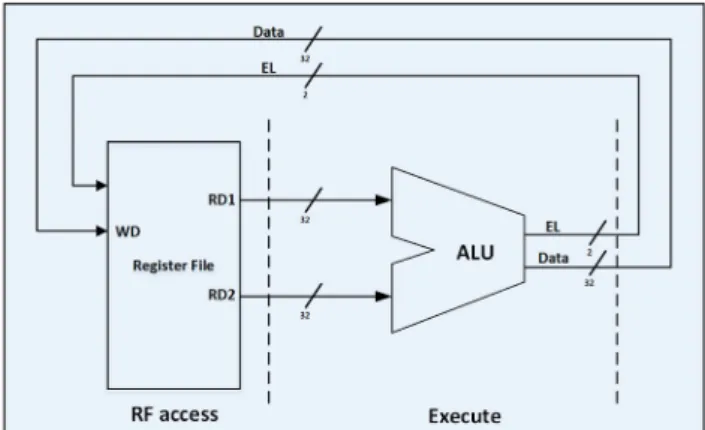
The above-mentioned mechanism requires modification to ALU and RF decoder. As shown in Fig. 6, ALU should simply detect effective length of integer. In addition to storing data within the targeted register address, 2-bit effective length (EL) value is also stored beside the register (Fig. 5). As mentioned earlier, instead of single write enable for each register, here there are four write enable signals, one for each byte. Considering EL value, only necessary byte-selectable write enable signals are activated to write only effective length of data to register. This is shown by AND gates in Fig. 5.
By means of already stored EL of the paired register (of the register being written), unused bytes of paired register are determined to store redundant data. Then proper control signals (for any byte mapping paradigm of Fig. 3) are generated by using two-level AND-OR circuit (Fig. 5).
During the write access, the reliability controller sets the configuration to adapt the available idle bytes to protect the data which is being written. Although the extra circuitry of reliability controller (illustrated in Fig. 5), is on the critical path, by combining it with a decoder during logic synthesis, the delay overhead is minimised. For easier routing for byte mapping, bytes of write data can be reordered for odd or even registers. This operation is in parallel with decoder and is not in the critical path. The reliability controller functionality is explained in the flowchart shown in Fig. 7.
3.2.2 Read access: The read access architecture is modified to
cope with the reliability enhancement process. Once a register's idle byte is exploited for hardening cells, they should be replaced with an actual sign value within the read access to insure data integrity.
As shown in Fig. 5b, the reliability controller selects whether the forwarded data would be the directly read bytes or the sign byte, depending on the register effective width. If the byte-reordering has been already employed in the write operation, original order has to be recovered again. To avoid the timing overhead of detecting sign bit, sign bit can also be stored explicitly like EL values in the write operation, otherwise it is determined by finding MSB bits of most significant byte. This functionality is performed by a multiplexer as depicted in Fig. 5b. This multiplexer selects one of four inputs: directly read byte, reordered byte, all 0/1 for sign extension of positive/negative numbers.
Fig. 5 Read and write access circuits
(a) Write access circuit, wordline and joiner signals, (b) Read access multiplexer
Fig. 6 Simplified datapath for RF write access including EL detection
4 Reliability/precision tradeoff in floating point
RFs
Floating-point arithmetic is an essential ingredient in most of the mainstream applications. In fact, a plethora of computing systems is controlled by algorithms that manipulate real-valued quantities, such as sensor measurements and signal processing. IEEE floating point representation for binary real numbers consists of three parts: For a 32-bit (called single precision) number
• Sign, for which 1 bit is allocated.
• Mantissa (also called significand, or fraction) is allocated 23 bits.
• Exponent is allocated 8 bits.
Hence, a float number R is expressed as follows:
R = ( − 1)S× 1 ⋅ fraction × 2Exponent (1)
By nature, floating point computations are more complex than integer operations and their implementation needs more hardware resources. In addition, as real-valued quantities cannot be represented with full precision, floating point operations inherently contain approximations. In a reliability-aware context, the impact of errors differs significantly with the bit order within the floating point number. To the best of our knowledge, there are no reliability enhancement techniques proposed in the literature that target floating point RFs. While circuit-level and architecture-level techniques are widely utilised, they do not take the specificity of floating point data into account. We believe that proposing a comprehensive technique that considers the impact of a bit flip depending on the bit location leads to a good reliability/precision tradeoff with optimised costs. This is of significant interest especially for approximate computing applications. In this section, we try to take advantage of the precision tolerance of a range of applications to achieve a cost-effective reliability enhancement technique for floating point RF. First, we make the following observations:
• In both single-precision and double-precision representation of floating point numbers, the impact of a memory bit corruption on the overall operation result depends on the location of this very bit within the floating point word. In fact, as one can conclude from (1), corrupting Sign bit as well as Exponent bits result in much more deviation from the golden result than most of Mantissa bits.
• The precision level required by some applications may be lower than the actual precision achieved by floating point operations. In fact, certain programs are not precise by nature, such as approximation, video/audio encoding, classification application, and can exhibit inherent fault tolerance [14]. Whether a fault is acceptable or not depends on the definition of the quality of service (QoS) [15] for this application.
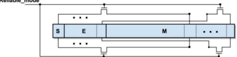
Based on these observations, we propose to comprehensively sacrifice the precision level for the sake of reliability. Practically, we suggest to utilise the least significant bits of the Mantissa within a floating point number to enhance the reliability of its critical bits, namely, Sign and Exponent bits. The bit-level reliability enhancement of the critical bits is performed by memory cells joining upon request to store a single bit of data into two cells as explained in Section 3. As shown in Fig. 8, the mode selection is
made through the ‘Reliable_mode’ signal. The joiners consist of NMOS transistors that can be triggered to activate reliability mode, or deactivated to switch to the precision mode. This circuit level property allows a comprehensive adaptation of the hardware to the application request as well as to the environmental conditions.
5 Experimental results
5.1 Setup
As explained in Section 3, we propose a reliability enhancement technique based on a circuit level adaptive 7T/14T technique altogether with architecture level organisation. Circuit characteristics of 7T/14T are explained in detail in the literature [12, 16]. For confirming circuit functionality and calculating area and power overheads, simulation with HSPICE was performed with 22 nm predictive technology model library [17]. Transistor sizes for typical 22 nm SRAM cell were chosen from [18]. Ratio values are: cell ratio = WPD/WPG = 2.02 and pullup ratio = WPU/WPG = 1.18. Wordline pulse width is chosen as 1 ns.
We selected typical values of original BER and SER and improved rates using 7T/14T SRAM cell form [16, 19]. Although those experimental results are related to SRAM chips fabricated in different technologies (65 and 150 nm), we only considered the normalised improvement, not the exact values.
• BER for read operation: 7T SRAM cell (same as 6T) = 5.0 × 10⁻⁴, 14T in dependable mode = 1.0 × 10⁻⁸ [16] (in [16] BER for write and hold are also available, but we took read as most critical one).
• SER of 14T is improved by 80% over SER of 7T SRAM cell (same as 6T) [19]. We assumed SER = 10−7 as typical unprotected SER [9].
Although SER per memory bit grows smoothly by technology size reduction [20], SER per system increases sharply. As mentioned before, 14 T structure has more noise margin and critical charge which is translated to more resistance against any instability including high energy particles or bit flipping during read operation [19].
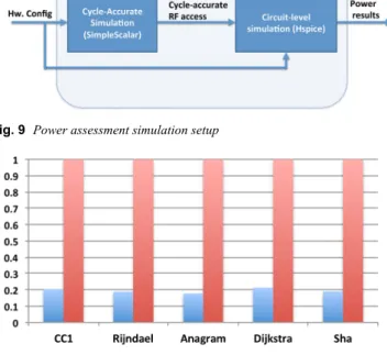
In this section, the system-level experiments are presented for a typical 32 × 32 bit RF, where power oriented experiments were conducted to verify the effectiveness of the proposed architecture. To get accurate simulation results, SimpleScalar simulation environment [21] was modified by estimating the cycle-accurate power consumption using HSPICE results. SimpleScalar is a cycle-level simulation platform of a 5-stage pipeline out-of-order Superscalar processor. We extensively modified the simulator code to support the proposed reliability enhancement technique. Fig. 9 shows the experimental setup to estimate power consumption.
For experimental evaluation, benchmarks from the MiBench benchmark suite [22] were compiled for the Alpha instruction set architecture.
5.2 Integer RF results
To evaluate the amount of error resilience of ARH RF, we developed an exhaustive fault injection platform where the injected error locality is randomly defined. Considering again the benchmark distribution depicted in Fig. 1, and aforementioned SER of protected and unprotected bits, normalised error rates are shown in Fig. 10.
The increase in static power because of joiner switches is small. When those switches are ON, it is expected that the same value of data is stored on both cells and they keep unchanged voltage on both sides. During a write operation, writing just effective length will save power and compensate the extra power for writing redundant data. Using the cycle-accurate behaviour simulator, the power oriented modifications track the accessed registers at run-time and compute the power values, cycle-by-cycle, based on the
hardware configuration and the HSPICE simulation results. The normalised power consumption results presented in Fig. 11 show that the overall power overhead does not exceed 12% in the worst case, while SECDED's power overhead is between 18 and 24%.
An operand detection circuit is very simple and it does not affect on clock time. Similarly, additional read multiplexers are simple and may have a small negative effect. For simplicity, they can be moved from the output of the RF stage to execution stage like in other studies [9] in case of an increase in clock time. For each pair of bits, two switches are added in between them. Depending on the type of switches and number of read and write ports present in the RF, the area overhead per register is found to be around 10% [16].
5.3 Floating point RF results
5.3.1 Power analysis: For estimating the power overhead of new
architecture, first we simulated different cell architectures individually, including standard 6T SRAM cell and 7T/14T cell. Static (idle) power and dynamic power of write operation are calculated for individual bits. For static power, we differentiate between the case when joiner switches are on (both half keep identical values) and when joiner switches are off (average of two situations when two bit values are same or not). Dynamic power of write operation is an average of two situations when bit value is changed or not changed. Corresponding results are shown in Table 1 (Vdd = 0.8 V, joiner type: minimum size NMOS).
New floating point register architecture has nine number of bits in the form of a 7T/14T. When a register is in reliable mode, joiners are active, otherwise register is similar to the conventional floating point. Using numbers in Table 1, power estimation for two types of 32-bit floating point register is estimated in Table 2. Results show that the proposed technique achieves significantly less power overhead when compared to SECDED. In fact, while SECDED results in 18% more static power than the baseline register, our technique results in 0.6% power overhead per bit.
5.3.2 Reliability-precision: We modified the SimpleScalar
simulator to support the new floating point RF architecture and utilised a probabilistic fault injection to measure the impact on reliability and results accuracy. We ran a set of benchmarks that manipulate floating point numbers and we used the mean normalised error distance (MNED) as a precision metric. The normalised error distance (ED) for a given operation is defined as follows:
NED = R − R*R , (2)
where R and R* are the results of the operation for golden run and modified RF, respectively. Hence, for a benchmark with a number of N calculated results, the MNED is given below:
MNED =∑ii= 0=N− 1NED
N (3)
To test the effectiveness of our approach, we performed several experiments while increasing the error rate within the RF architecture and record the MNED accordingly. We run three different benchmarks from Mibench using an augmented simulation environment built upon Simplescalar for three RF architectures:
• Baseline non protected RF. • The proposed RF.
• A RF architecture protected by Single Error Correct Double Error Detect (SECDED) mechanism.
All these experiments are conducted for SEU, Double Event Upset and Triple Event Upset case scenarios.
Fig. 12 shows the evolution of the average MNED in terms of the error rate for the three floating point benchmarks: FFT, Patricia
Fig. 9 Power assessment simulation setup
Fig. 10 Normalised error rate of ARH RF versus conventional RF
Fig. 11 Normalised power consumption of ARH RF versus conventional RF and SECDED protected RF
Table 1 Power results per bit
Cell type 6T Proposed
architecture (Reliable_mode = 1) Proposed architecture (Reliable_mode = 0) static power, pW 482 489 538 dynamic power per write, fJ 0.28 0.45 0.31
Table 2 Power numbers per register
Register type All bits
6T architecture (ReliableProposed _mode = 1)
SECDED
static power, nW 15.4 15.5 18.3 dynamic power per
write, fJ
and Basic Math. Those benchmarks are used to cover three different types of commonly used applications such as signal processing, telecommunication and mathematical problems solving. As the proposed RF protects bits with high impact on the result, the overall deviation keeps relatively small compared to the baseline RF. Here, we consider only SEUs and therefore SECDED is considered fully immune. Nevertheless, as shown in Fig. 13, SECDED consumes more power than the proposed RF. SECDED consumes around 19% of the overall processor power while the proposed approach power consumption is comparable to the baseline RF (14% of the overall processor power).
While SEU is a matter to be addressed nowadays in mainstream applications, MBUs constitute a major concern in aggressive environments. In fact, highly charged particles pass through the silicon as they can energise two or more adjacent memory cells simultaneously [23]. Fig. 14 represents the results of MNED in terms of error rate while considering double event upsets. It is worth noticing that, even if SECDED is able to detect a double bit flip, the correction leads to around 20% in terms of time penalty [24]. In fact, as shown in Fig. 15, the time redundancy after a double event detection result in a considerable time penalty that increases with the error rates.
As the number of flipped bits increases, the SECDED shows its limits because of the incapacity to detect three-bit flips. Fig. 16 shows that SECDED performs even worse results than the baseline RF under triple event upsets. Miss calculations in error correcting codes lead to flipping more bits instead of correcting the data.
5.4 Discussion
The proposed reliability enhancement techniques rely on both circuit-level and architecture-level aspects. This allows a considerable gain in power budget compared to the widely utilised ECCs. Moreover, the proposed floating point register file architecture is more efficient with high error rates, which makes it suitable for aggressive environment applications such as space and aerospace domains. While the proposed architecture offers a good tradeoff for approximate computing applications that may tolerate a range of output variability, it is not totally suitable for applications with high precision requirements.
The area overhead for our proposed scheme is estimated as follows. In our modified register file, 2-bit LE and one joiner transistor per 6T SRAM cell are added per 32-bit register, leading to 23% increase in transistor count. However, as pointed out in the introduction, generally in RF the performance is critical, not the area, where non-minimum size transistors are employed (unlike
Fig. 12 MNED for the proposed RF in terms of error rate compared to the baseline RF under Single Event Upset
Fig. 13 Power consumption of the tested RFs normalised to the total processor power consumption
Fig. 14 MNED for the proposed RF in terms of error rate compared to the baseline RF under Double Event Upset
Fig. 15 Execution time normalised to the baseline RF execution
Fig. 16 MNED for the proposed RF in terms of error rate compared to the baseline RF under Triple Event Upset
cache which is an area dominant unit). Moreover, standard 6T SRAM cell structure contains larger pull-down transistors. Since the joiner transistors can be selected from a minimum sized ones [13], the real overhead in layout area is considerably less, roughly down to 10%. As depicted in Fig. 5, modifications inside ALU and RF decoder, including adding a few primitive gates per 32-bit register and a single read access multiplexer for RF have negligible overheads, however the exact percentage depends on the actual architecture design which is not discussed here.
In terms of bit protection coverage, the maximum bit upsets that our proposed method can cover depends on the data length and the adjacent register effective length (EL). The maximum efficiency is attained when the first register has an EL = 3 Bytes, while the adjacent register's EL = 1 Byte. In this case, all bits could be protected, namely 32-bit upsets are supported. However, in the worst case where two adjacent registers have an EL = 4, none of them could be protected.
6 Conclusion and future work
This work proposes power efficient reliability enhancement for RFs in embedded systems. Specifically, in integer RFs, leading bits (0 or 1) are detected and used for cell radiation hardening in circuit level. This aspect not only provides protection to long-length values but also is very efficient in data hardening within critical applications. Moreover, we suggest a new reliability enhancement technique for floating point RFs. Specifically, we utilise the least significant bits of the Mantissa within an IEEE-754 floating point number to enhance the reliability of its critical bits (Exponent and Sign). We show that the average error distance is reduced significantly in comparison to baseline RF. The reliability gain of the proposed RF becomes even more significant with high error rates, which makes it suitable for aggressive environments like space applications.
Future work will extend the study to combinational circuits and functional units for a more comprehensive architecture.
7 References
[1] Reviriego, P., Maestro, J.A., Flanagan, M.F.: ‘Error detection in majority logic decoding of Euclidean geometry low density parity check (eg-ldpc) codes’, IEEE Trans. VLSI Syst., 2013, 21, pp. 156–159
[2] Guena, P.: ‘A cache primer’, Application Note Freescale Semiconductor, 2004
[3] Gherman, V., Evain, S., Seymour, N., et al.: ‘Generalized parity-check matrices for sec-ded codes with fixed parity’. 2011 IEEE 17th Int. On-Line Testing Symp. (IOLTS), Athens, Greece, 2011, pp. 198–201
[4] Ahangari, H., Alouani, I., Ozturk, O., et al.: ‘Register file reliability enhancement through adjacent narrow-width exploitation’. Int. Conf. on
Design and Technology of Integrated Systems in Nanoscale Era (DTIS 2016), Istanbul, Turkey, 2016, vol. 35
[5] ‘European Space Agency, ERC32’. Available at http:// microelectronics.esa.int/erc32/index.html
[6] Gaisler, J.: ‘A portable and fault-tolerant microprocessor based on the sparc v8 architecture’. Proc. Int. Conf. on Dependable Systems and Networks, Washington, DC, USA, 2002, pp. 409–415
[7] Villalpando, C., Rennels, D., Some, R., et al.: ‘Reliable multicore processors for nasa space missions’. 2011 Aerospace Conf., Big Sky, MT, USA, 2011, pp. 1–12
[8] Memik, G., Kandemir, M.T., Ozturk, O.: ‘Increasing register file immunity to transient errors’. Design, Automation and Test in Europe, Munich, Germany, 2005, vol. 1, pp. 586–591
[9] Hu, J., Wang, S., Ziavras, S.G.: ‘On the exploitation of narrow-width values for improving register file reliability’, IEEE Trans. Very Large Scale Integr. (VLSI) Syst., 2009, 17, (7), pp. 953–963
[10] Kandala, M., Zhang, W., Yang, L.T.: ‘An area-efficient approach to improving register file reliability against transient errors’. 21st Int. Conf. on Advanced Information Networking and ApplicationsWorkshops, 2007 (AINAW'07), Niagara Falls, Canada, 2007, vol. 1, pp. 798–803
[11] Shin, D., Gupta, S.K.: ‘Approximate logic synthesis for error tolerant applications’. 2010 Design, Automation Test in Europe Conf. Exhibition (DATE 2010), Dresden, Germany, 2010, pp. 957–960
[12] Fujiwara, H., Okumura, S., Iguchi, Y., et al.: ‘Quality of a bit (qob): A new concept in dependable sram’. 9th Int. Symp. on Quality Electronic Design (isqed 2008), San Jose, CA, USA, 2008, pp. 98–102
[13] Ahangari, H., Yalcin, G., Ozturk, O., et al.: ‘Jsram: A circuit-level technique for trading-off robustness and capacity in cache memories’. IEEE Computer Society Annual Symp. on VLSI, Montpellier, France, 2015, pp. 149–154 [14] Li, X., Yeung, D.: ‘Application-level correctness and its impact on fault
tolerance’. 2007 IEEE 13th Int. Symp. on High Performance Computer Architecture, Phoenix, AZ, USA, 2007, pp. 181–192
[15] Misailovic, S., Sidiroglou, S., Hoffmann, H., et al.: ‘Quality of service profiling’. Proc. of the 32Nd ACM/IEEE Int. Conf. on Software Engineering (ICSE ‘10), New York, NY, USA, 2010, vol. 1, pp. 25–34
[16] Fujiwara, H., Okumura, S., Iguchi, Y., et al.: ‘A 7t/14t dependable sram and its array structure to avoid half selection’. 2009 22nd Int. Conf. on VLSI Design, New Delhi, India, 2009, pp. 295–300
[17] ‘Predictive technology model (ptm) website’. Available at http:// www.cfreds.nist.gov/
[18] C., S., : ‘Advanced MOSFET designs and implications for SRAM scaling’. PhD Thesis, 2011
[19] Yoshimoto, S., Amashita, T., Okumura, S., et al.: ‘Bit error and soft error hardenable 7t/14t sram with 150-nm fd-soi process’. 2011 Int. Reliability Physics Symp., Monterey, CA, USA, 2011, pp. SE.3.1–SE.3.6
[20] Baumann, R.: ‘Soft errors in advanced computer systems’, Des. Test Comput., 2005, 22, (3), pp. 258–266
[21] Austin, T., Larson, E., Ernst, D.: ‘Simplescalar: an infrastructure for computer system modeling’, IEEE Comput., 2002, 35, pp. 59–67
[22] Guthaus, M.R., Ringenberg, J.S., Ernst, D., et al.: ‘Mibench: A free, commercially representative embedded benchmark suite’. 2001 IEEE Int. Workshop Proc. of the Workload Characterization 2001 (WWC-4), Austin, TX, USA, 2001
[23] Neale, A., Jonkman, M., Sachdev, M.: ‘Adjacent-mbu-tolerant sec-ded-taec-yaed codes for embedded srams’, IEEE Trans. Circuits Syst. II, Express Briefs, 2015, 62, (4), pp. 387–391
[24] Koren, I.: ‘Defect and fault tolerance in vlsi systems’, vol. 1, (Springer, New York, NY, USA, 2012)