339
Talha Erdem and Hilmi Volkan Demir
Bilkent University, Ankara, Turkey
12
ON - CHIP INTEGRATION OF
FUNCTIONAL HYBRID
MATERIALS AND
COMPONENTS IN
NANOPHOTONICS AND
OPTOELECTRONICS
Incorporation of custom - designed nanomaterial into nanophotonic devices and compo-nents in optoelectronic systems enables the realization of optical functionalities favor-ably controlled with external optical and electrical effects. To this end, innovative nanophotonic devices and optoelectronic systems are developed using multiple combi-nations of nanostructures (epitaxially grown, chemically synthesized, deposited, plated, etc.) that are embedded in hybrid architectures and on - chip integration of components for a variety of applications including light generation, displays, modulation, sensing, imaging, and communications in a wide spectral range from ultraviolet (UV) to visible to infrared.
Such integration of functional materials and components in optoelectronics requires the use of different methods developed for chip - scale integration at the range of microm-eters to nanommicrom-eters, including monolithic integration, hybrid integration, layer - by - layer assembly, and directed assemblies (electrical, optical, mechanical, etc.). This chapter reviews these state - of - the - art integration approaches currently used in optoelectronics.
Ceramic Integration and Joining Technologies: From Macro to Nanoscale, First Edition.
Edited by Mrityunjay Singh, Tatsuki Ohji, Rajiv Asthana, Sanjay Mathur.
340 ON-CHIP INTEGRATION IN NANOPHOTONICS AND OPTOELECTRONICS
Additionally, the chapter summarizes those innovative integration approaches that are presently being investigated for cutting - edge optoelectronics and nanophotonics.
MONOLITHIC INTEGRATION TECHNIQUES
Optoelectronic components used in current communication systems are typically based on discrete components. These components with different functions are generally com-bined with each other using fi ber splices to provide a specifi ed function. Although the approach of packaging each component individually and then connecting them through fi ber connections is a common practice, it manifests some disadvantages. One of them is the great diffi culty in effi ciently coupling light to and from each discrete chip, which is one of the main sources of optical loss at the system level. In addition, this approach also places a burden at the system implementation level due to cost issues.
To address these problems, monolithic integration may provide possible solutions
[1] . For example, using the on - chip integration method, device - to - device coupling
problem can be completely eliminated, conveniently leading to a signifi cant decrease in packaging costs and sizes. Additionally, elimination of possible mechanical move-ments in the structure and possible reduction of driving currents may reduce the power consumption of such integrated chips and may increase the reliability of the full system. For monolithic integration to become useful and meaningful, a list of some require-ments should be fulfi lled [2] :
1. The operation of one component should not be affected by the operation of the other components. In other words, each component should function as if it is discrete.
2. Trade - off between fabrication diffi culty and performance optimization should be carefully considered because a careless design may increase the overall cost and/or may decrease the device performance.
3. The integration method should not be costly and time - consuming. There are several monolithic integration schemes.
Butt Joint Growth
Butt joint growth is based on the removal of a specifi c part of the epitaxial region (e.g., waveguide/multiple quantum well [MQW] region and, subsequently, the nonplanar selective regrowth to fi ll in the removed part (e.g., with desired band edge and wave-guide architecture). The main advantage of this integration technique is its high versatil-ity [3] . An exemplary cross - section of butt joint grown epitaxy is shown in Figure 12.1 a. In this case, for example, for a laser diode, the fl exibility of this process comes from the possibility to grow a quantum well active region for a maximized modal gain. Also, allowing each growth to lead to a desired absorption band edge is an additional strength of this approach. In spite of the ability to separately optimize individual components on the chip [4] , there is also some diffi culty that arises with the requirement to match the growth thicknesses and to achieve the desired composition to avoid refl ection and
MONOLITHIC INTEGRATION TECHNIQUES 341
loss at the interfaces [3] . Increasing the number of desired band edges and waveguide architectures increases the complexity since each new band edge and structure requires an additional regrowth [4] .
Selective Area Growth ( SAG )
The SAG technique can be used effectively to provide multiple band edges across the epitaxial wafer in a single growth step [5] . This method involves patterning of a dielec-tric mask on the epiwafer, which is followed by the epitaxial growth (e.g., metal organic chemical vapor deposition [MOCVD] growth). This dielectric mask limits the growth. After butt joint growth, additional regrowth for the upper cladding is performed fol-lowing the removal of the dielectric mask (Fig. 12.1 b). For example, in the case of making a waveguide that integrates a laser diode with a modulator diode along the length of the waveguide, the centered multiple quantum well (c - MQW) active regions in the waveguide are grown on a single chip both for maximum gain in the laser diode section and for maximum electroabsorption in the quantum well electroabsorption modulator (QW EAM). As this technique is based on the contrast in the surface kinetics of the growth elements on the semiconductor and dielectric, the reactor conditions should be controlled very carefully. However, one problem is that the surface diffusion around the transition region might be on the order of tens of micrometers. Also, thick-ness variation may cause a nonideal optical mode overlap with the MQW region [4] .
Figure 12.1. (a) Butt joint growth, (b) selective area growth, and (c) offset quantum well techniques showing cross - sectional active and passive sections perpendicular to the growth direction [4] . (a) (b) (c) ACTIVE BUTT JOINT BEGROWTH SELECTIVE AREA GROWTH OFFSET QUANTUM WELLS PASSIVE ACTIVE PASSIVE ACTIVE PASSIVE
342 ON-CHIP INTEGRATION IN NANOPHOTONICS AND OPTOELECTRONICS
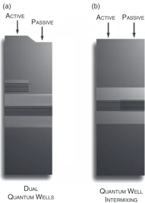
Offset Quantum Wells
This method involves the growth of the MQW active region on a passive bulk wave-guide. This technique allows the nonabsorbing waveguide section to be left for the selective etching of MQWs because the gain is not a concern in these etched regions. After building the active and passive regions, the upper cladding is regrown in this technique as well (Fig. 12.1 c) [6] . The strength of this technique lies in its simplicity. However, allowing only for two band edges at most (one from MQW and one from the waveguide) is a drawback of this method [4] .
The offset quantum well method can be improved with the addition of a wider band gap quantum well in the passive waveguide [6] , known as dual offset quantum wells, shown in Figure 12.2 a. This improvement provides more effi cient electroabsorp-tion and phase modulators by using a quantum - confi ned Stark effect resulting in a more abrupt absorption edge [2] .
Quantum Well Intermixing ( QWI )
Another method for the monolithic integration is the QWI technique. In this method, the metastable nature of gradient at the interfaces is used. Diffusion tendency under compositional/concentrational gradients is the driving force of this process. The diffu-sion rate can be adjusted/increased using catalysts. QWI process can be made selective by using a lithographically defi ned catalyst patterning. Some of the techniques used for
Figure 12.2. Schematics for (a) dual quantum wells and (b) quantum well intermixing methods [4] . (a) (b) ACTIVE QUANTUM WELL INTERMIXING DUAL QUANTUM WELLS
MONOLITHIC INTEGRATION TECHNIQUES 343
QWI are impurity - induced disordering (IID) [7] , impurity - free vacancy - enhanced disordering (IFVD) [8] , photoabsorption induced disdisordering (PAID) [9] , and implantation enhanced interdiffusion [10] . A schematic representation of the process is given in Figure 12.2 b. QWI does not change the average composition; however, it changes the compositional profi le slightly. Therefore, reasonable index continuity is observed at the interface between adjacent parts. This property of the QWI method avoids parasitic refl ections, which would otherwise decrease the performance of the device [4] .
Coldren and coworkers used the implant - enhanced interdiffusion technique to build up a 10 - Gb/s widely tunable transmitter. This technique involves the diffusion of point defects created during ion implantation into an InP implant buffer layer grown on an MQW active region [2] . Good spatial resolution and controllability (using annealing time, temperature, and implant dose) are the strengths of this method [11] .
The IID method relies on the use of impurities, generally dopants, to change the equilibrium defect concentration, which depends on the Fermi level to enhance self diffusion into the crystal resulting from intermixing [7] . A disadvantage of this method is the adverse effects of dopants on the electrical properties of the device [12] .
The PAID technique is based on the heating of the MQW structure through laser irradiation to provide intermixing [12] . The drawback of this technique is its poor spatial resolution, although the material quality is very high [9] .
The IFVD method relies on the postgrowth introduction of vacancies that diffuse through the lattice while exchanging places with adjacent atoms as a result of a thermal process. This diffusion mechanism is the driving force of the intermixing for this tech-nique. In spite of its advantage of simplicity, high annealing temperatures to adjust the quantum well are a disadvantage of this method [9] .
Multigrowth Monolithic Integration
Sabnis et al. proposed and demonstrated an improved version of multistep selective area growth (MSAG) monolithic integration technique [13] . This approach mainly consists of fi ve steps:
1. Proper MSAG surface preparation and device isolation are maintained by stop-ping the incorporation of buried epitaxial etch. Thanks to these layers, it is possible to integrate different epitaxial layers with clean and planar surfaces before epitaxial regrowths. Sequential surface preparation for MSAG can be realized by burying multiple etch - stop layers, one for every MSAG process. 2. Different epitaxial structures are combined by an MSAG process.
3. Device mesas in the SAG are constructed by an MSAG epitaxy etching while using selective wet etches and shallow dry etches.
4. Planarization and passivation processes are applied.
5. Another planarization and passivation process is applied to enable multilevel metal routing for maintaining the desired circuit architecture. After the wafer planarization, interconnection of metal from level to level is still needed. This requirement is fulfi lled by using vias and plug metallization. Another approach
344 ON-CHIP INTEGRATION IN NANOPHOTONICS AND OPTOELECTRONICS
is to etch the planarization material such that a slope is constructed at the inter-face between layers where the metal connection is desired.
These steps are shown in Figure 12.3 .
Surface Passivation and Planarization
During the selective removal of the epitaxially grown material by vertical etching, the sidewalls of the device are typically left exposed. These regions are chemically active and may introduce surface states, which further results in current leakage and stability problems. Sidewall passivation and planarization of the passivation material are therefore required procedures for the vertically etched III – V semiconductor devices [14] . The sidewall passivation suppresses the leakage current, whereas the planarization of the passivation material is needed for the metal interconnection and device integration.
In the etch - back planarization method [15] , which is a conventional approach, the planarization of the entire wafer is diffi cult to seal and passivate device sidewalls. To solve this problem, Demir et al. proposed an approach to realize self - aligning planariza-tion and passivaplanariza-tion. In this method, the passivaplanariza-tion is achieved by the use of a pas-sivation polymer to passivate the sidewalls across the epitaxial wafer.
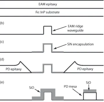
Figure 12.3. MSAG process for the monolithic integration of a photodetector (PD) and an electroabsorption modulator (EAM): (a) epitaxial growth of EAM, (b) ridge etching of EAM, (c) SiN mask defi nition for SAG, (d) PD SAG, and (e) PD mesa etch [13] .
(a)
(b)
(c)
(d)
MONOLITHIC INTEGRATION TECHNIQUES 345
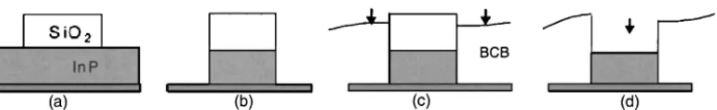
The process can be summarized in Figure 12.4 as follows: (1) A dielectric mask is defi ned on the wafer, which is maintained in the subsequent steps; (2) by vertically etching the unmasked parts of the wafer, the semiconductor device area, which is masked, is defi ned; (3) the sidewalls of the semiconductor mesa are selectively etched horizontally to form an undercut beneath the hard mask to protect the device as a roof; (4) the sidewalls of the device layers under the hard mask are sealed and passivated with a spin - on polymer; (5) the cured polymer past the top level of the hard mask is etched back with an anisotropic dry etch; and (6) the hard mask is removed in order to construct a passivation structure with the polymer around the device perimeter. In this work, benzocyclobutene (BCB) is used as the passivation polymer, while silicon nitride or silicon oxide is used as the hard mask [16] .
Via and Trench Building for Metal Contacts
In III – V semiconductor materials, vias and trenches are used for metal contacting [17] . In the work of Zheng et al., the construction of these structures involves the use of a
sacrifi cial layer, which is made of either a SiO 2 dielectric hard mask layer on the device
layers or a semiconductor layer grown onto the device epitaxial layer, both before pat-terning. The construction steps follow: (1) formation of a hard mask using conventional dielectric thin - fi lm deposition, (2) etching of the semiconductor by reactive ion etching using the hard mask, (3) spinning of a polymer layer and back etching within the hard mask for every device in the wafer, and (4) removal of the hard mask by wet etching to have a via structure. This procedure is illustrated in Figure 12.5 .
Figure 12.4. Illustration of self - planarizing passivation sequence: (a) The hard mask on the epitaxial wafer is defi ned; (b) device areas are patterned by vertical etching; (c) the device materials underlying the hard mask perimeters are removed for the undercut creation; (d) the device areas are sealed; (e) the cured polymer is etched back; and (f) the hard mask is removed [14] .
346 ON-CHIP INTEGRATION IN NANOPHOTONICS AND OPTOELECTRONICS
NANOFABRICATION TECHNIQUES
Nanoscale material design and nanoscale fabrication techniques are in general grouped as top - down and bottom - up approaches [18] . The top - down method involves various techniques of lithography to pattern nanoscale structures. This approach may make use of serial and parallel techniques to pattern features. On the other hand, the bottom - up method is based on the interactions between molecules and colloidal particles to con-struct discrete nanoscale con-structures in two and three dimensions.
Photolithography and scanning beam lithography are considered in the conven-tional top - down approach. Their limitations are their high costs, diffi culty in accessing the required facilities, and lack of applicability in a wide range of problems. Less
con-ventional approaches also cover both top - down and bottom - up methods. Molding,
embossing, and printing can be classifi ed as top - down methods; on the other hand, scanning probe lithography (SPL), edge lithography, and self - assembly can be inter-preted as bridge methods between the top - down and bottom - up approaches.
In general, conventional techniques suffer high cost and low throughput, and they are typically restricted to planar fabrication in semiconductor materials and are incom-patible with many problems in nonstandard fabrication. Additionally, these techniques expose substrates to corrosive etchants, cause high - energy radiation, and require high temperatures. These are the driving force for the investigation of new nanofabrication methods.
Photolithography
Photolithography is the chosen method for the manufacturing of microelectronic devices by the industry. In photolithographic systems, mask aligners shine collimated light trough a quartz plate that supports a patterned chromium coating and expose a photoresist thin fi lm coated on a planar substrate. The photoresist is an organic material that becomes insoluble or more soluble as a result of chemical changes when exposed to high - energy (short wavelength) light [19 – 21] . The photoresist exposed to light is soaked in a solvent that dissolves exposed or unexposed regions. This process thus allows for transferring the pattern of the starting mask to the exposed and developed photoresist fi lm on the substrate. This patterning also functions as a mask for the substrate during subsequent steps (Fig. 12.6 ). A modern photolithography system can pattern with a resolution of 27 nm [22] . In 2005 semiconductor nanofabrication productions, photolithography is used
Figure 12.5. Schematic illustration of via and trench formation: (a) formation of the hard mask, (b) etching the semiconductor to defi ne the active region, (c) spinning and back etching of the polymer, and (d) removal of the hard mask to obtain via and trench opening [17] .
NANOFABRICATION TECHNIQUES 347
to pattern 37 - nm - wide features with 193 - nm wavelength light. Attempts to decrease these sizes require optical proximity correction (OPC) and phase - shift mask technology; however, all of these modifi cations increase the cost signifi cantly.
Immersion lithography is proposed as a potential lithography method for features with sub - 50 - nm resolution exposing light at 193 nm [23] . This lithography technique is the analogous of immersion microscopy that is widely used in biology [24] . In this technology, the imaging resolution is improved by the increased refractive index of the medium between the imaging lens and the imaging plane [24] . This method requires contacting the photoresist - coated substrate and mask with water (or another solvent) and using complex, aspheric, catadioptric lenses. Another solution toward patterning smaller structures using photolithography might be decreasing the wavelength of expos-ing light. This, however, requires new types of photoresists, new light sources, and new types of optics.
Figure 12.6. Schematic illustration of fabrication using photolithography and electroplating in hard materials [18] . Develop photoresist Remove photoresist Separate Photoresist Si/Quartz Si/Quartz Si/Quartz Si/Quartz Si/Quartz Si/Quartz Metal Metal Write with scanning beam (or)
Dry etch Depositmetal film
Electroplate metal Mask and
348 ON-CHIP INTEGRATION IN NANOPHOTONICS AND OPTOELECTRONICS
The main drawback of the photolithography lies on the time and cost requirements to fabricate the photomask. On the other hand, interferometric lithography provides the production of simple patterns without using a photomask [25, 26] . This method is based on the constructive and destructive interference of multiple laser beams at the surface of photoresist. Although no photomask is needed for this method, pattern projection is restricted only for regularly spaced arrays.
Scanning Beam Lithography
Scanning beam lithography is a process that is often used for the production of photo-masks for projection lithography instead of actual device fabrication. Patterning dense
arrays of sub - 20 - nm features on an area of 1 cm 2
takes ca. 24 h [18] . Therefore, scanning beam lithography is restricted to small areas or to areas with low densities.
Scanning beam lithography is a slow process compared to photolithography. However, this technique also allows for the fabrication of arbitrary patterns. Scanning beam lithography has three classes: (1) scanned laser beams with ca. 250 - nm resolution
(the least expensive), (2) focused electron beams with sub - 50 - nm resolution, and
(3) focused ion beam (FIB) lithography systems with sub - 50 - nm resolution (often used in research).
High - resolution patterning comes with some trade - offs. An increase in the resolu-tion can be achieved only by decreasing the diameter of the particle beam. As a result, the beam current also decreases, which results in an increased processing time, required to pattern the entire surface.
An FIB enables writing patterns into a photoresist or directly onto the substrate [27] . Using this technique, materials can be selectively removed through ion bombard-ment, or patterns can be created additively by localized chemical vapor deposition or by ion deposition [28 – 30] . FIB lithography enables patterning features in a semiconduc-tor with resolution down to 20 nm and with lateral dimensions down to 5 nm [31] .
SPL
SPL is a promising tool for manipulation and imagination with an atomic - scale resolu-tion [32] . However, this tool requires improvements for use in large - area manufactur-ing. Scanning tunneling microscopy (STM) (Fig. 12.7 A), atomic force microscopy (AFM), and near - fi eld scanning optical microscopy (NSOM) are some of the most important SPL techniques. Although atomic - scale manipulations on surfaces are pos-sible using these techniques, there is still a long way to go in order to make these techniques practical [18] . In general, the operation of SPL can be described as the localized modifi cation of surface by oxidation or by material transfer using a sharp probe in contact with the surface [18, 33, 34] .
Serial Patterning of Surfaces
Dip - pen nanolithography (DPN) provides methods to dispose nanoparticles or other molecules selectively onto a surface [34] . Inking AFM tips with a solution of the materials to be transferred enables positioning the material onto the substrate when the
Figure 12.7.
Schematic illustrations of four approaches to SPL and patterns produced using (A) STM
[35]
(B) to make a quantum corral
of a 48
- atom Fe ring formed on Cu enclosing a defect
- free region [198] ; (C) dip - pen lithography (DPN) [35] (D) to pattern features down to 15 nm [199] ; (E) nanoshaving [35]
to remove regions of SAMs (F) to pattern a square hole within octadecane thiolate SAMs
on Au
[200]
, and (G) scanning electrochemical oxidation
[35]
to selectively oxidize a surface (H) to build ca. 50
- nm
- wide lines of oxide
written on T iN [38] . (b) (f) (d) (h) (e) (a) S TM T ip AFM T ip AFM T ip AFM T ip Mat er ial T ransf er Scan Dir ection V V Scan Dir ection Scan Dir ection Scan Dir ection Applies Load Cu (1 11) Substr a te A u Substr at e A u Substr at e Wa te r Wa te r Oxide T iN F ilm Fe Fe Fe (g) 1 nm 50 nm 50 nm 1 5 nm 0.1 5 µ m 250 nm (c) 349
350 ON-CHIP INTEGRATION IN NANOPHOTONICS AND OPTOELECTRONICS
probe scans the surface (Fig. 12.7 C) [35] . Using DPN 15 - nm patterns is achievable (Fig. 12.7 D). This mechanism cannot be understood perfectly; however, several theo-ries have been proposed. According to one theory, a water layer between the tip and surface makes the material transfer possible. According to another one, the material transfer is possible due to the solid – solid interactions. Humidity, chemical interaction with the substrate, radius of curvature of the probe, and linear velocity of the probe determine the spreading of the ink.
Another approach for the patterning of the surfaces is the selective removal of material from the surface. This removal operation is performed by mechanical abrasion using a scanned AFM probe [36] . The probe displaces a thin fi lm when the contact load between the tip and the substrate is higher than the displacement threshold of the surface layer. This process is called “ nanoshaving, ” and it is used for the patterned removal of the self - assembled monolayers (SAMs) (Fig. 12.7 E, F) [20] . Material abrasion can also be performed after multiple scans when the contact load of the AFM tip is still below the displacement threshold of the material [37] . Nonuniformities in the topography, however, can cause irregular patterns. A surface can be chemically modifi ed using SPL. This operation can be made using a conductive AFM or STM tip. In Figure 12.7 G, H, a TiN substrate patterned by localized electric fi eld - induced oxidation using a conduc-tive AFM probe is shown [38] .
Parallel Patterning of Surfaces
Although SPL methods provide fl exible patterning possibilities, the use of a single tip makes these methods impractical for mass production. Using multiple probes that work in parallel may remedy this problem [35, 39] . A two - dimensional array of independently addressed AFM probe is developed, and this concept is known as “ millipede ” (Fig. 12.8 ) [39] . In this approach, defl ection in the vertical direction and resistive heating can also be provided.
NANOFABRICATION TECHNIQUES 351
Edge Lithography
In edge lithography, topographic edges are used in the fabrication of nanoscale struc-tures [35, 40, 41] . By using this method, arrays of strucstruc-tures that are smaller than 100 nm can be produced. Edge lithography can be grouped in two techniques: (1) edge lithography using topography - directed pattern transfer and (2) cleaved or cut edge nanostructures.
Pattern Transfer Directed by Topography. Decoration of step edges: At the step edges of single - crystalline surfaces, metals and other materials are deposited selectively with success [42, 43] . This deposition procedure results in the generation of continuous nanowires.
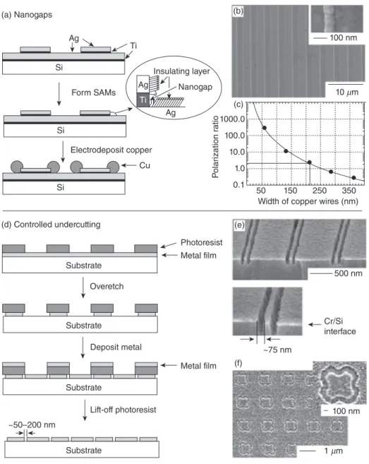
Electrodeposition or etching at the edge defi ned defects in SAMs: Selective removal and deposition of materials are the other ways of patterning nanostructures. [40, 44, 45] An example might be that sharp metal corners within topographically patterned metal substrates avoiding well - ordered SAM formation expose underlying metal at the edges (Fig. 12.9 A) [45] . Selective etching of this metal makes it possible to transfer the outline of the patterned metallic topography onto the underlying fi lm.
For example, SAMs can be formed on silver, but not on titanium, when the
pat-terned substrate is put into an alkanethiol solution. The exposed Ti/TiO 2 layer builds a
∼ 5 - nm gap in the SAM. This gap may serve as a nanoelectrode upon which metal can be electrochemically deposited (Fig. 12.9 B) [31] . A curved or fl at substrate can be produced while using an adhesive to remove these structures. Incident light can be polarized using the arrays of Cu lines on an adhesive (Fig. 12.9 C) [45] .
Controlling undercutting at edges: After the deposition of a thin fi lm, topographic features can be undercut in a controlled fashion. This technique also provides the fab-rication of nanostructures (Fig. 12.9 D) [44] . For example, isotropic wet etching of a
thin metal fi lm on a silicon or CaF 2 substrate covered with a photoresist provides
pat-terned structures following the undercutting of the photoresist [44] . Trenches at the edges of the pattern can be observed by lifting off the photoresist (Fig. 12.9 E, F) [44] . Phase - shifting photolithography: Controlling the phase of the exposing light, which is used to create narrow constructive and destructive interference, allows for signifi cant modifi cations in the intensity profi le when the light meets the vertical edges of a trans-parent, topographically patterned substrate. This phenomenon is used to create dark and bright spots of incident light onto the photoresist. Optimally, the light should have a
phase shift of π at the photoresist – mask interface.
Cleaved or Cut Edge Nanostructures. Various techniques to grow thin fi lms with a careful control of thickness between 1 and 50 nm enable additional following methods for the fabrication of nanostructures.
Edges Produced by Fracture . Simple quantum structures can be patterned using
the cross - sections of multilayer fi lms produced by molecular beam epitaxy
(MBE) as templates [41] . For example, fi eld - effect transistors (FETs) with a 20 - nm gate length are produced using this procedure. In this example, alternating
352 ON-CHIP INTEGRATION IN NANOPHOTONICS AND OPTOELECTRONICS
Figure 12.9. (A) Production of nanogaps by engineering defects in Ag SAMs, (B) scanning electron microscope (SEM) image of 70 - nm - wide lines of Cu selectively electrodeposited on these nanogaps [45] , (C) polarization ratio of the electric component of light as a function of line width [45] , (D) illustration of controlling undercutting, (E) cross - section of ∼ 75 - nm - wide trenches in silicon [44] , and (F) frequency - selective surface of 100 - nm - wide trenches in Al [44] . (a) Nanogaps Ag Ti Si Si Si Form SAMs Electrodeposit copper Cu Ag Substrate Substrate Substrate Substrate ~50–200 nm ~75 nm Cr/Si interface 500 nm 1 µm 10 µm 100 nm 100 nm
Width of copper wires (nm) 50 0.1 1.0 10.0 100.0 1000.0 150 250 350 P olar ization r a tio Photoresist Metal film Metal film Overetch Deposit metal Lift-off photoresist Ag Insulating layer Nanogap Ti (d) Controlled undercutting (b) (c) (e) (f)
NANOFABRICATION TECHNIQUES 353
layers of AlGaAs and GaAs, which are grown using MBE, are used (Fig. 12.10 A, B) [41] . Parallel arrays of nanowires can be built using selectively etched, mul-tilayered MBE - grown GaAs/AlGaAs substrates as the physical templates with narrowly spaced groves for patterning by physical vapor deposition (PVD). The widths of the wires are determined by the GaAs layers, and the spacing between wires is controlled by AlGaAs layers [46] .
Edges Produced by Sectioning with a Microtome . A nanostructured edge can be built up by embedding a thin fi lm in a matrix and by taking its cross - section. One approach to do this is based on removing the matrix material by repeated sliding against a rough surface [47, 48] . This technique can be extended using
a microtome to section a polymer - encapsulated patterned metal fi lm (Fig.
12.10 C, D) [49, 50] .
Edges Positioned by Reorientation . Tipping periodic arrays of posts onto one side
can be used to pattern large - scaled areas ( ∼ cm 2
) (Fig. 12.10 E) [51] . This process enables one to generate regular arrays of features in nanoscale lateral dimen-sions in plane (Fig. 12.10 F, G).
Soft Lithography
Soft lithography is a collection of techniques that involve organic (soft) materials to provide replication and pattern transfer on a wide range of length scales (from nano-meter to centinano-meter) [41] . The term soft is used for the stamp and/or substrate composed of materials including polymers or SAMs. The pattern transfer is achieved generally by fi rst fabricating a topographical patterned master then molding this master to build up a patterned stamp, and fi nally generating a replica of the original template (Fig. 12.11 ). Conventional methods are good enough for the fabrication of masters, whereas the rest of the process needs new techniques. Soft lithography can be described in three steps: replica molding, embossing, and microcontact printing.
Replica Molding. Replica molding transfers topographical features from a rigid or elastomeric mold into another material by solidifying a liquid in contact with the original pattern [52] . Step - and - fl ash lithography technique (Fig. 12.12 A), developed by Willson and colleagues, involves the use of a transparent master, for example, quartz [53] . After contacting this mold with a low - viscosity, photocurable polymer, the polymer is held under UV light. With this method, features as small as 30 nm can be produced
[54] . The strengths of this approach are the rapid cyclic time ( < 5 min/replication) and
the ability of optical mold alignment with features on the underlying surface [53, 55] . However, the diffi culty of patterning nanostructures on nonplanar surfaces replicating isolated features caused by air at the mold – polymer interface is the weakness of this technique. Replica molding can also be achieved using deformable templates, for example, polydimethlysiloxane (PDMS). Figure 12.12 B makes an illustrative summary of this procedure. Another way for the replica molding is the microtransfer molding, in which the liquid prepolymer is put into the molding regions. After cleaning the excess polymer using a fl at edge (a doctor blade), the mold is placed in contact with the rigid substrate. Finally, the prepolymer is cured (Fig. 12.12 C). This technique is used for
Figure 12.10.
(A) A schematic illustration and (B) SEM images of Pt nanowire arrays
[41]
, (C) illustration of the fabrication of a
pat-terned array of epoxy
- embedded conducting metal edges, (D) SEM image of these metal edges
[41]
, (E) schematic illustration of
micro-domino array uniformly collapsed after the application of a horizontal shear (PDMS)
[42]
, (F) SEM images of these structures, and
(G) a
∼
15
- nm
- wide edge of Pd on a collapsed post
[42]
. BOE, buf
fered oxide etch.
(a) GaAs Place on adhesiv e Al0.8 Ga 0.2 As R emo v e templat e PDMS mold Epo xy Epo xy Epo xy Section Hor iz ont al shear PDMS PDMS PDMS PDMS PDMS Deposit met al Si Pd θ − 20 ° Silicon w a fe r Separ at e R o ta te PDMS Pd edge Pd edge SU-8 SU-8 SU-8 R emo v e mold, deposit met al 50-nm A u f ilm Embed in epo xy , cur e BOE Deposit Pt Plasma clean 50 nm (b) (d) (f) (g) 1 4.5-nm Pd (c) (e) 1 µ m 15 µ m 5 µ m 354
Figure 12.11. Schematic illustration of soft lithography [35] . (Master)
(Replica)
Mold prepolymer
Cure, remove mold Photoresist
Si
Si
Cure, peel off PDMS (Stamp/Mold)
L D
H
Coat with PDMS prepolymer
PDMS
PDMS
PDMS
Figure 12.12. Schematic illustrations of molding techniques: (A) step and fl ash, (B) replica molding (RM), (C) microtransfer molding ( µ TM), and (D) micromolding in capillaries (MIMIC) [35] .
Release layer Liquid prepolymer Press template into prepolymer
UV cure, remove template
Cure, remove mold
Cure, remove mold Place on solid support Remove excess prepolymer
Cure prepolymer, remove mold Mold prepolymer Substrate Substrate Substrate Substrate Substrate Substrate Substrate Substrate Liquid prepolymer Liquid prepolymer Fill channels by capillarity Open channel Quartz PDMS PDMS PDMS PDMS PDMS PDMS PDMS Quartz (a) Step-and-flash (b) RM (d) MIMIC (c) µTM 355
356 ON-CHIP INTEGRATION IN NANOPHOTONICS AND OPTOELECTRONICS
patterning planar or curved surfaces [56] . Micromolding in capillaries is also another way of molding [57] . This technique involves the use of capillaries to fi ll the channels of a topographically patterned stamp with a liquid. The precursor material is cured within the capillaries and the mold is removed (Fig. 12.12 D).
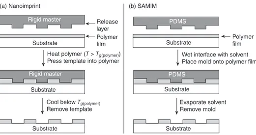
Embossing and Nanoimprinting. Embossing techniques are used for manufactur-ing compact disks and digital versatile disks (DVDs). The modifi cations of these techniques can also be extended to nanofabrication with a resolution below 50 nm [58] . Nanoimprint lithography is used to transfer a pattern from a rigid mold into a deform-able material coated on a rigid surface (Fig. 12.13 A). In general, the material is fi rst heated under pressure. The mold is later removed after cooling the material below its glass transition temperature. A structure that is as small as 10 nm can be replicated using imprinting with aspect ratios 10:1 [59] . In this technique, rigid mold and spin - cast polymer fi lm must be positioned in parallel, and the applied pressure should be uniform. These are the main drawbacks of this approach.
Embossing can also be applied using soft mold. Using PDMS mold solvent
assisted micromolding (SAMIM) takes place with an appropriate solvent instead of
using rigid mold, high temperatures, or pressures (Fig. 12.13 B). After placing the
polymer into the mold, evaporation is completed and, fi nally, the mold is removed.
Microcontact Printing. The general procedure for microcontact printing involves contacting the surface of a metal, metaloxide, or semiconductor with a topographically patterned PDMS stamp, wetted with a solution of an alkanethiol or other molecules that can form SAMs for a few seconds. An ordered monolayer is rapidly formed at the points of contact. The strengths of microcontact imprinting for fabricating nanoscale structures are that the minimum feature size on the pattern depends on the physical
Figure 12.13. Illustration of embossing procedures: (A) nanoimprint lithography and (B) solvent - assisted micromolding (SAMIM) [35] .
Release layer
(a) Nanoimprint (b) SAMIM
Polymer film
Polymer film Wet interface with solvent Place mold onto polymer film
Evaporate solvent Remove mold Substrate Substrate Substrate Substrate
Cool below Tg(polymer)
Remove template
Heat polymer (T > Tg(polymer))
Press template into polymer
Substrate Substrate PDMS PDMS Rigid master Rigid master
GENERAL SELF-ASSEMBLY TECHNIQUES 357
dimensions of the step (instead of optical diffraction), that the stamp provides mechani-cal fl exibility, and that various types of materials can be used as inks on different materials. Blurring of pattern by lateral diffusion of the ink, the deformation in the pattern refl ecting deformations in the stamp, and high number of defects in the fi lm are, on the other hand, the disadvantages of this technique [60] .
GENERAL SELF - ASSEMBLY TECHNIQUES
Self - assembly is defi ned as the self - organization of different components into regular structures without human intervention. Self - assembly processes can be observed and used in various fi elds of technology and nature. For nanotechnology, self - assembly appears to be one of the fundamental and most promising techniques to construct nanostructures. Self assembly can be classifi ed mainly into two groups: static self assembly and dynamic self - assembly.
Static self - assembly is based on the systems that are in equilibrium and that do not dissipate energy (Fig. 12.14 ) [61] . Molecular crystals and globular proteins are among the examples [62, 63] . Structures formed by static self - assembly may require energy during their building process; however, once they are formed, the structure is stable and therefore no energy is further needed to hold the system stable. Most of the research projects focus on this type of self - assembly.
In self - assembly, the components should be able to change their positions with respect to each other so that they can balance attractive and repulsive forces in their steady - state position. In molecular scale, these forces are often observed as the results of van der Waals, electrostatic, hydrophobic, and hydrophilic interactions. The forces observed in the self - assembly of larger structures include gravitational force, external electromagnetic forces, and magnetic, capillary, and entropic forces. Since the move-ment of particles is critical for the self - assembly processes, the interactions occur often in liquid media or on smooth surfaces.
Although researches are mainly focused on static self assembly, dynamic self assembly also has a signifi cant importance (Fig. 12.15 ) [60] . The main essence of dynamic self - assembly is to mimic the reactions and structures that enable the continu-ity of life in nature. In living cells, many self - assembly processes are dynamic. When the energy fl ow stops, these cells die, showing the importance of these processes.
Dynamic self - assembly can also be observed in nonliving environments and
systems. Oscillating reactions in solution and on the surface of catalysts, Rayleigh – Bernard convection cells are some examples for dynamic self - assembly.
Templated Self - Assembly
Templating self - assembly makes the creation of patterns into a self - assembled structure possible [20] . Additionally, it is used for increasing the order of the self - assembled structure. Surface topography, electric and magnetic fi elds, or shear forces can be used to direct self - assembly. Top - down methods to direct the bottom - up assembly of mole-cules and other particles are often preferred in the templated self - assembly approach [64] .
Figure 12.14. Examples of static self - assembly: (A) crystal structure of a ribosome [201] , (B) self - assembled peptide - amphiphile nanofi bers [95] , (C) an array of millimeter - sized poly-meric plates [61] , (D) thin fi lm of a nematic liquid crystal on an isotropic substrate [61] , (E) micrometer sized metallic polyhedra folded from planar substrates [202] , and (F) a three dimensional aggregate of micrometer plates [203] . (D) Courtesy of O. Lavrentovich.
(a) (e) (b) (c) (d) (f) 358
Figure 12.15. Examples of dynamic self - assembly: (A) an optical micrograph of a cell [204] , (B) reaction – diffusion waves in Belousov – Zabatinski reaction [61] , (C) a simple aggregate of a magnetized disk [205] , (D) a school of fi sh [61] , (E) concentric rings by charged metallic beads [61] , and (F) convection cells above a metallic support [61] .
(a) (d)
(b) (e)
(c) (f)
360 ON-CHIP INTEGRATION IN NANOPHOTONICS AND OPTOELECTRONICS
Templating from Molecules. Some organic nanostructures, which are not totally functional, can be used as templates to mask the deposition of metal or to guide the deposition of metal nanoparticles and nanowires [65, 66] . Patterning block copolymers
can be achieved by the combined usage of top - down and bottom - up approaches.
Extreme ultraviolet (EUV) interferometric lithography can be used to pattern oxidized SAMs or random copolymers on silica [67] . When a block of copolymer is made to self - assemble, the patterned SAM has the role of a template that guides the phase sepa-ration of the polymer. Moreover, regular copolymer structures can also be formed by annealing a block copolymer fi lm confi ned by physical boundaries [68] . Low level of defects, ability to control and pattern the phase - segregated regions, and controlled drift in the pattern over nonlocal dimensions are the advantages of this approach compared to nontemplated self - assembly.
Templating from Polymers. The modifi cation of colloidal particle surfaces can be realized by using charged polymers and polyelectrodes [69] . Electrostatic attraction between charged surface and charged particles suffi ces for the adsorption. In most of the cases, polymers have excess charge; therefore, they change/reverse the charge on the surface [70] . This electrostatic change on the surface allows for the formation of another polymer layer, which has the oppositely signed charge of the fi rst polymer layer. As a result, a layer - by - layer assembly process is observed. Colloidal particles are also
used to template the self - assembly of nanoparticles that have diameters of > 100 nm in
general [71] .
Templating Using External Forces. Nanospheres with similar sizes and shapes can be employed in the production of thin fi lms of ordered lattices by using their ten-dency to self - assemble. In order to direct the self - assembly of nanoparticles and nano-rods with different structures, electric [72] , magnetic [73] , shear forces [74] , and additional spatial constraints [75] are used. Compared to nanospheres, the self - assembly of nanowires and nanorods is more diffi cult because these nanostructures have aniso-tropic forms [76] . Self - assembled nanowires are observed in partially ordered, small domains.
According to another classifi cation of templated self - assembly, there are three main approaches; these are patterned chemical modifi cations of the surface, patterned charge, and patterned topography [77] . Preferential adsorption of particles on to the selected regions can be observed using the fi rst approach, that is, patterned chemical modifi ca-tions of the surface of the substrate [78] . The second approach can be realized by using FIB radiation [79] , microcontact printing of alkanethiols on gold [80] , selective adsorp-tion of polyelectrolytes [81] , and electrostatic microcontact printing [82] . Well - ordered high - quality lattices could not be observed using these methods. In order to confi ne and control colloidal assemblies, patterned topography of the substrate, like wells [83] , lithographically patterned reliefs [84] , or microfl uidic channels [85] are used in the literature. The ratio of the size of the particle to the size of the patterned feature affects the formation of the resulting lattices [86] . Also, shape - selective reliefs, physical bound-aries, and external fi elds are effective on the form of the lattice. An example of such a process is illustrated in Figure 12.16 [77] .
GENERAL SELF-ASSEMBLY TECHNIQUES 361
Figure 12.16. Schematic representation of template - directed self - assembly microspheres on a patterned gold electrode using an applied electric fi eld: (a, b) microcontact printing and etching building a templated electrode; (c, d) microspheres self - assembled over the templated electrodes under − 20 - kV voltage applied to gold electrode; (e) ideally, one microsphere remained on each window and no microspheres on the gold surface; and (f) a typical large area square matrix of microspheres [77] .
(a) PDMS stamp Cr/Au film Cr/Au film Polystyrene Polystyrene (1) Remove PDMS stamp (2) Cr/Ag etch Spherical beads Apply −20-kV mechanical agitation Pour excess spheres on electrode (b) (c) (d) (e) 1 mm (f)
362 ON-CHIP INTEGRATION IN NANOPHOTONICS AND OPTOELECTRONICS
Inorganic Templates. Alumina nanoholes and inorganic nanowires are success-fully used in the templated self - assembly of nanoparticles [87] . These provide better toughness and prevent changes in the structural characteristics of nanoparticles [88] . Wirelike or rodlike nanostructures are assembled by using alumina nanoholes as tem-plates, which are created by electrochemical etching. Anodic porous aluminas serve as nanocells that are used by building various nanostructured arrays, like magnetic nanorod arrays for longitudinal magnetic data storage, semiconductor particles for optical devices [89] , and electroluminescence display devices [90] . These arrays can be used in assembling large - area arrays of parallel wires.
Nanoparticle assembly can be realized both inside and outside these nanowires/ rods. As an example, the work of Ajayan and Iijima can be shown, in which they arrange Pd nanoparticles into the carbon nanotubes using capillary forces [91] . Nanoparticles can be assembled outside of these nanotemplates by direct deposition of material (physical or chemical deposition), sol – gel approach, or modifi cations of the surface functionalities [92] .
Biological Templates. Motivation for the use of self - assembly in nanofabrication comes from the observation that many biological structures are assembled by the molecular - level self - assembly [93] . DNA strands [94] , peptides [95] , and viruses [96] are the possible templates on which a signifi cant amount of research work currently continues. Covalent and noncovalent interactions are in charge during the assembly of nanostructures on these templates. Direct deposition or in situ growth of nanoparticles on these templates can be realized.
Chemically Assisted Assembly
Highly ordered nanoparticle assemblies or patterns can be created using a chemically assisted self - assembly technique [87, 97] . This technique is based on the covalent and noncovalent interactions of a nanoparticle surface protecting group. This approach is widely preferred both in solution and on surfaces. Chemically assisted self - assembly of nanoparticles can be applied by electrostatic layer - by - layer assembly, chemical templating, and SAM methods.
Hydrogen Bonding. Hydrogen bonding is one of the most investigated interaction types for the assembly of nanoparticles together with electrostatic interactions. Based on the hydrogen bonding phenomena, the exchange cross - linking precipitation route for nanoparticle assembly on surfaces is developed. Zirbs et al. showed, for example, the highly selective assembly of barbituric acid - stabilized Au nanoparticles onto Au substrates covered with Hamiltonian - type receptors (Fig. 12.17 ) [98] .
Additionally, different biomolecular linkers are also used for the assembly of nanoparticles based on hydrogen bonding [99] . The chemical characteristics of these molecules are very critical in order to realize the assembly of nanoparticles such as antibody – antigen interactions [100] .
GENERAL SELF-ASSEMBLY TECHNIQUES 363
Electrostatic Assembly. Simple and fl exible layer - by - layer assembled
nanostruc-tures can be created using electrostatic interactions (Fig. 12.18 ) [87] . Using this
approach, different materials with various optical and electronic properties are struc-tured. The layer - by - layer assembly is fi rst declared by Decher using polyelectroytes [69] , whereas Iler reported it for macroscale colloids [101] . However, the use of this technique for nanoparticle assembly is reported by Kotov et al. for the fi rst time [102] .
Entropic, van der Waals, steric, dipolar forces and electric charges on the sterically charged nanoparticles are effective in the determination of the stoichiometry of the structures. In general, the nanoparticles are negatively charged, whereas the polymer has a positive charge.
Layer - by - layer assembly is also possible by the epitaxial growth of layers. This technique is especially preferred in the production of different optoelectronic devices, for example, light - emitting diodes. Different layers of thin fi lms are grown epitaxially while using MOCVD. Demir and coworkers hybridized nanocrystals, which are excited by near UV or blue light coming from the diode, on these LEDs to produce white light [72, 103 – 105] . By using this method, it is possible to precisely control the color of the emitted light on the chromaticity diagram, its correlated color temperature, and its color rendering index.
Figure 12.17. Directed self - assembly of Au nanoparticles via multiple hydrogen bonding [98] . H H H H H H O O O O Au O O O N N N N N N N N
Figure 12.18. Electrostatic assembly of negatively charged particles on positively charged polymers [87] .
Negatively charged particles Positively charged polymers
364 ON-CHIP INTEGRATION IN NANOPHOTONICS AND OPTOELECTRONICS
Drying - Mediated (Evaporation - Induced) Self - Assembly
This method of self - assembly is one of the simplest assembly methods of nanoparticles. Passivated nanoparticles, which are slowly and irreversibly evaporated, assemble in highly ordered patterns on the surfaces (Fig. 12.19 ) [87] . When the evaporation process is slowed down, the weak attraction forces between nanoparticles in the solution start to be important. According to Denkov et al., the fi rst step of nucleus formation and generation of attractive forces between the particles in the solution results in the second step of the colloidal crystallization [106] . The explanation of the aggregation process is also based on the thermodynamics [107] . The interparticle attractions cannot greatly exceed the thermal energies; therefore, equilibrium structures can be observed depend-ing on the temperature and concentration.
Often the nanoparticles are thought to be uniformly suspended in the solution. The particle concentration increases right underneath of the liquid surface if the diffusion rate of nanoparticles in the liquid is slower than the evaporation speed of the liquid surface. This process often causes the self - assembly of a two - dimensional mono-layer at the surface. It is believed that the surface tension is the effective force to hold the assembled structure. Continuation of the evaporation results in the formation of another monolayer on the fi rst layer. If the evaporating region lies on a hydrophilic surface, the dispersed nanoparticles in the solution are positioned toward the drying region by convection. These nanoparticles are dispersed there as the drying front gets thinner.
Continuing the drying process of the nanoparticle solution on surfaces causes the formation of concentric rings with high ordering of quantum dots or other nanoparticles [108] . The rings and the spokes are nanometers in height, submicrons to a few microns in width, and millimeters in length.
Figure 12.19. Evaporation - induced assembly of nanoparticles (NPs) on surfaces [87] . NP assembly
Solvent
Drying front
NP flux Substrate
GENERAL SELF-ASSEMBLY TECHNIQUES 365
Magnetically, Optically, or Electrically Oriented Self - Assembly The nanoparticles can be aligned and assembled by using magnetic, electric, or optical fi elds [87] . Electric and magnetic fi elds lead to the formation of nanoparticle monolay-ers with increased symmetry [109] . Strong interparticle interactions caused by strong
magnetic fi elds make magnetic nanoparticles assemble in one - , two - , or three
dimensional structures. In general, the ordering of nanoparticles is effected by the external magnetic fi elds [110] . According to the direction of magnetic fi eld, nanostruc-tures can be grown in a specifi ed direction [111] .
Like magnetic fi elds, electric fi elds can also be used in the assembly of nanopar-ticles. In the work of Hermanson et al., micrometer - long wires are created by assem-bling simple colloidal metallic particles suspended in water under applied electric fi eld [112] . The assembly process relies on the mobility and interactions of particles related to the alternating electric fi elds (dielectrophoresis [DEP]). In the presence of an alter-nating electric fi eld, the manipulation and assembly of particles are observed without the interference of the electro - osmotic and electrochemical effects existing in the direct current system. Microwire formation can be described as a collective effect in which the nanoparticles gather at the end of the tip to extend the wire in the direction of the fi eld gradient. The growth of the wire can be effected by controlling the homogeneity of the electric fi eld.
In addition to the magnetic fi eld - and electric fi eld - directed self - assembly, the nanocrystals can also be assembled under the illumination of light [113] . When the surface - bound amino groups are organized to yield thiol ends, the semiconductor and metal nanocrystals can be assembled using light.
Interfacial Self - Assembly
Another method to assemble nanoparticles for large - scale applications is the interfacial assembly (Fig. 12.20 ) [114] . For example, in Pickering emulsions, large particles of > 1 µ m stabilize emulsions via adsorption on the liquid – liquid interface [115] . In assem-bling nanoparticles at the fl uid interfaces, a similar approach can be used. This process is highly dependent on the temperature fl uctuations and interfacial energy. Lin et al. reported that this assembly process is related to the minimization of the Helmholtz free energy [116] . The particles escape as a result of the thermal activation because of the weak energy associated with the placement of nanoparticles.
Nanoparticles can be easily assembled as densely packed, disordered monolayers. The nanoparticle adsorption depends highly on the size of the particles. Nanoparticle surface modifi cations change the interfacial energy. In general, small particles assemble more weakly on to the interface in comparison with larger particles. Size - dependent particle exchange is also observed, with larger nanoparticles changing places with the smaller ones at a rate related to their adsorption energies [117] . In general, important factors in these processes are the dipole moment, small positive charge, and directional hydrophobic attractions.
In another method, based on hydrophobic interactions, surface - protected nanopar-ticles are gathered on the water surface. Here, a monolayer formation is observed at
366 ON-CHIP INTEGRATION IN NANOPHOTONICS AND OPTOELECTRONICS
the water – air interface. Compressing this monolayer slowly, the nanoparticles are
transferred to substrates via horizontal or vertical liftoff.
Shape - Selective Assembly
Nonspherical nanoparticles with varying shapes like tetra - /octahedral or cubic can be produced [87] . With these nanoparticles having different shapes, interparticle forces play a critical role in their assembly. As a result of the different polarity between nanoparticles of different shapes, dipole moments are generated. Using this phenom-enon, anisotropic structures can be constructed. Utilizing this anisotropy in adsorption and desorption, the assembly of nanoparticles is observed in different dimensions [118] . The driving force of this assembly procedure is the energy difference between crystal-lographic planes. Since different structures show different affi nities toward different inorganic materials, asymmetric self - assembly of nanoparticles can be achieved. More complex structures can be created by mixing the nanoparticles with different phases and sizes [119] . As a result of the mixture of the solutions of differently sized nanopar-ticles, phase separation is also observed.
Preparation of nanostructures in controlled arrays requires an understanding of the mechanism of the assembly. After understanding the mechanism, new models need to be found in order to understand possible behaviors of the system according
to the changes in the parameters of the system. The hierarchical self - assembly of
nanoparticles model, developed by Banin and coworkers, is one of the models that
provide understanding on the nanostructure construction [120 – 122] . This model is
based on stochastic calculations that simulate the position changes of self - assembling nanoparticles.
Figure 12.20. Interfacial self - assembly is controlled by the tension of two phases and the contact angle. Energy balance relationship is as follows: Δ E = − π r 2 / γ
OW × ( γ OW − [ γ PW − γ P Ø ]) 2 . γ ,
interfacial energy; P, particle; W, water; O, oil; r , effective NP radius [206] . Nanoparticles Interface Water Oil ow < 90° − γpw γpo ow = 90° − ow − ow > 90° −
SAMS 367
SAM S
SAMs are themselves nanoscale structures that provide some useful controllable prop-erties [123] . Their building process relies on the free energy change of the materials. Metal and metal oxide surfaces have the tendency to adsorb organic materials since the free energy between the surface and ambient environment decreases as a result of this adsorption process [124] . The adsorbed materials may change the stability of the nano-structures on the surface; additionally, they may serve as physical or electrostatic bar-riers to avoid aggregation.
SAMs are organic structures that are built by the adsorption of molecules from the solution or gas phase onto the solid or liquid surfaces. After adsorption, crystalline and semicrystalline structures can be observed on the surface. Molecules or ligands forming SAMs have head groups that have a strong affi nity for a specifi c substrate. SAMs typi-cally have a thickness of about 1 – 3 nm [123] . SAMs can be laterally patterned with 10 - to 100 - nm dimensions while using most of the conventional nanofabrication tools and methods. SAMs have numerous advantages in nanotechnology, some of which are the following: (1) The preparation of SAMs is easy; there is no need for special envi-ronments or techniques; (2) SAMs can be built up on objects independent of their size and can be used to alter the chemical and/or physical functionalities of these objects; (3) SAMs can affect the electric and optical properties of metallic structures in relation with the external environment; and (4) SAMs make connections between molecular level structures and macroscopic interfacial phenomena, like wetting and friction.
SAM Substrate Types
A substrate is defi ned here as the physical object supporting the surface on which the SAM is to be built. Substrates can be in the form of planar surfaces or even nanostruc-tures that are highly curved. The type of the SAM (and thus its preparation method) is application specifi c [123] . For example, polycrystalline materials can be used in appli-cations including etch resists, in templates for crystallization, and in model surfaces for biological studies. In order to measure electron transport through organic molecules, single crystals or polycrystalline materials are preferred.
Thin fi lms of metals supported on silicon wafers, glass, mica, or plastic substrates are the most frequently used planar substrates for SAMs. Gold, silver, copper, palla-dium, platinum, nickel, and their alloys are the materials with which thin fi lms can be conveniently constructed easily using PVD methods.
Among these materials, gold is the most frequently used one since gold can form
very good SAMs and it is a well - known material [123] . Additionally, Au can be
obtained easily in the form of thin fi lm and colloid. Another advantage of Au is its appropriateness for lithographic processes, although it is an expensive material. Its low affi nity for oxidation under melting temperature makes gold favorable for nanofabrica-tion procedures as well.
Thin Films on Glass or Silicon by PVD . A thin primer or adhesion layer of tita-nium, chromium, or nickel (1 – 5 nm) and a layer of noble metal (10 – 200 nm) are the
368 ON-CHIP INTEGRATION IN NANOPHOTONICS AND OPTOELECTRONICS
building blocks of a thin fi lm deposited onto a silicon wafer or glass support [123] . The primer serves as the improvement layer for the adhesion of metals that do not form oxides on substrates with an oxidized surface.
Metals with high melting points form smaller grains than metals with lower melting points. The size differences of the grains affect the properties of the resulting SAMs, which determine their applications. Polycrystalline fi lms with smallest possible grains are used in microcontact printing and etching, whereas fi lms with larger grain sizes are used as an insulation barrier against electrochemical processes or biased electron transport.
Thin Films on Mica. The fi lms are usually produced by thermally evaporating
gold at a rate of ∼ 0.1 – 0.2 nm/s on to a heated (400 – 650 ° C) sample of mica. By using
this method, thin fi lms with grain sizes of ∼ 1000 nm with fl at terraces of ∼ 100 nm in
width can be constructed. Using the template stripping method, it is possible to build
surfaces with a roughness of < 1 nm [125] . This technique is based on gluing a glass
slide (or another substrate) onto the gold fi lm that is deposited on mica. Finally, the gold fi lm is removed from the mica to expose the surface initially in direct contact with mica.
Electroless Deposition of Thin Films. Electroless deposition is defi ned as the process in which chemical reduction of metal salts is used [126] . The advantages of this approach are that it does not require vacuum processing devices, that commercially available chemicals are used in the process, and that there is no need of conductive electrodes in this technique. Therefore, deposition of fi lms onto the nonconducting fi lms can be realized. The electroless methods can be used only with solutions. This is
advan-tageous for the thin - fi lm deposition of nanostructures, including colloids and
nanopores.
Underpotential Deposition. For the modifi cation of thin - fi lm surfaces, the under-potential deposition technique is used. This is an electrochemical approach to form a submonolayer coverage of one metal onto another one. This layer grows epitaxially by adopting the ordering of the undersurface [127] . This metal layer varies the physical and optical properties of a SAM.
Mechanisms of Assembly from Gas and Solution
In order to control the assembly process of SAMs, the mechanisms of the assembly should be understood. These processes basically depend on kinetic and thermodynamic factors [123] . For example, for thiolates, though the mechanisms cannot be understood completely, it is certain that the SAM formation is strongly related to the energetics of
the metal – sulfur bonds and noncovalent lateral interactions of organic groups.
Maximization the attractive lateral forces (van der Waals, hydrogen bonding) results with the assembly of the organic layer.
Organization of SAM thiolates on gold from the gas phase involves complex growth kinetics related to the intermediacy of low - coverage phases. During the SAM
SAMS 369
assembly of alkanethiols on gold from the gas phase, it is being thought that a precursor occurs, which may involve chemisorbed thiolates with noncrystalline geometry.
Since the solution environment is relatively complex, the mechanisms of SAM confi guration could not be understood in details. It is believed that the assembly from solution obeys a kinetic model like the Langmuir adsorption model [128, 129] . Although it is believed that the evolution pathway of the assembly process in solution is similar to the process in gaseous phase, it could not be demonstrated perfectly.
Patterning of SAM s
There are numerous ways of patterning SAMs, including e - beam and X - ray lithography, atomic beam lithography, patterning by gradient formation, ink - jet printing, and orthog-onal self - assembly.
Photolithography. When the SAMs of alkanethiols are exposed to UV light using a pattern of apertures, for example, in a chromium fi lm, the photooxidation process of SAMs can be observed in the UV light - illuminated regions [130] . The species, which are photooxidized, can be removed from the substrate using a polar solvent, for example, water or ethanol, for rinsing operation. The resolution of the procedure and produced structures depends on the capability of the optical devices that are used. For UV
expo-sure, the resolution limit is ∼ 0.3 µ m [130] , and the minimum required time for the
exposure is 15 min. Using a phase mask, arrays of lines with 100 nm in ca. 1 min can be produced [131] . Using laser beams, thermal desorption on the SAM can be realized [132] , which can be further used to pattern SAMs. Although its exposure time is as
short as 0.1 s, the feature size remains to be as large as 20 µ m.
E - Beam and X - Ray Lithography. SAMs can also be patterned by using electron beams [133] . The electrons with low energies cause chemical changes in SAMs such as cleavage of bonds, formation of bonds, cross - linking of adjacent molecules, frag-mentation of molecules, and conformational disorder [134] . These chemically changed regions are observed to have better resistance against etchants. By using this property, SAM features can be patterned. As another high - energy radiation source to pattern SAMs, X - rays can be used as well [135] . It is observed that X - rays cause similar chemi-cal changes to electron beams on SAMs [136] .
Atomic Beam Lithography. SAM patterning can be realized by using rare gases as well. Neutral rare gases that are excited into metastable states can be used to damage SAMs [137] . As a result of the collision of the metastable atom and SAM, energy is released and the metastable atom returns to its ground state. During this process, organic material is locally ionized [138] ; here, conformational disorder is observed [139] .
Gradient Formation. In order to produce uniform lateral gradients of SAMs,
which consist of one or two molecular components, there are several methods, including (1) controlled immersion of one thiol and subsequent immersion in a second thiol (Fig. 12.21 ) [140] , (2) diffusion of two thiols from opposite ends of a gold substrate [141] ,
370 ON-CHIP INTEGRATION IN NANOPHOTONICS AND OPTOELECTRONICS
(3) electrochemical desorption of thiols from dynamic or potential gradients [142] , and (4) gray - scale photolithography on photosensitive SAMs [143] .
Ink - Jet Printing. Commercial ink - jet printers are used to deposit nanoliter volumes of solutions with organic dyes onto surfaces like paper. This technology can be
used to deposit solutions on metals to construct patterns of SAMs with 100 - µ m feature
size [144] .
Orthogonal Self - Assembly. Generation of substrates, which consist of two or
more materials, can be considered as an alternative approach for SAM patterning. These generated substrates then form SAMs having affi nities toward certain materials.
Current Applications of SAM s in Nanofabrication from Integration Point of View
In the formation of nanoscale features and objects, templated synthesis is a promising approach [123] . Using interesting physical, electrical, and optical properties of these structures, a variety of devices including sensors, selective fi lters, and probes for bio-logical applications can be designed. Since these structures have smaller sizes in com-parison with the cells, a large range of biological applications exists. Alkanethiols can be used to add new functionalities to the SAMs and metals like gold, on which SAMs can form.
In the work of Martin [145] , length - controllable nanowires with different metal compositions are demonstrated by using the electrodeposition of metals within meso-porous carbonate or alumina membranes. By using these rods, the orthogonal function-alization of different metallic sections with different SAMs can be realized. Additionally, it is shown that by using charged cysteine SAMs, the ion fl ux through nanopores can be controlled [146] . By changing the pH of the solution, the membrane permits either cations or anions. It is also possible to make size selection.
Arrays of metallic nanostructures can be used in cellular automata [147] , arrays of biomolecules, cell sorting, and information storage. The block copolymer micelle nanolithography technique can be used in the formation of gold nanoparticles in a close - packed hexagonal lattice. The distance between these dots is dependent on the molecular weight and the linear composition of the copolymer [148] . This procedure includes, fi rst, the preparation of a single layer of adsorbed micelles by removing a glass slide from a block copolymer micellar solution, which is also in coordination with Au(III) salt. The self - assembly of micelles is observed in a hexagonal lattice on the surface of the slide. After hydrogen plasma treatment, a hexagonal array of gold
![Figure 12.1. (a) Butt joint growth, (b) selective area growth, and (c) offset quantum well techniques showing cross - sectional active and passive sections perpendicular to the growth direction [4]](https://thumb-eu.123doks.com/thumbv2/9libnet/5924553.123062/3.661.155.513.110.455/figure-selective-quantum-techniques-sectional-sections-perpendicular-direction.webp)

![Figure 12.6. Schematic illustration of fabrication using photolithography and electroplating in hard materials [18]](https://thumb-eu.123doks.com/thumbv2/9libnet/5924553.123062/9.661.161.508.110.615/figure-schematic-illustration-fabrication-using-photolithography-electroplating-materials.webp)
![Figure 12.8. Millipede approach example [39] .](https://thumb-eu.123doks.com/thumbv2/9libnet/5924553.123062/12.661.146.507.633.896/figure-millipede-approach-example.webp)
![Figure 12.12. Schematic illustrations of molding techniques: (A) step and fl ash, (B) replica molding (RM), (C) microtransfer molding ( µ TM), and (D) micromolding in capillaries (MIMIC) [35]](https://thumb-eu.123doks.com/thumbv2/9libnet/5924553.123062/17.661.77.596.368.853/figure-schematic-illustrations-molding-techniques-microtransfer-micromolding-capillaries.webp)