Interband, intraband, and excited-state direct photon absorption of silicon and germanium
nanocrystals embedded in a wide band-gap lattice
C. Bulutay*
Department of Physics and Institute of Materials Science and Nanotechnology, Bilkent University, Bilkent, Ankara 06800, Turkey
共Received 26 May 2007; revised manuscript received 13 August 2007; published 20 November 2007兲 Embedded Si and Ge nanocrystals 共NCs兲 in wide band-gap matrices are studied theoretically using an atomistic pseudopotential approach. Small clusters to large NCs containing the order of several thousand atoms are considered. Effective band-gap values as a function of NC diameter reproduce very well the available experimental and theoretical data. It is observed that the highest occupied molecular orbital for both Si and Ge NCs and the lowest unoccupied molecular orbital for Si NCs display oscillations with respect to size among the different irreducible representations of the C3vpoint group to which these spherical NCs belong. Based on this
electronic structure, first, the interband absorption is thoroughly studied, which shows the importance of surface polarization effects that significantly reduce the absorption when included. This reduction is found to increase with decreasing NC size or with increasing permittivity mismatch between the NC core and the host matrix. Reasonable agreement is observed with the experimental absorption spectra where available. The deformation of spherical NCs into prolate or oblate ellipsoids is seen to introduce no pronounced effects for the absorption spectra. Next, intraconduction and intravalence band absorption coefficients are obtained in the wavelength range from far-infrared to visible region. These results can be valuable for the infrared photode-tection prospects of these NC arrays. Finally, excited-state absorption at three different optical pump wave-lengths, 532, 355, and 266 nm are studied for 3 and 4 nm diameter NCs. This reveals strong absorption windows in the case of holes and a broad spectrum in the case of electrons, which can especially be relevant for the discussions on achieving gain in these structures.
DOI:10.1103/PhysRevB.76.205321 PACS number共s兲: 73.22.⫺f, 78.67.Bf, 78.40.⫺q
I. INTRODUCTION
The field of silicon and germanium nanocrystals共NCs兲 is very active due to important technological achievements and prospects particularly in connection with optics such as light emitting diodes and lasers.1–4Two fundamental processes de-scribing the interaction of light with matter are the photon absorption and emission. In the context of NCs, it has been shown both experimentally5 and theoretically6,7 that the in-terface properties have dramatic effects on the emission properties. On the other hand, absorption measurements are less sensitive to surface quality and allow for a more direct characterization of the intrinsic structure of NCs.8Therefore, the study of the direct photon absorption in NCs can provide a clear physical understanding. Moreover, with the ever-growing importance of renewable energy resources, the re-search on the new-generation photovoltaics has gained mo-mentum and hence the subject of direct photon absorption in nanocrystalline silicon 共nc-Si兲.9 However, both experimentally10–15 and theoretically,16–23 researchers until now have predominantly focused on the interband absorption process. This is the only optical absorption possibility for an intrinsic semiconductor NC under equilibrium. By relaxing these two constraints, we can introduce other absorption channels, mainly through carrier injection or optical pump-ing. The associated absorption in either case is sometimes referred to as the “free” carrier absorption despite the carrier confinement in NCs. In our work, we discriminate between the two. The electrical injection or doping gives rise to in-traband absorption, also termed as intersubband absorption,24 which has practical importance for mid- and near-infrared photodetectors.25The optical pumping which is usually well
above the effective band gap leads to excited-state absorption 共also termed as photoinduced absorption兲, which is an undes-ired effect that can inhibit the development of optical gain.26 Recent experiments on excited-state absorption concluded that more attention should be devoted to the role of the ex-citation conditions in the quest for the silicon laser.27–29 Therefore, the aim of this work is to provide a comprehen-sive theoretical account of all of these direct photon absorp-tion mechanisms in Si and Ge NCs under various size, shape, and excitation conditions. This provides a complementary track to the existing experimental efforts where the size and shape control are currently major obstacles.
The absorption coefficient of the semiconductor NCs de-pends on the product of the optical transition oscillator strength and their joint density of states as well as to their volume filling factor within the matrix. Therefore, the essen-tial decision on a theoretical study is the sophistication level of the electronic structure. The usual trade off between the computational cost and accuracy is operational. The con-straints on the former are quite stringent as a NC including the active region of the matrix surrounding itself can contain on the order of 10 000 atoms. As for the latter, not only the accuracy but also the validity of a chosen approach can be-come questionable. Computationally low-cost approaches such as the envelope function in conjunction with eight-band k · p are not as accurate for this task and furthermore, they miss some critical symmetries of the underlying lattice.30On the other extreme, there lies the density-functional-theory-based ab initio codes31 which have been applied to smaller NCs containing less than 1000 atoms, which still require very demanding computational resources.7,17–22,32The ab ini-tio analysis of larger NCs of sizes between 3 and 10 nm is
practically not possible with the current computer power. While this technological hurdle will be gradually overcome in the years to come, there exist other atomistic approaches that can be employed for NC research, which can be run on modest platforms and are much simpler to develop, such as the tight binding technique, which has been successfully em-ployed by several groups.23,33–35 On the pseudopotential-based approaches, two new recipes were proposed by Wang and Zunger over the last decade.36–38 The folded spectrum method36 relies on the standard plane wave basis and direct diagonalization; its speed is granted from being focused on relatively few targeted states. For the study of excitons, this approach becomes very suitable, whereas for the optical ab-sorption spectra where a large number of states contribute, it loses its advantage. The other recipe is the so-called linear combination of bulk bands共LCBBs兲.36–38As a matter of fact, the idea of using bulk Bloch states in confined systems goes back to earlier times, one of its first implementations being the studies of Ninno et al.39,40Up to now, it has been used for self-assembled quantum dots,37,38 superlattices,41,42 high-electron mobility transistors,43and very recently on the nc-Si aggregation stages.44 In this work, we apply LCBB to the electronic structure and absorption spectra of Si and Ge NCs. An important feature of this work, in contrast to commonly studied hydrogen-passivated NCs, is that we consider NCs embedded in a wide band-gap matrix, which is usually silica.45 In principle, other matrices such as alumina or sili-con nitride can be investigated along the same lines.
The organization of the paper is as follows. In Sec. II, we describe the theoretical framework which includes some brief information on the LCBB technique and the absorption expressions. A self-critique of the theoretical model is done in Sec. III. Section IV presents the results and discussions on the band edge electronic structure, interband, intraband, and excited-state absorptions followed by our conclusions in Sec. V. Appendix section contains technical details on the em-ployed pseudopotential form factors and our LCBB imple-mentation.
II. THEORY
For the electronic structure of large-scale atomistic sys-tems, Wang and Zunger have developed the LCBB method which is particularly convenient for embedded NCs contain-FIG. 1.共Color online兲 EPM band structures for bulk 共a兲 Si and
共b兲 Ge together with their wide band-gap matrices 共thick lines兲, which for the former reproduces the band lineup of the Si/SiO2 interface.
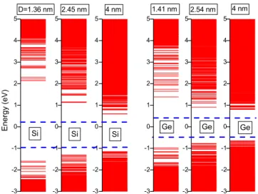
FIG. 2.共Color online兲 The variation of NC states with respect to diameter for Si and Ge NCs. The bulk band edges are marked with a dashed line for comparison.
FIG. 3.共Color online兲 Illustration for the three different absorp-tion processes in NCs considered in this work: interband, intraband, and excited-state absorption. The yellow共light colored兲 arrows in-dicate the direct photon absorption transitions, the blue共dark col-ored兲 arrow represents optical pumping, and the downward green arrow corresponds to luminescence, which can be to an interface state共dashed line兲.
ing several thousand atoms.37,38 The fact that it is a pseudopotential-based method makes it more preferable over the empirical tight binding technique for the study of optical properties, as aimed in this work. In this technique, the NC wave function with a state label j is expanded in terms of the bulk Bloch bands of the constituent core and/or embedding medium共matrix兲 materials,
j共rជ兲 = 1
冑
Nn,kជ,兺
Cn,kជ,j eikជ·rជu n,kជ 共rជ兲, 共1兲 where N is the number of primitive cells within the compu-tational supercell, Cn,kជ,j is the expansion coefficient set to be determined, and is the constituent bulk material label pointing to the NC core or embedding medium. un,kជ 共rជ兲 is the cell-periodic part of the Bloch states, which can be expanded in terms of the reciprocal lattice vectors兵Gជ其 asun,kជ 共rជ兲 = 1 ⍀0
兺
GជBnkជ共Gជ兲eiGជ·rជ, 共2兲 where⍀0 is the volume of the primitive cell. The atomistic Hamiltonian for the system is given by
Hˆ = − ប 2ⵜ2
2m +
兺
,Rជj,␣
W␣共Rជj兲␣共rជ− Rជj− dជ␣兲, 共3兲
where W␣共Rជj兲 is the weight function that takes values 0 or 1
depending on the type of atom at the position Rជj− dជ␣,46 and
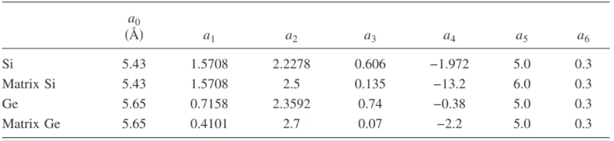
␣is the screened spherical pseudopotential of atom␣of the material . We use semiempirical pseudopotentials for Si and Ge developed particularly for strained Si/Ge
superlat-tices, which reproduces a large variety of measured physical data such as bulk band structures, deformation potentials, electron-phonon matrix elements, and heterostructure va-lence band offsets.47With such a choice, this approach ben-efits from the empirical pseudopotential method 共EPM兲, which in addition to its simplicity has another advantage over the more accurate density functional ab initio tech-niques that run into the well-known band-gap problem,31 which is a disadvantage for the correct prediction of the ex-citation energies.
The formulation can be cast into the following general-ized eigenvalue equation:38,43
兺
n,kជ, Hn⬘kជ⬘⬘,nkជCn,kជ = E兺
n,kជ, Sn⬘kជ⬘⬘,nkជCn,kជ , 共4兲 where Hn⬘kជ⬘⬘,nkជ⬅ 具n⬘
kជ⬘
兩Tˆ + Vˆxtal兩nkជ典, 具n⬘
kជ⬘
兩Tˆ兩nkជ典 =␦kជ⬘,kជ兺
Gជ ប2 2m兩Gជ+ kជ兩 2B n⬘kជ⬘ ⬘ 共Gជ兲*B nkជ 共Gជ兲, FIG. 4.共Color online兲 Comparison of optical gap as a functionof NC diameter of this work with previous experimental and theo-retical data共Refs.10–12,16,22,32,35, and59兲.
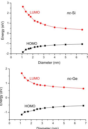
FIG. 5. 共Color online兲 The variation of HOMO and LUMO energies with respect to NC diameter for Si and Ge NCs that belong to the C3vpoint group.
具n
⬘
kជ⬘
兩Vˆxtal兩nkជ典 =兺
Gជ,Gជ Bn⬘⬘kជ⬘共Gជ兲*Bnkជ共Gជ兲 ⫻兺
⬙,␣ V␣⬙共兩Gជ + kជ− Gជ − kជ兩2兲 ⫻W␣⬙共kជ− kជ兲ei共Gជ+kជ−Gជ−kជ兲·dជ␣⬙, Sn⬘kជ⬘⬘,nkជ⬅ 具n⬘
kជ⬘
兩nkជ典.Here, the atoms are on regular sites of the underlying Bravais lattice: Rជn1,n2,n3= n1aជ1+ n2aជ2+ n3aជ3, where 兵aជi其 are its direct
lattice vectors of the Bravais lattice. Both the NC and the host matrix are assumed to possess the same lattice constant and the whole structure is within a supercell, which imposes that the periodicity condition W共Rជn1,n2,n3+ Niaជi兲=W共Rជn1,n2,n3兲, recalling its Fourier representation W共Rជn1,n2,n3兲
→兺W˜ 共q兲eiqជ·Rជn1,n2,n3, implies eiqជ·Niaជi= 1, so that qជ→qជ m1,m2,m3 = bជ1 m1 N1+ b ជ2m2 N2+ b ជ3m3 N3, where兵b
ជi其 are the reciprocal lattice vec-tors of the bulk material. Thus, the reciprocal space of the supercell arrangement is not a continuum but is of the grid form composed of points兵qជm1,m2,m3其, where mi= 0 , 1 , . . . , Ni
− 1.
An important issue is the choice of the host matrix mate-rial. If the NC is surrounded by vacuum, this corresponds to the freestanding case. However, the dangling bonds of the surface NC atoms lead to quite a large number of interface states, which adversely contaminate especially the effective band-gap region of the NC. In practice, NCs are embedded into a wide band-gap host matrix, which is usually silica.45 However, the pseudopotential for oxygen is nontrivial in the case of EPM48and, furthermore, the lattice constant of SiO
2 is not matched to either of the core materials introducing strain effects. Therefore, we embed the Si and Ge NCs into an artificial wide band-gap medium, which for the former reproduces the proper band alignment of the Si/SiO2system. To circumvent the strain effects which are indeed present in the actual samples, we set the lattice constant and crystal structure of the matrix equal to that of the core material. The pseudopotential form factors of the wide band-gap matrices for Si and Ge can easily be produced starting from those of the core materials. More details are provided in the Appen-dix. The resultant bulk band structures for Si and Ge and their host wide band-gap matrices are shown in Fig.1. With the use of such a lattice-matched matrix providing the perfect termination of the surface bonds of the NC core atoms leads FIG. 6.共Color online兲 共a兲 The energy difference between doubly
degenerate and nondegenerate states, one of which becomes the HOMO with respect to diameter in Si and Ge NCs that belong to the C3vpoint group; solid lines are for guiding the eyes; a0is the
lattice constant for Si or Ge NC.共b兲 The lowest three conduction states, one of which becomes the LUMO with respect to diameter in Si NCs.
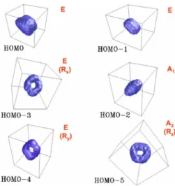
FIG. 7. 共Color online兲 The isosurfaces of the envelopes of the wave functions of the highest-lying six valence states up to HOMO for a Si NC of diameter of 2.16 nm. The isosurfaces are drawn for 95% of the peak value of the envelope wave functions. The C3v
point group representations are indicated for each wave function. Note that some of the plots are rotated with respect to others for best viewing angle.
to the removal of all gap states, as can be observed in Fig.2. In these plots, the evolution of the effective band gaps to-ward their bulk values 共marked by dashed lines兲 is clearly seen as the diameter increases.
Once the electronic wave functions of the NCs are avail-able, their linear optical properties can be readily computed. The three different types of direct共zero phonon兲 photon ab-sorption processes considered in this work are illustrated in Fig.3. These are interband, intraband, and excited-state ab-sorptions. In the latter, the blue共dark colored兲 arrow repre-sents optical pumping and following carrier relaxation, the downward green arrow corresponds to luminescence, which can be to a final interface state共dashed line兲.2 For all these processes, the relevant quantity is the imaginary part of the dielectric function. Within the independent-particle approxi-mation and the artificial supercell framework,17 it becomes
Im兵⑀aa共兲其 = 共2eប兲2 m0VSC
兺
c,v fcvaa Ec− Ev ⌫/共2兲 关Ec− Ev−ប兴2+共⌫/2兲2 , 共5兲 where a = x , y , z denotes the Cartesian components of the di-electric tensor andfcvaa= 2m0
冏
冓
c冏
pa m0冏
v冔
冏
2 Ec− Ev 共6兲 is the oscillator strength of the transition. In these expres-sions, m0is the free electron mass, e is the magnitude of the electronic charge, and ⌫ is the full width at half maximum value of the Lorentzian broadening. The label v 共c兲 corre-spond to occupied共empty兲 valence 共conduction兲 statesrefer-ring only to their orbital parts in the absence of spin-orbit coupling; the spin summation term is already accounted in the prefactor of Eq. 共5兲. Finally, VSC is the volume of the supercell, which is a fixed value chosen conveniently large to accommodate the NCs of varying diameters; however, if one uses instead, that of the NC, VNC, this corresponds calculat-ing Im兵⑀aa其/ fv, where fv= VNC/VSCis the volume filling ratio of the NC. For the sake of generality, this is the form we shall be presenting our results. The electromagnetic intensity absorption coefficient␣共兲 is related to the imaginary part of the dielectric function through49
Im兵⑀aa共兲其 =
nrc
␣aa共兲, 共7兲
where nris the index of refraction and c is the speed of light.
In the case of intraband absorption, its rate depends on the amount of excited carriers. Therefore, we consider the ab-sorption rate for one excited electron or hole that lies at an initial state i with energy Ei. As there are a number of closely
spaced such states, we perform a Boltzmann averaging over these states as e−Ei/兺
je−Ej. We further assume that the final
states have no occupancy restriction, which can easily be relaxed if needed. The expression for the absorption rate per an excited carrier in each NC becomes
␣aa fv = e 2 2m0cnrVNC
兺
i,f e−Ei兺
j e−Ej ffi aa关E f− Ei兴 ⫻ ⌫/共2兲 关Ef− Ei−ប兴2+共⌫/2兲2 , 共8兲where again a is the light polarization direction. TABLE I. C3v irreducible representations of the HOMO and LUMO in Si and Ge NCs of various
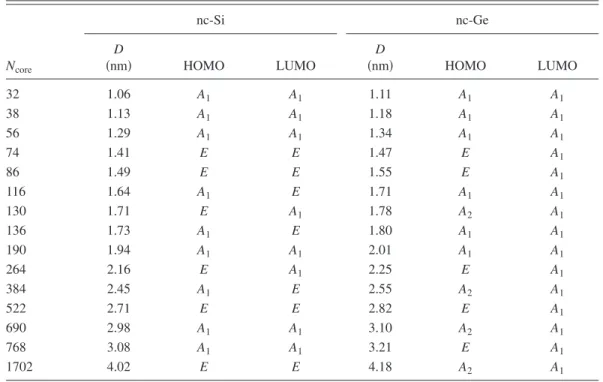
diameters共D兲. Ncore nc-Si nc-Ge D 共nm兲 HOMO LUMO D 共nm兲 HOMO LUMO 32 1.06 A1 A1 1.11 A1 A1 38 1.13 A1 A1 1.18 A1 A1 56 1.29 A1 A1 1.34 A1 A1 74 1.41 E E 1.47 E A1 86 1.49 E E 1.55 E A1 116 1.64 A1 E 1.71 A1 A1 130 1.71 E A1 1.78 A2 A1 136 1.73 A1 E 1.80 A1 A1 190 1.94 A1 A1 2.01 A1 A1 264 2.16 E A1 2.25 E A1 384 2.45 A1 E 2.55 A2 A1 522 2.71 E E 2.82 E A1 690 2.98 A1 A1 3.10 A2 A1 768 3.08 A1 A1 3.21 E A1 1702 4.02 E E 4.18 A2 A1
Finally, we include the surface polarization effects, also called local field effects共LFEs兲 using a simple semiclassical model, which agrees remarkably well with more rigorous treatments.50We give a brief description of its implementa-tion. First, using the expression
⑀SC= fv⑀NC+共1 − fv兲⑀matrix, 共9兲 we extract共i.e., deembed兲 the size-dependent NC dielectric function⑀NC, where⑀SCcorresponds to Eq. 共5兲, suppressing the Cartesian indices.⑀matrixis the dielectric function of the host matrix; for simplicity, we set it to the permittivity value of SiO2, i.e.,⑀matrix= 4. Since the wide band-gap matrix in-troduces no absorption up to an energy of about 9 eV, we can approximate Im兵⑀NC其=Im兵⑀SC其/ fv. One can similarly
ob-tain Re兵⑀NC其 within the random phase approximation,23 hence get the full complex dielectric function⑀NC. According to the classical Clausius-Mossotti approach, which is shown to work also for NCs,51 the dielectric function of the NC is modified as
⑀NC,LFE=⑀matrix
冋
4⑀NC−⑀matrix ⑀NC+ 2⑀matrix
册
, 共10兲
to account for LFE. The corresponding supercell dielectric function⑀SC,LFEfollows using Eq.共9兲. Similarly, the intensity
absorption coefficients are also modified due to surface
po-larization effects, cf. Eq. 共7兲. Its consequences will be
re-ported in Sec. IV.
III. SELF-CRITIQUE OF THE THEORETICAL MODEL
The most crucial simplification of our model is the fact that strain-related effects are avoided, a route which is shared by other theoretical works.17,18,23,35,52 For large NCs, this may not be critical; however, for very small sizes, this sim-plification is questionable. An important support for our act is that Weissker et al. have concluded that while there is some shift and possibly a redistribution of oscillator strengths after ionic relaxation, the overall appearance of the absorption spectra does not change strongly.19 We should mention that Wang and Zunger have offered a recipe for including strain within the LCBB framework; however, this is considerably more involved.38Another widespread simpli-fication on Si and Ge NCs is the omission of the spin-orbit coupling and the nonlocal 共angular momentum dependent兲 pseudopotential terms in the electronic structure Hamil-tonian. Especially, the former is not significant for Si which is a light atom but it can have a quantitative impact on the valence states of Ge NCs; such a treatment is available in Ref.53.
On the dielectric response, there are much more sophisti-cated and involved treatments,54 whereas ours is equivalent FIG. 8. 共Color online兲 The imaginary part of dielectric function for unity volume filling factor,
fvfor Si and Ge NCs at different diameters with
共right panel兲 and without 共left panel兲 local field effects. A Lorentzian broadening energy width of 200 meV is used.
to the independent-particle random phase approximation55of the macroscopic dielectric function with the surface polariza-tion effects included within the classical Clausius-Mossotti model.50 The contribution of the excluded excitonic and other many-body effects beyond the mean-field level can be assessed a posteriori by comparing with the available experi-mental data. However, it is certain that the precedence should be given to classical electrostatics for properly describing the background dielectric mismatch between the core and the wide band-gap matrix.50 In our treatment, this is imple-mented at an atomistic level.
Another effect not accounted in this work is the role of the interface region. Our wide band-gap matrix can reproduce the proper band alignment and dielectric confinement of an SiO2 matrix; however, the interface chemistry such as silicon-oxygen double bonds7is not represented. These were shown to be much more effective on the emission spectra.6,7 Nevertheless, our results can be taken as the benchmark for the performance of the atomistic quantum and dielectric con-finement with a clean and inert interface. Finally, we do not consider the phonon-assisted56 or nonlinear absorption. The list of these major simplifications also suggests possible im-provements of this work.
IV. RESULTS AND DISCUSSIONS
In this section, we present our theoretical investigation of the linear optical properties of Si and Ge NCs. Three differ-ent direct photon absorption processes are considered, as il-lustrated in Fig.3, each of which can serve for technological applications as well as to our basic understanding. However, we first begin with the dependence of the optical gap on the NC size, mainly as a check of our general framework. There exist two different atomic arrangements of a spherical NC depending on whether the center of the NC is an atomic position or a tetrahedral interstitial location; under no ionic relaxation, Delley and Steigmeier have treated both of these classes as having the Tdpoint symmetry.52However, the
tet-rahedral interstitial-centered arrangement should rather have
the lower point symmetry of C3v and it is the arrangement
that we construct our NCs. This leads to the even number of NC core atoms, whereas it becomes an odd number with the Tdpoint symmetry. We identify the irreducible representation
of a chosen NC state by checking its projection to the sub-space of each representation.57For the C
3vpoint group, these
are denoted by A1, A2, and E. We utilize this group-theoretic analysis in the next subsections.
FIG. 9.共Color online兲 The local field absorption factor extracted from the previous figure.
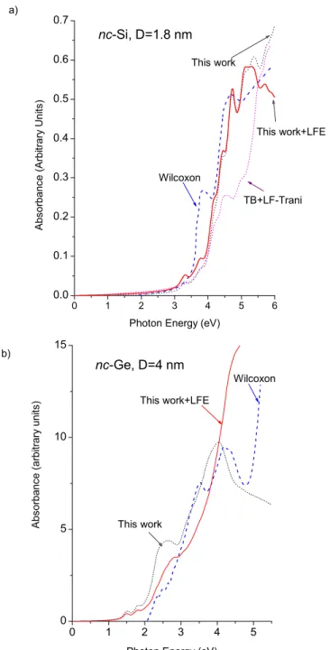
FIG. 10. 共Color online兲 Comparison of our absorbance results with the available data: for Si, experimental work of Wilcoxon et al. 共Ref. 13兲 and the theoretical tight binding results of Trani et al.
共Ref. 50兲, and for Ge, the experimental work of Wilcoxon et al.
共Ref.15兲. For our spectra, a Lorentzian broadening energy width of
A. Effective optical gap
The hallmark of quantum size effect in NCs has been the effective optical gap with quite a number of theoretical16,22,23,32,58,59 and experimental11–13,15 studies per-formed within the last decade. Figure4 contains a compila-tion of some representative results. For Si NCs, it can be observed that there is a good agreement among the existing data, including ours. On the other hand, for the case of Ge NCs, there is a large spread between the experimental data, whereas our theoretical results are in very good agreement with both ab initio22 and tight binding results.23 In our ap-proach, the optical gap directly corresponds to the lowest unoccupied molecular orbital–highest occupied molecular orbital共LUMO-HOMO兲 energy difference, as calculated by the single-particle Hamiltonian in Eq. 共3兲. This simplicity
relies on the finding of Delerue et al. that the self-energy and Coulomb corrections almost exactly cancel each other for Si NCs larger than a diameter of 1.2 nm.60
B. Highest occupied molecular orbital and lowest unoccupied molecular orbital oscillations with respect to size
When we plot the variation of individual LUMO and HOMO levels as in Fig.5, we observe with the exception of nc-Ge LUMO curve some nonsmooth behavior that gets pro-nounced toward smaller sizes. The triple degeneracy in the absence of spin-orbit coupling of the valence band maximum in bulk Si and Ge is lifted into two degenerate and one non-degenerate states. The energy difference between these two sets of states is observed to display an oscillatory behavior as the NC size gets smaller, as shown in Fig. 6共a兲. Using the C3vpoint group symmetry operations, we identify the doubly
degenerate states to belong to E representation and
nonde-generate state to A1or A2. Furthermore, we observe a similar oscillation in the LUMO region of Si NCs, as shown in Fig.
6共b兲. The low-lying conduction states of Si NCs form six-pack groups, which is inherited from the six equivalent 0.85X conduction band minima of bulk Si. The confinement marginally lifts the degeneracy by sampling contributions from other parts of the Brillouin zone. This trend is observed in Fig.6共b兲as the NC size gets smaller. On the other hand, for Ge NCs, all LUMO states belong to the same A1 repre-sentation and therefore show no oscillations共cf. Fig.5兲.
Ul-timately, the source of these oscillations is the variation of the asphericity of the NCs of C3v point symmetry with re-spect to size, which can energetically favor one of the closely spaced states. In the case of the LUMO state of Ge NCs, there is a substantial energy gap between LUMO and the next higher-lying state.
For further insight, we display in Fig. 7 the isosurface plots of the envelope of the six highest states up to HOMO for a Si NC of diameter 2.16 nm. Point group representation of each state is also indicated. For this particular diameter, HOMO has E representation, which is twofold degenerate. The nondegenerate A1 state also becomes the HOMO for different diameters. This is illustrated in Table I, which shows the evolution of the HOMO and LUMO symmetries as a function of diameter for Si and Ge NCs. There, it can be observed that for the latter, the HOMO can also acquire the A2 for larger diameters.
C. Interband absorption
The interband absorptions of Si and Ge NCs for a variety of diameters are shown in Fig.8. For a fair comparison, all different size NCs should possess the same volume filling factor. Therefore, we display the results at unity volume fill-ing or equivalently per fv.18The left and right panels display
the cases without and with surface polarization effects 共or LFE兲, respectively. There exist remarkable differences be-tween the two for both Si and Ge NCs. For instance, even though Ge NCs do not show significant size dependence without LFE, this is not the case when LFE is included. From the ratio of both panels, the so-called local field ab-sorption reduction factor can be extracted, as shown in Fig.
9. It can be observed that its size dependence is much stron-ger than the energy dependence. This reduction in the ab-sorption due to LFE can become a major concern for solar cell applications. It needs to be mentioned that this effect is highly sensitive to the permittivity mismatch between the core and matrix media. To illustrate this point, in Fig.9, the case for Al2O3 matrix共having a permittivity of 9.1兲 is also displayed for 1.41 nm Si NC, where it can be seen that com-pared to SiO2共with a permittivity of about 4兲, the reduction in absorption due to LFE is much less. Based on this finding, we employ these size-dependent absorption reduction factors in the results to follow including the intraband and excited-state cases.
In Fig.10, we compare our results with the experimental data of Wilcoxon et al. for Si NCs13and Ge NCs.15There is a good overall agreement in both cases especially with LFE; however, for the case of Si NCs, this is much more satisfac-FIG. 11. 共Color online兲 The effect of ellipticity e on the
Im兵⑀zz其/ fv for a Ge NC with a diameter of 2.54 nm. The insets
show NC core atoms of the prolate共e=−0.6兲 and oblate 共e=0.6兲 shapes; the z direction is also indicated. A Lorentzian broadening energy width of 200 meV is used.
tory. The major discrepancies can be attributed to excitonic effects that are not included in our work. In the case of Si NCs关Fig.10共a兲兴, we also display the tight binding result of Trani et al., which also includes LFE.50
An issue of practical concern is the effect of deviation from the spherical shape of the NCs depending on the growth conditions. At this point, we would like to investigate the effect of shape anisotropy on the interband absorption. Starting from a spherical 2.54 nm diameter Ge NC, we form prolate and oblate ellipsoidal NCs with ellipticities e = −0.6 and +0.6, respectively. All three NCs contain the same num-ber of 384 core atoms; the atomic arrangement of the ellip-soidal NCs are shown in the inset of Fig. 11. In the same figure, we compare the zz components of the imaginary part of the dielectric tensor for three different ellipticities. It is observed that the effect on the interband absorption is not significant; the difference is even less for the Si NCs 共not shown兲.
D. Intraband absorption
Unlike the interband case, for the intraband absorption, we need to introduce electrons to the conduction states or
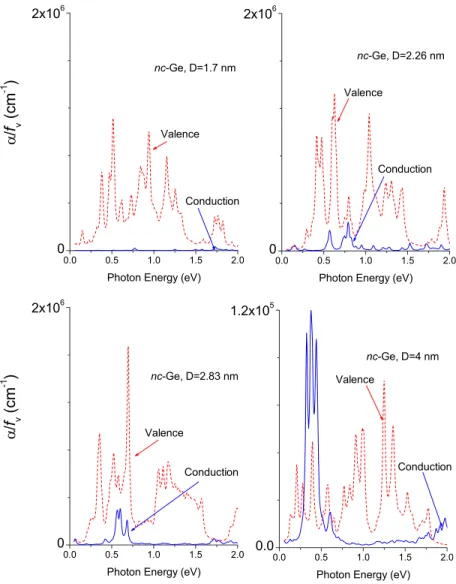
holes to the valence states by an injection mechanism. We assume that after injection, these carriers relax to their re-spective band edges and attain a thermal distribution. There-fore, we perform a Boltzmann averaging at room tempera-ture共300 K兲 over the initial states around LUMO 共HOMO兲 for electrons 共holes兲. The absorption coefficients to be pre-sented are for unity volume filling factors and for one carrier per NC; they can easily be scaled to a different average num-ber of injected carriers and volume filling factors. In Fig.12, the Si NCs of different diameters are compared. The intra-band absorption is observed to be enhanced as the NC size grows up to about 3 nm followed by a drastic fall for larger sizes. For both holes and electrons, a very large number of absorption peaks are observed from 0.5 to 2 eV. Recently, de Sousa et al. have also considered the intraband absorption in Si NCs using the effective mass approximation and taking into account the multivalley anisotropic band structure of Si.61 However, their absorption spectra lacks much of the features seen in Fig.12. Turning to Ge NCs, shown in Fig.
13, the intravalence band absorption profile is very similar to that of Si NCs; however, in this, case the intraconduction band absorption is much weaker.
Mimura et al. have measured the optical absorption in heavily phosphorus doped Si NCs of a diameter of 4.7 nm.62 FIG. 12. 共Color online兲 Intravalence and in-traconduction state absorption coefficients in Si NCs of different diameters per excited carrier and at unity filling factor. A Lorentzian broadening energy width of 30 meV is used. Mind the change in the vertical scale for the 4 nm diameter case.
This provides us an opportunity to compare our results on the intraconduction band absorption in Si NCs. There is a good order-of-magnitude agreement. However, in contrast to our spectra in Fig. 12 which contains well-resolved peaks, they have registered a smooth spectrum, which has been at-tributed by the authors to the smearing out due to size and shape distribution within their NC ensemble.62
E. Excited-state absorption
Finally, we consider another intraband absorption process where the system is under a continuous interband optical
pumping that creates electrons and holes with excess energy. We consider three different excitation wavelengths, 532, 355, and 266 nm, which, respectively, correspond to the second, third, and fourth harmonics of the neodymium-doped yttrium aluminum garnet 共Nd:YAG兲 laser at 1064 nm. The initial states of the carriers after optical pumping are chosen to be at the pair of states with the maximum oscillator strength44 among interband transitions under the chosen excitation. The determined energies of these states are tabulated in TableII, where it can be observed that, in general, the excess energy is unevenly partitioned, mainly in favor of the conduction states. Once again, a Boltzmann averaging is used to get the
TABLE II. The excited-state energies of the carriers within the valence and conduction states under three different interband pump energies for nc-Si and nc-Ge. The energies are given in eV and measured from the HOMO and LUMO, respectively.
Pump nc-Si nc-Ge D = 3 nm D = 4 nm D = 3 nm D = 4 nm 2.33 0.197, 0.021 0.021, 0.551 0.103, 0.643 0.211, 0.663 3.50 0.000, 1.432 0.316, 1.440 0.400, 1.508 1.141, 0.892 4.66 0.188, 2.414 0.713, 2.218 0.511, 2.551 1.360, 1.853
FIG. 13. 共Color online兲 Same as Fig.12 but for Ge NCs.
contribution of states within the thermal energy neighbor-hood.
Considering 3 and 4 nm diameters, the results are shown in Figs.14and15for Si and Ge NCs, respectively. Note that the 532 nm excitation results are qualitatively similar to those in intraband absorption, cf. Figs. 12 and 13. This is expected on the grounds of small excess energy for this case. Some general trends can be extracted from these results. First of all, the conduction band absorption is, in general, smooth over a wide energy range. On the other hand, the valence band absorption contains pronounced absorption at several narrow energy windows mainly below 1 eV and they get much weaker than the conduction band absorption in the remaining energies. As the excitation energy increases, the absorption coefficient per excited carrier, in general, de-creases. In connection to silicon photonics, we should point out that the excited-state absorption is substantial including the important 1.55m fiber optics communication wave-length. These results provide a more comprehensive picture than the reported experimental measurements,27–29which are
usually obtained at a single energy of the probe beam. Fi-nally, it needs to be mentioned that for both intraband and excited-state absorptions displayed in Figs. 12–15, the high energy parts will be masked by the interband transition whenever it becomes energetically possible.
V. CONCLUSIONS
The subject of Si and Ge NCs has become an established research field. A fundamental process such as the direct pho-ton absorption deserves further investigation from a number of perspectives. In this theoretical study, we consider the interband, intraband, and excited-state absorption in embed-ded Si and Ge NCs of various sizes. For this purpose, we developed an atomistic pseudopotential electronic structure tool, the results of which agree very well with the published data. It is further observed that the HOMO for both Si and Ge NCs and the LUMO for Si NCs display oscillations with respect to size among different representations of the C3v point group to which these spherical NCs belong. Our de-FIG. 14. 共Color online兲 Excited-state absorption within valence and conduction states of Si NCs per excited carrier and at unity filling factor under three dif-ferent optical pumping wave-lengths of 532, 355, and 266 nm. Dotted lines in black color refer to total absorption coefficients. Two different diameters are considered, 3 and 4 nm. A Lorentzian broad-ening energy width of 30 meV is used.
tailed investigation of the interband absorption reveals the importance of surface polarization effects that significantly reduce the absorption when included. This reduction is found to increase with decreasing NC size or with increasing per-mittivity mismatch between the NC core and the host matrix. These findings should be taken into account for applications where the absorption is desired to be either enhanced or re-duced. For both NC types, the deviation from sphericity shows no pronounced effect on the interband absorption. Next, the intraband process is considered, which has poten-tial applications on mid- and near-infrared photodetection. The intravalence band absorption is stronger compared to the intraconduction band especially below 1 eV. Finally, we demonstrate that optical pumping introduces a new degree of freedom to intraband absorption. This is studied under the title of excited-state absorption. Our major finding is that the excited-state absorption is substantial including the impor-tant 1.55m fiber optics communication wavelength. Within the context of achieving gain and lasing in these NCs, excited-state absorption is a parasitic process; however, it
can acquire a positive role in a different application.
ACKNOWLEDGMENTS
The author is grateful to Aykutlu Dâna for his suggestion of the intersubband absorption and its photodetector applica-tions. This work has been supported by the European FP6 Project SEMINANO with Contract No. NMP4 CT2004 505285 and by the Turkish Scientific and Technical Council TÜBİTAK with Project No. 106T048. The computational re-sources are supplied in part by TÜBİTAK through TR-Grid e-Infrastructure Project.
APPENDIX: SOME TECHNICAL DETAILS ON THE LINEAR COMBINATION OF BULK BAND
IMPLEMENTATION
In this section, we first provide the details on the pseudo-potential form factors of the bulk Si, Ge, and their associated wide band-gap matrices to substitute for SiO2. We use the FIG. 15. 共Color online兲 Same as Fig.14but for Ge NCs.
local empirical pseudopotentials for Si and Ge developed by Friedel et al.47 They use the following functional form for the pseudopotential form factor at a general wave number q:
VPP共q兲 = a1共q 2− a 2兲 ea3共q2−a4兲+ 1
冋
1 2 tanh冉
a5− q2 a6冊
+1 2册
. Using the parameters supplied in TableIII, the pseudopoten-tial form factors come out in Rydbergs and the wave number in the above equation should be taken in atomic units 共1/ Bohr radius兲. Another important technical remark is about the EPM cutoff energies. We observed that even though the EPM band energies共i.e., eigenvalues兲 converge reasonably well with cut off energies as low as 5 – 10 Ry, the corre-sponding Bloch functions 共i.e., eigenvectors兲 requiresub-stantially higher values to converge.63 The results in this study are obtained using 14 and 16 Ry for Si and Ge, respec-tively.
Finally, some comments on the LCBB basis set construc-tion are in order. We only employ the bulk bands of the core material. The bulk band indices are chosen from the four valence bands and the lowest three to four conduction bands; usually, these are not used in conjunction but separately for the NC valence and conduction states, respectively. The basis set is formed from a sampling over a three-dimensional rect-angular grid in the reciprocal space centered around the ⌫ point. Its extend is decided by the significant band extrema, such as conduction band minima of Si at the six equivalent 0.85X points. The final LCBB basis set typically contains some 10 000 members.
1S. Ossicini, L. Pavesi, and F. Priolo, Light Emitting Silicon for Microphotonics共Springer-Verlag, Berlin, 2004兲.
2L. Pavesi, L. Dal Negro, C. Mazzoleni, G. Franzó, and F. Priolo,
Nature共London兲 408, 440 共2000兲.
3R. J. Walters, G. I. Bourianoff, and H. A. Atwater, Nat. Mater. 4,
143共2005兲.
4H. Rong, A. Liu, R. Jones, O. Cohen, D. Hak, A. Fang, and M.
Paniccia, Nature共London兲 433, 292 共2005兲; H. Rong, R. Jones, A. Liu, O. Cohen, D. Hak, A. Fang, and M. Paniccia, ibid. 433, 725共2005兲.
5M. V. Wolkin, J. Jorne, P. M. Fauchet, G. Allan, and C. Delerue,
Phys. Rev. Lett. 82, 197共1999兲.
6Z. Zhou, L. Brus, and R. Friesner, Nano Lett. 3, 163共2003兲. 7M. Luppi and S. Ossicini, Phys. Rev. B 71, 035340共2005兲. 8I. Sagnes, H. Halimaoui, G. Vincent, and P. A. Badoz, Appl. Phys.
Lett. 62, 1155共1993兲.
9M. Green, Third Generation Photovoltaics共Springer-Verlag,
Ber-lin, 2006兲.
10S. Furukawa and T. Miyasato, Phys. Rev. B 38, 5726共1988兲. 11Y. Kanemitsu, H. Uto, Y. Masimoto, and Y. Maeda, Appl. Phys.
Lett. 61, 2187共1992兲.
12S. Takeoka, M. Fujii, S. Hayashi, and K. Yamamoto, Phys. Rev. B
58, 7921共1998兲.
13J. P. Wilcoxon, G. A. Samara, and P. N. Provencio, Phys. Rev. B
60, 2704共1999兲.
14D. Kovalev, J. Diener, H. Heckler, G. Polisski, N. Künzner, and
F. Koch, Phys. Rev. B 61, 4485共2000兲.
15J. P. Wilcoxon, P. P. Provencio, and G. A. Samara, Phys. Rev. B
64, 035417共2001兲.
16I. Vasiliev, S. Öğüt, and J. R. Chelikowsky, Phys. Rev. Lett. 86,
1813共2001兲.
17H.-Ch. Weissker, J. Furthmüller, and F. Bechstedt, Phys. Rev. B
65, 155327共2002兲.
18H.-Ch. Weissker, J. Furthmüller, and F. Bechstedt, Phys. Rev. B
65, 155328共2002兲.
19H.-Ch. Weissker, J. Furthmüller, and F. Bechstedt, Phys. Rev. B
67, 245304共2003兲.
20L. E. Ramos, H.-Ch. Weissker, J. Furthmüller, and F. Bechstedt,
Phys. Status Solidi B 242, 3053共2005兲.
21D. V. Melnikov and J. R. Chelikowsky, Solid State Commun.
127, 361共2003兲; Phys. Rev. B 69, 113305 共2004兲.
22A. Tsolakidis and R. M. Martin, Phys. Rev. B 71, 125319共2005兲. 23F. Trani, G. Cantele, D. Ninno, and G. Iadonisi, Phys. Rev. B 72,
075423共2005兲.
24Y.-Y. Lin and J. Singh, J. Appl. Phys. 96, 1059共2004兲.
25V. Ryzhii, I. Khmyrova, V. Mitin, M. Stroscio, and M. Willander,
Appl. Phys. Lett. 78, 3523共2001兲.
26A. V. Malko, A. A. Mikhailovsky, M. A. Petruska, J. A.
Holling-sworth, and V. I. Klimov, J. Phys. Chem. B 108, 5250共2004兲.
27R. G. Elliman, M. J. Lederer, N. Smith, and B. Luther-Davies,
Nucl. Instrum. Methods Phys. Res. B 206, 427共2003兲.
28F. Trojánek, K. Neudert, M. Bittner, and P. Malý, Phys. Rev. B
72, 075365共2005兲.
29M. Forcales, N. J. Smith, and R. G. Elliman, J. Appl. Phys. 100,
014902共2006兲.
TABLE III. Parameters of the pseudopotential form factors of Si, Ge, and their wide band-gap matrices.
a0is the lattice constant共see text for the units兲.
a0 共Å兲 a1 a2 a3 a4 a5 a6 Si 5.43 1.5708 2.2278 0.606 −1.972 5.0 0.3 Matrix Si 5.43 1.5708 2.5 0.135 −13.2 6.0 0.3 Ge 5.65 0.7158 2.3592 0.74 −0.38 5.0 0.3 Matrix Ge 5.65 0.4101 2.7 0.07 −2.2 5.0 0.3
30A. Zunger, Phys. Status Solidi A 190, 467共2002兲.
31R. M. Martin, Electronic Structure共Cambridge University Press,
Cambridge, 2004兲.
32S. Öğüt, J. R. Chelikowsky, and S. G. Louie, Phys. Rev. Lett. 79,
1770共1997兲.
33C. Delerue and M. Lannoo, Nanostructures: Theory and Model-ling共Springer-Verlag, Berlin, 2004兲.
34S. Y. Ren, Phys. Rev. B 55, 4665共1997兲; S. Y. Ren, Solid State
Commun. 102, 479共1997兲.
35Y. M. Niquet, G. Allan, C. Delerue, and M. Lannoo, Appl. Phys.
Lett. 77, 1182共2000兲.
36L.-W. Wang and A. Zunger, J. Chem. Phys. 100, 2394共1994兲. 37L.-W. Wang, A. Franceschetti, and A. Zunger, Phys. Rev. Lett.
78, 2819共1997兲.
38L.-W. Wang and A. Zunger, Phys. Rev. B 59, 15806共1999兲. 39D. Ninno, K. B. Wong, M. A. Gell, and M. Jaros, Phys. Rev. B
32, 2700共1985兲.
40D. Ninno, M. A. Gell, and M. Jaros, J. Phys. C 19, 3845共1986兲. 41S. Botti and L. C. Andreani, Phys. Rev. B 63, 235313共2001兲. 42S. Botti, N. Vast, L. Reining, V. Olevano, and L. C. Andreani,
Phys. Rev. B 70, 045301共2004兲.
43F. Chirico, A. DiCarlo, and P. Lugli, Phys. Rev. B 64, 045314
共2001兲.
44C. Bulutay, Physica E共Amsterdam兲 38, 112 共2007兲.
45F. Iacona, G. Franzó, and C. Spinella, J. Appl. Phys. 87, 1295
共2000兲.
46An intermediate value between 0 and 1 can be used for the alloys
or modeling the interface region. However, in this work, we set them to either 1 or 0.
47P. Friedel, M. S. Hybertsen, and M. Schlüter, Phys. Rev. B 39,
7974共1989兲.
48J. R. Chelikowsky, Solid State Commun. 22, 351共1977兲. 49J. D. Jackson, Classical Electrodynamics, 2nd ed. 共Wiley, New
York, 1975兲.
50F. Trani, D. Ninno, and G. Iadonisi, Phys. Rev. B 75, 033312
共2007兲.
51G. D. Mahan, Phys. Rev. B 74, 033407共2006兲.
52B. Delley and E. F. Steigmeier, Phys. Rev. B 47, 1397共1993兲. 53F. A. Reboredo and A. Zunger, Phys. Rev. B 63, 235314共2001兲. 54G. Onida, L. Reining, and A. Rubio, Rev. Mod. Phys. 74, 601
共2002兲.
55H. Ehrenreich and M. H. Cohen, Phys. Rev. 115, 786共1959兲. 56M. S. Hybertsen, Phys. Rev. Lett. 72, 1514共1994兲.
57F. A. Reboredo, A. Franceschetti, and A. Zunger, Phys. Rev. B
61, 13073共2000兲.
58L.-W. Wang and A. Zunger, J. Phys. Chem. 98, 2158共1994兲. 59C. S. Garoufalis, A. D. Zdetsis, and S. Grimme, Phys. Rev. Lett.
87, 276402共2001兲.
60C. Delerue, M. Lannoo, and G. Allan, Phys. Rev. Lett. 84, 2457
共2000兲.
61J. S. de Sousa, J.-P. Leburton, V. N. Freire, and E. F. da Silva, Jr.,
Appl. Phys. Lett. 87, 031913共2005兲.
62A. Mimura, M. Fujii, S. Hayashi, D. Kovalev, and F. Koch, Phys.
Rev. B 62, 12625共2000兲.