NANOTRIBOLOGICAL PROPERTIES OF
GRAPHENE GROWN BY CHEMICAL
VAPOR DEPOSITION AND TRANSFERRED
ONTO SILICON OXIDE SUBSTRATES
A THESIS SUBMITTED TO
THE GRADUATE SCHOOL OF ENGINEERING AND SCIENCE OF BILKENT UNIVERSITY
IN PARTIAL FULFILLMENT OF THE REQUIREMENTS FOR THE DEGREE OF MASTER OF SCIENCE IN MECHANICAL ENGINEERING
By
Tuna Demirbaş
October, 2015
ii
NANOTRIBOLOGICAL PROPERTIES OF GRAPHENE GROWN BY CHEMICAL VAPOR DEPOSITION AND TRANSFERRED ONTO SILICON OXIDE SUBSTRATES
By Tuna Demirbaş October, 2015
We certify that we have read this thesis and that in our opinion it is fully adequate, in scope and in quality, as a thesis for the degree of Master of Science.
Assist. Prof. Dr. Mehmet Zeyyad Baykara (Advisor)
Assist. Prof. Dr. Yegân Erdem
Assoc. Prof. Dr. Erdem Alaca
Approved for the Graduate School of Engineering and Science:
Prof. Dr. Levent Onural Director of the Graduate School
iii
ABSTRACT
NANOTRIBOLOGICAL PROPERTIES OF GRAPHENE
GROWN BY CHEMICAL VAPOR DEPOSITION AND
TRANSFERRED ONTO SILICON OXIDE SUBSTRATES
Tuna Demirbaş
M.S. in Mechanical Engineering
Advisor: Assist. Prof. Dr. Mehmet Zeyyad Baykara
October, 2015
To extend the lifespan of mechanical systems, wear and friction must be minimized with the utilization of lubricants. On the other hand, traditional fluid-based lubrication schemes fail in nano- and micro-scale systems due to increasing surface-to-volume ratios and associated physical effects. As such, research efforts in recent years have been aimed at characterizing the structure and mechanical properties of various candidates for solid lubricants.
Due to its outstanding electronic and mechanical properties, the two-dimensional “wonder material” graphene has been the focus of a large variety of experiments in the past decade. Based on its promise as a single-layer solid lubricant suitable for use in nano- and micro-scale systems, the nanotribological properties of graphene have been investigated in several studies in the literature. While frictional characteristics of mechanically exfoliated graphene samples as a function of layer number have been related to the effect of puckering, the nanotribological behavior of graphene samples grown by chemical vapor deposition (CVD) is still under investigation. Considering that high quality graphene of sufficient dimensions for practical applications is currently grown by CVD and requires transfer from metal foils onto various substrates, the need for an extensive understanding of the nanotribological properties of such graphene samples arises.
iv
Based on the discussion above, this M.S. thesis presents a comprehensive structural and nanotribological characterization of CVD-grown graphene transferred onto oxidized silicon substrates (SiO2/Si). In particular, the processes of sample preparation
and post-preparation transfer onto SiO2/Si substrates are optimized via a series of
experiments. Advanced microscopy techniques are utilized for the structural and morphological characterization of the obtained graphene films. In particular, optical microscopy, scanning electron microscopy (SEM), and atomic force microscopy (AFM) are used to inspect graphene coverage on the substrate and associated structural features. On the other hand, Raman spectroscopy is employed to confirm the single-layer character of CVD-grown samples.
The nanotribological properties of CVD-grown graphene samples on SiO2/Si are
studied by AFM in the friction force microscopy (FFM) mode under ambient conditions by measuring the evolution of friction force with increasing normal load. The effect of using different probe tips, growth conditions, and post-transfer cleaning procedures on frictional behavior is evaluated. A comparison of lubrication performance with mechanically-exfoliated graphene is also performed. Results indicate that CVD-grown graphene acts as a very good solid lubricant on SiO2/Si,
reducing coefficients of friction by ~90% for all investigated samples. It is shown that as-transferred CVD-grown graphene exhibits the highest mean lubrication performance and that the associated values drop slightly with post-transfer cleaning. Finally, the effect of wrinkles associated with CVD-grown graphene on measured friction values are quantitatively evaluated, with results revealing a substantial increase in friction on these structural defects.
Keywords: Graphene, Nanotribology, Chemical vapor deposition, Atomic force
v
ÖZET
KİMYASAL BUHAR BİRİKTİRME YÖNTEMİYLE
BÜYÜTÜLEN VE SİLİSYUM OKSİT ALTTAŞ ÜZERİNE
TRANSFER EDİLEN GRAFENİN NANOTRİBOLOJİK
ÖZELLİKLERİ
Tuna Demirbaş
Makine Mühendisliği, Yüksek Lisans
Tez Danışmanı: Yrd. Doç. Dr. Mehmet Zeyyad Baykara
Ekim, 2015
Mekanik sistemlerin ömürlerini uzatmak amacıyla, sürtünme ve aşınma, kayganlaştırıcı malzeme kullanımı ile azaltılmalıdır. Öte yandan, artan yüzey-hacim oranları ve ilgili fiziksel etkiler sebebiyle, sıvı temelli geleneksel yağlama yaklaşımları, nano- ve mikro-boyutlu sistemler için başarılı olmamaktadır. Bu sebeple, geçtiğimiz yıllarda araştırma çalışmaları bir takım katı kayganlaştırıcı adayının yapısal ve mekanik karakterizasyonuna yönelmiştir.
Sahip olduğu sıra dışı elektronik ve mekanik özellikler sebebiyle, iki boyutlu “mucize malzeme” grafen, geçtiğimiz on yıl içerisinde birçok farklı deneyin hedefinde yer almıştır. Nano- ve mikro-boyutlu sistemlerde kullanıma uygun, tek katmanlı katı bir kayganlaştırıcı potansiyeli sergilemesi sebebiyle, grafenin nanotribolojik özellikleri literatürde bulunan bir grup çalışma vasıtasıyla incelenmiştir. Mekanik soyma yöntemi ile elde edilmiş grafenin katman sayısına bağlı sürtünme karakteristikleri buruşma etkisi ile ilişkilendirilmiş olsa da, kimyasal buhar biriktirme (KBB) yöntemi ile büyütülmüş grafen numunelerin nanotribolojik davranışı halen incelenmektedir. Pratik uygulamalar için yeterli boyuta sahip, yüksek kaliteli grafenin hâlihazırda KBB yöntemi ile büyütüldüğü ve metal folyolardan çeşitli alttaşlara transferinin gerektiği göz önüne alındığında, bu tarz grafen numunelerin nanotribolojik özelliklerinin etraflıca anlaşılmasına yönelik bir ihtiyaç ortaya çıkmaktadır.
vi
Yukarıdaki tartışmadan yola çıkarak, bu yüksek lisans tezi, KBB ile büyütülmüş ve oksitlenmiş silisyum alttaşlara (SiO2/Si) transfer edilmiş grafene yönelik kapsamlı bir
yapısal ve nanotribolojik karakterizasyon çalışması sunmaktadır. Bilhassa, bir dizi deney vasıtasıyla, numune hazırlama ve ardından gerçekleşen SiO2/Si üzerine transfer
süreçleri en iyileştirilmiştir. Elde edilen grafen filmlerin yapısal ve morfolojik karakterizasyonu için ileri mikroskopi teknikleri kullanılmıştır. Özellikle, grafenin alttaş üzerindeki kapsama miktarı ve ilgili yapısal özellikler; optik mikroskopi, taramalı elektron mikroskopisi ve atomik kuvvet mikroskopisi (AKM) ile incelenmiştir. KBB ile büyütülmüş numunelerin tek-katman karakterini onaylamak amacıyla, Raman spektroskopisi kullanılmıştır.
KBB ile büyütülmüş grafen numunelerin SiO2/Si üzerinde sergiledikleri
nanotribolojik özellikler; sürtünme kuvvet mikroskopisi (SKM) modunda çalışan AKM ile ortam koşulları altında, sürtünme kuvvetinin artan normal yükle değişimini ölçerek belirlenmiştir. Değişik uç kullanımının, numune büyütme koşullarının ve transfer sonrası temizleme prosedürlerinin sürtünme davranışına olan etkileri değerlendirilmiştir. Bunun haricinde, mekanik soyma ile elde edilen grafen numunelerle kayganlaştırma performansına yönelik bir karşılaştırma da gerçekleştirilmiştir. Sonuçlar, incelenen tüm numuneler için, KBB ile büyütülmüş grafenin SiO2/Si üzerinde çok iyi bir kayganlaştırıcı görevi gördüğünü ve sürtünme
katsayısı değerlerini ~90% seviyesinde azalttığını göstermiştir. KBB ile büyütülmüş grafenin, transfer edilmiş haliyle en yüksek ortalama kayganlaştırma performansını sergilediği ve ilgili değerlerin transfer sonrası temizlemeyle ufak bir miktar düştüğü gösterilmektedir. Son olarak, KBB ile büyütülmüş grafende bulunan kırışıkların ölçülen sürtünme değerleri üzerine etkisi sayısal olarak değerlendirilmiş, sonuçlar bahsi geçen yapısal kusurlar üzerinde sürtünme değerlerinin önemli miktarda arttığını ortaya çıkarmıştır.
Anahtar Kelimeler: Grafen, Nanotriboloji, Kimyasal buhar biriktirme, Atomik kuvvet
vii
Acknowledgement
First of all, I would like express my gratitude to my academic advisor, Prof. Mehmet Zeyyad Baykara, for his unending support and guidance which enabled me to finish my dissertation, as well as giving me an opportunity to be in his research group. Without his presence and knowledge I would have never been able to complete my research and this dissertation. He has been a great, caring, patient and creative professor who has taught me a lot.
Furthermore, I am deeply thankful to the Faculty of Engineering of Bilkent University and the National Nanotechnology Research Center (UNAM) administrators who provided an excellent scientific environment, as well as the necessary tools and materials for my studies. I will never forget all the technicians at UNAM who have always been kind to me. I have always valued their cooperation and kindness.
Additionally, I would also like to thank all my friends in the Scanning Probe Microscopy (SPM) research group: Arda Balkancı, Ebru Cihan, Tarek Abdelwahab, Alper Özoğul, Berkin Uluutku, Zeynep M. Süar and Verda Saygın for their friendship and contributions to my work. We have always motivated each other and worked well and hard in order to overcome any obstacles in research.
Last but not least, I can never thank enough my family for everything they did for me. Their support and caring helped me a lot throughout this hard and tough process. My mother, father and my grandmother have always been there for me. Without their endless love and support, I would not be able to make any significant progress in my work.
viii
To my dear family
ix
Contents
Acknowledgement ... vii List of Figures ... xi List of Tables ... xv 1. Introduction ... 1 1.1 Overview ... 11.1.1 Friction: History and Importance ... 2
1.1.2 Nanotribology: Searching for the Origins of Friction via Atomic Force Microscopy.... ... 4
1.1.3 Graphene: The “Wonder Material” ... 6
1.2 Outline ... 8
2. Sample Preparation: Chemical Vapor Deposition, Transfer onto SiO2/Si Substrates, and Post-Transfer Cleaning ... 10
2.1 Background ... 10
2.2 Graphene Growth on Copper Foils via CVD ... 12
2.2.1 Basic Principle of the CVD Process... 12
2.2.2 Graphene Growth via CVD: Choice of Substrate ... 14
2.2.3 Graphene Growth via CVD: Experimental Procedure ... 15
2.3 Transfer of CVD-Grown Graphene onto SiO2/Si Substrates ... 17
2.4 Post-Transfer Cleaning... 19
2.4.1 Ultrasonic Cleaning ... 20
2.4.2 Annealing under Argon Flow ... 20
x
3.1 Background ... 21
3.1.1 Optical Microscopy and Graphene... 22
3.1.2 Raman Spectroscopy and Graphene... 24
3.1.3 Scanning Electron Microscopy and Graphene ... 26
3.1.4 Atomic Force Microscopy and Graphene ... 28
3.2 Structural Characterization of CVD-Grown Graphene on SiO2/Si Substrates ... 30
3.2.1 Structural Investigation of CVD-Grown Graphene via Optical Microscopy.... 32
3.2.2 Confirmation of Single-Layer Character of CVD-Grown Graphene via Raman Spectroscopy ... 34
3.2.3 Structural and Morphological Investigation of CVD-Grown Graphene on SiO2/Si Substrates via Scanning Electron Microscopy ... 38
3.2.4 Structural and Morphological Investigation of CVD-Grown Graphene on SiO2/Si Substrates via Atomic Force Microscopy ... 41
4. Nanotribological Characterization of CVD-Grown Graphene Transferred onto SiO2/Si Substrates ... 45
4.1 Background ... 45
4.2 Atomic Force Microscopy for Nanotribology Research ... 47
4.2.1 Operating Principle ... 47
4.2.2 Force Calibration ... 50
4.3 Nanotribological Characterization of CVD-Grown Graphene on SiO2/Si Substrates via AFM ... 52
4.3.1 Dependence of Friction Forces Measured on CVD-Grown Graphene, Wrinkles, and the SiO2/Si Substrate on Normal Load ... 52
4.3.1.1 Effect of Different Growth Conditions on Friction... 54
4.3.1.2 Effect of Using Different Probes (Tips) on Friction ... 56
4.3.1.3 Effect of Different Post-Transfer Cleaning Procedures on Friction ... 58
4.3.2 Comparison with Lateral Force Measurements of Exfoliated Graphene ... 61
4.3.3 Lubrication Performance of CVD-Grown Graphene on SiO2/Si Substrates ... 65
5. Summary and Outlook ... 68
xi
List of Figures
Figure 1.1 An Egyptian engineer using a liquid lubricant to aid the movement of a
sledge carrying a large statue, in El-Bersheh, Egypt, in 1880 B.C [6] ... 3
Figure 1.2 (a) A sketch demonstrating that the apparent contact area at the interface
between two macroscopic objects appears reasonably flat. (b) The zoomed-in view of the interface which demonstrates that the actual contact between the two surfaces is of multi-asperity character. ... 4
Figure 1.3 A schematic drawing of the fundamental elements of an AFM, and a
representation of the single-asperity nature of the probe tip above the sample surface. 6
Figure 1.4 The structure of graphene ... 7 Figure 2.1 A schematic diagram of a typical CVD system based on a quartz tube
furnace ... 12
Figure 2.2 A picture of the CVD system at the National Nanotechnology Research
Center (UNAM) used for the experiments reported in thesis ... 13
Figure 2.3 SEM images of the (a) as-received copper foil; (b) copper foil cleaned with
diluted HCl acid solution, and (c) copper foil cleaned with diluted acetic acid solution.. ... 15
Figure 2.4 (a) SEM image of thermal annealed copper foil. (b) Zoomed-in view of the
marked portion ... 16
Figure 2.5 Copper foils (a) before, and (b) after graphene growth ... 17 Figure 2.6 The process flow associated with the transfer of CVD-grown graphene
onto silicon oxide substrates ... 19
Figure 3.1 A schematic diagram of a typical, compound optical microscope ... 23 Figure 3.2 An optical microscope image of mechanically-exfoliated graphene [14] . 23 Figure 3.3 The basic functional components of a Raman microscope... 24
xii
Figure 3.4 Comparative Raman spectra of graphite and mechanically-exfoliated,
single-layer graphene, obtained with a monochromatic (514 nm) laser source [45] ... 25
Figure 3.5 A simplified diagram of a scanning electron microscope (SEM) ... 27 Figure 3.6 A basic illustration of an atomic force microscope (AFM) setup ... 29 Figure 3.7 The optical microscope used for the work presented here (Carl Zeiss Axio
Imager.A2m) ... 33
Figure 3.8 An optical microscopy image of CVD-grown graphene on copper ... 33 Figure 3.9 Optical microscopy images of CVD-grown graphene: (a) G-w/H2,
(b) G-w/oH2, (c) G-UC, and (d) G-AGC ... 34 Figure 3.10 The combined SNOM/Confocal Raman Microscope (WITec Alpha300 S)
used for the experiments presented in this thesis, available at the National Nanotechnology Research Center (UNAM) ... 35
Figure 3.11 Selected Raman spectra of CVD-grown graphene samples: (a) G-w/H2,
(b) G-w/oH2, (c) G-UC, and (d) G-AGC. Raman spectra featuring relatively low
values of I2D/G are shown here ... 36 Figure 3.12 Selected Raman spectra of CVD-grown graphene samples: (a) G-w/H2,
(b) G-w/oH2, (c) G-UC, and (d) G-AGC. Raman spectra featuring relatively high
values of I2D/G are shown here ... 37 Figure 3.13 Representative Raman spectra of CVD-grown graphene (a) before
post-transfer annealing, and (b) after annealing under Ar gas at 300 oC for two hours ... 37
Figure 3.14 The scanning electron microscope used for the experiments presented
here (FEI Quanta 200 FEG), available at the National Nanotechnology Research Center (UNAM) ... 39
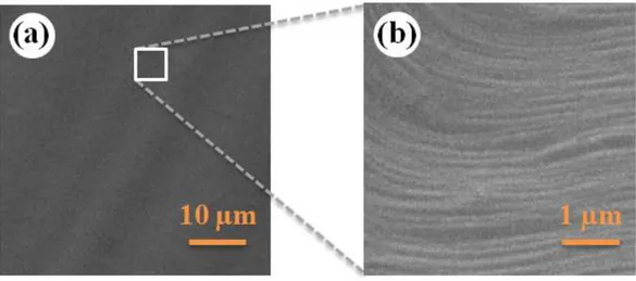
Figure 3.15 A large-scale SEM image which demonstrates overall graphene coverage
on the SiO2/Si substrate ... 39 Figure 3.16 SEM images illustrating common structural defects and contaminants
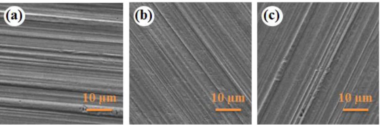
associated with CVD-grown graphene on SiO2/Si substrates such as: (a) White dots
and a torn area, (b) Folded area ... 40
Figure 3.17 Representative SEM images of CVD-grown graphene: (a) G-w/H2, (b)
G-w/oH2, (c) G-UC, and (d) G-AGC ... 40 Figure 3.18 An illustration of a wrinkle on the graphene sample transferred onto the
SiO2/Si substrate ... 41 Figure 3.19 The atomic force microscope used for the experiments presented here
(PSIA XE-100E), available at the National Nanotechnology Research Center (UNAM) ... 42
xiii
Figure 3.20 (a) A topographical AFM image of CVD-grown graphene on SiO2/Si and
(b) its 3D representation. (c) Representative height profile of the boundary between graphene and SiO2/Si. (d) Representative height profile of a wrinkle on graphene .... 43 Figure 3.21 Topographical AFM images of CVD-grown graphene: (a) G-w/H2,
(b) G-w/oH2, (c) G-UC, and (d) G-AGC ... 44 Figure 4.1 A basic sketch of atomic force microscopy, describing the friction force
experienced by the AFM probe during scanning ... 48
Figure 4.2 An illustration of a friction loop arising as a result of lateral forces with
opposite signs recorded in the forward and backward scanning directions ... 49
Figure 4.3 A schematic diagram of the surface structure of TGF11 silicon calibration
grating used for the determination of lateral force calibration factors in this thesis .... 51
Figure 4.4 Representative measurements of the dependence of friction force (Ff) on
normal load (Fn) for CVD-grown graphene, wrinkles, and the SiO2/Si substrate,
together with linear fits to the data ... 53
Figure 4.5 Graph detailing the dependence of friction force (Ff) on normal load (Fn)
for CVD-grown graphene, wrinkles, and the SiO2/Si substrate, for samples of the (a)
G-w/H2 and (b) G-w/oH2 variety ... 55 Figure 4.6 Lateral force maps of CVD-grown graphene on SiO2/Si substrates for
samples with two different growth conditions: (a) G-w/H2 and (b) G-w/oH2 ... 56 Figure 4.7 Graph detailing the dependence of friction force (Ff) on normal load (Fn)
for (a) CVD-grown graphene, (b) wrinkles, and (c) the SiO2/Si substrate, for three
different tips ... 57
Figure 4.8 SEM images of the apex of Tip 3: (a) before, and (b) after AFM
measurements, showing severe degradation ... 58
Figure 4.9 Graph detailing the dependence of friction force (Ff) on normal load (Fn)
for as-transferred and post-transfer-cleaned CVD-grown graphene samples ... 59
Figure 4.10 Graph detailing the dependence of friction force (Ff) on normal load (Fn)
for wrinkles on as-transferred and post-transfer-cleaned CVD-grown graphene samples ... 60
Figure 4.11 Lateral force maps of (a) ultrasonic-cleaned (G-UC), and
(b) Ar-gas-annealed (G-AGC) samples. Dark regions correspond to lower friction forces ... 61
Figure 4.12 Lateral force maps of (a) CVD-grown and (b) mechanically-exfoliated
single-layer graphene samples on SiO2/Si substrate Dark regions correspond to lower
xiv
Figure 4.13 Graph detailing the dependence of friction force (Ff) on normal load (Fn)
for (a) CVD-grown and mechanically-exfoliated graphene samples, and (b) the SiO2/Si substrates on which they are situated ... 63 Figure 4.14 Graph detailing the dependence of friction force (Ff) on normal load (Fn)
for (a) mechanically-exfoliated graphene, and (b) its SiO2/Si substrate, for two
xv
List of Tables
Table 3.1 The comparison of the quality of CVD-grown graphene samples obtained
via different combinations of growth parameters ... 31
Table 4.1 The normal spring constants and lateral force calibration factors of the five
cantilevers used for the nanotribology work presented in this thesis... 51
Table 4.2 The ratios of coefficients of friction of graphene to SiO2 (Graphene/SiO2) .. 67 Table 4.3 The ratios of local friction forces measured on wrinkles to those on
1
Chapter 1
Introduction
1.1 Overview
People who lived in ancient times came up with two outstanding discoveries which were, to a large extent, friction-related. For heating and cooking purposes, they used frictional heating achieved by rubbing two objects in rapid fashion, which is partially responsible for the discovery of fire. Additionally, they discovered that friction forces associated with rolling are generally smaller than those associated with sliding, a discovery that led, at least partially, to the invention of the wheel. From ancient to modern times, friction has had a vital impact in our daily lives: People would not be able to walk, drive, write, or even hold objects without the existence of the friction. On the other hand, excessive friction experienced by surfaces in contact leads to wear and causes dissipation of potentially useful energy via, e.g., generation of heat. On that account, it is desired to reduce friction in many practical applications and devices that feature sliding components, mostly via the use of suitable lubricants. In that context, graphene, a recently discovered two-dimensional material with numerous outstanding physical properties, possesses the potential to be an effective solid lubricant.
This M.S. thesis focuses on the preparation of graphene on copper foils via the method of chemical vapor deposition (CVD), as well as its structural and nanotribological
2
characterization using advanced microscopy techniques. In particular, atomic force
microscopy (AFM) is employed to study the lubrication properties of CVD-grown
graphene transferred onto oxidized silicon substrates (SiO2/Si) as a function of normal
load and post-transfer cleaning procedure. It is projected that the results presented in this thesis will further contribute to a complete physical understanding of frictional properties exhibited by two-dimensional materials and help evaluate graphene’s potential as a solid lubricant in practical applications. In the following sections of this introductory chapter, the significance of friction, nanotribology, and graphene is briefly discussed and finally, an outline of the thesis is provided.
1.1.1 Friction: History and Importance
When an object (usually called the slider) slides on another object (usually called the
substrate), its motion is typically opposed by a friction force. On the other hand, the
force one needs to overcome to make an initially stationary object move on another object is also due to friction. As indicated in the previous section, friction is necessary to prevent slipping and sliding, and thus allows living creatures to be mobile in an efficient fashion. However, it induces energy dissipation which results in significant amounts of economic loss in industrial processes, most prominently in large-scale manufacturing. In various scenarios, friction can be minimized by using lubricants, reducing the weight of the associated objects, or by the use of rolling elements.
Friction has been the subject of a number of documented studies and investigations since hundreds of years. In the site of El-Bersheh, Egypt, a drawing dated 1880 B.C was discovered. This drawing shows a colossus being pulled on a sledge by a group of slaves, and a man (supposedly a mechanical engineer) pouring a liquid lubricant in front of the path of motion of the sledge to reduce frictional resistance to motion (Figure 1.1) [1].
A large number of scientists have worked on the concept of friction throughout history (Figure 1.2). Leonardo da Vinci (1452–1519), who has performed the first
documented scientific studies related to friction and wear, has investigated friction force on horizontal and inclined planes, introduced the concept of the coefficient of
3
unfortunately has not published his work. In year 1979, Duncan Dowson presented Da Vinci’s tribology work (including his notes and sketches on the subject) in his book titled “History of Tribology”. On the other hand, more than hundred years after Da Vinci, Robert Hooke (1635–1703) studied rolling friction and focused specifically on the concept of adhesion [1]. A contemporary scientist with Robert Hooke, Guillaume Amontons (1663-1705), in 1699, rediscovered the first and second laws of friction which were discovered but not published by Da Vinci. Amontons’ first law states that the friction force is directly proportional to the normal load and his second law indicates that the friction force does not depend on the apparent contact area [2]. Leonhard Euler (1707-1783) was the first man who has distinguished static and kinetic friction. Charles-Augustin de Coulomb (1736-1806) has introduced “Coulomb’s Law of Friction” which emphasizes that kinetic friction is independent of the sliding velocity [3]. Additionally, Coulomb has analyzed the influence of the structure of contacting surfaces, the contact area, the normal load between the surfaces, and the elapsed time while the surfaces are in contact, on friction [1]. These observations led to the following common “law of friction”:
μ = 𝐹f/ 𝐹n (1.1)
where µ is the coefficient of the friction (which is a constant that only depends on the type of materials in contact), Ff is the friction force, and Fn is the normal load [4].
Figure 1.1 An Egyptian engineer using a liquid lubricant to aid the movement of a
4
Frank Philip Bowden (1903-1968) and David Tabor (1913- 2005) have later determined that the actual contact area between two objects is significantly less than the apparent contact area as the interface is of multi-asperity character, meaning that it is made up of numerous small regions of contact between the asperities of slider and substrate (Figure 1.2) [5]. This fact introduced a considerable difficulty to the correct physical interpretation of macroscopic friction experiments, as the actual contact area cannot be determined reliably in most practical scenarios. However, the research field of nanotribology, introduced more than two decades ago, has provided an elegant solution to this problem via the utilization of AFM, which will be discussed in the following section.
Figure 1.2 (a) A sketch demonstrating that the apparent contact area at the interface between two macroscopic objects appears reasonably flat. (b) The zoomed-in view of the interface which demonstrates that the actual contact between the two surfaces is of multi-asperity character.
1.1.2 Nanotribology: Searching for the Origins of Friction via Atomic Force Microscopy
Physicist Richard Feynman (1918-1988) is widely regarded as the father of
nanotechnology, due to his well-known lecture titled “There is Plenty of Room at the
Bottom” that he delivered at an APS meeting in CalTech in 1959. Several decades after the lecture by Feynman, nanoscience and nanotechnology have become subjects of intense scientific research and there are already a number of manufacturing methods, devices and other consumer goods on the market that rely on nano-scale components and phenomena. Within this context, it can be argued that the invention of scanning probe microscopy (SPM) methods including scanning tunneling
5
microscopy (STM) [7] and atomic force microscopy (AFM) [8] by Gerd Binnig et al.
(which eventually led to the Nobel Prize in Physics in 1986 [9]) have been the main driving force behind nano-research, due to the capability that they provide in terms of very high (down to atomic-scale) resolution imaging and spectroscopy of surfaces. The Greek word tribos which means “rubbing”, is the origin of the word tribology coined by Peter Jost in 1966 [3]. Tribology is the study of interacting surfaces in relative motion; in other words, it is the “science of friction, wear, and lubrication”. A prefix “nano” is added to the word tribology when the scale of the study descends to the order of nanometers (1-100nm). Over the past few decades, the research field of
nanotribology has become an essential branch of nanoscience and nanotechnology.
As already discussed in the previous section, most surfaces are not perfectly (i.e.,
atomically) smooth on the nanoscale, leading to the so-called multi-asperity character.
While certain characterization methods and tools such as the surface force apparatus (SFA) invented by J. N. Israelachvili and co-workers in the 1970s allow the precise measurement of friction forces acting between specific surfaces in relative motion [10], the invention of the AFM was instrumental in the progress of nanotribology, as the sharp AFM probe tip (curvature of radii typically below 100 nm) presents the opportunity to study friction acting at a single asperity (Figure 1.3) [11].
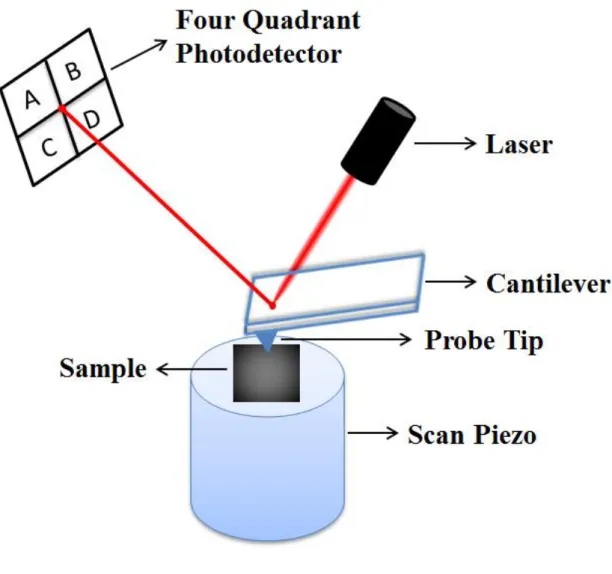
While the details of the AFM method for nanotribology research are discussed in Chapter 4, let us indicate that the basic operating principle relies on the detection of normal and lateral forces experienced by a very soft spring in the form of a micro-machined cantilever via a laser beam deflection (LBD) approach. As already indicated, the cantilever (which is typically fabricated out of Si, SiO2 or Si3N4) is
terminated by a sharp tip apex (the single asperity), which is brought into light contact (normal loads on the order of nN) with the sample surface to be investigated and raster-scanned with pm precision. The interaction of the probe tip with the surface in terms of normal and lateral forces are detected, which allows the study of friction (as inferred from lateral forces) as a function of sample material, normal load, etc., thus contributing remarkably to nanotribology research. For a comprehensive review of significant results achieved by the use of AFM in nanotribology research, the reader is directed to Ref. [12].
6
Figure 1.3 A schematic drawing of the fundamental elements of an AFM, and a
representation of the single-asperity nature of the probe tip on the sample surface. Adapted from www.keysight.com.
1.1.3 Graphene: The “Wonder Material”
The word “graphene”, coined by Hanns-Peter Boehm, originates from the combination of the word graphite and the suffix “–ene” [13]. Graphene is a
two-dimensional material, in the sense that it is essentially a single sheet of carbon
atoms arranged in a honeycomb lattice, which would in principle constitute a single layer of bulk highly oriented pyrolytic graphite (HOPG). Two researchers at the University of Manchester, Andre Geim and Konstantin Novoselov, have accomplished producing, identifying, and characterizing the physical properties of graphene as reported by a series of papers starting in 2004 [14, 15], which eventually
7
led to the awarding of the Nobel Prize in Physics in the year 2010. The prize winning graphene was fabricated by the so-called mechanical exfoliation method, where a bulk HOPG sample is peeled off by ordinary scotch tape, and made repeatedly thinner by folding the tape over itself, with the eventual attachment of single- and few-layer graphene samples to a target substrate (typically SiO2/Si) [14, 15].
Graphene arouses interest both theoretically and experimentally due to its exceptional physical properties [16]. This remarkable material is an allotrope of carbon that consists of sp2-bonded carbon atoms in a two-dimensional honeycomb lattice where the interatomic distance between the carbon atoms is 0.142 nm (Figure 1.4).
Figure 1.4 The structure of graphene.
Among the many interesting properties of graphene, its electrical and mechanical characteristics are of particular importance. Specifically, graphene has a peculiar band structure that results in its behavior as a “zero bandgap two-dimensional semiconductor” where electrons are considered to be massless Dirac fermions [17]. This leads to high electron mobilities of ~10,000 cm2/Vs observed at room temperature for exfoliated graphene samples [15]. On the other hand, pioneering AFM experiments conducted on exfoliated graphene have revealed outstanding mechanical properties associated with this material, namely a Young’s modulus value of ~1.0 TPa and an intrinsic strength of ~130 GPa, at which fracture occurs [18]. The frictional properties of graphene have also been investigated in a relatively small number of
8
publications over the last decade (e.g., Ref. [19, 20]). An overview of related results and how the work presented in this thesis complements the studies in the literature is provided in Chapter 4.
Finally, it should be indicated that in addition to mechanical exfoliation, graphene can be obtained by chemical vapor deposition (CVD) on metal surfaces such as copper [21], as well as epitaxial growth on silicon carbide (SiC) [22]. While each method and the resulting graphene samples have advantages and disadvantages for various applications, the CVD method has been preferred to produce the graphene samples investigated nanotribologically in this thesis, based on the fact that the CVD approach provides single-layer graphene samples on the length scale of centimeters (whereas single-layer graphene flakes produced by mechanical exfoliation are rarely larger than 100 m). As the main aim of the work presented here is to evaluate the lubrication properties of graphene sheets in sizes that would be potentially useful for practical applications, the CVD method has been employed to produce the samples.
1.2 Outline
In this introductory chapter (Chapter 1), the history and importance of friction have been emphasized, and the research field of nanotribology as well as the “wonder material” graphene have been introduced. The chapter underlines that this M.S. thesis is devoted to the nanotribological characterization of CVD-grown graphene via AFM and an evaluation of its potential as a solid lubricant.
In Chapter 2; the preparation, transfer, and post-transfer cleaning procedures associated with CVD-grown graphene are described. The chapter also includes a brief literature review of the CVD process for graphene growth.
Chapter 3 reports the results of the structural and morphological characterization of CVD-grown graphene, as conducted by optical microscopy, Raman spectroscopy, scanning electron microscopy, and atomic force microscopy. The obtained data highlight that single layer graphene sheets of sufficient size are synthesized successfully.
9
Chapter 4 titled “Nanotribological Characterization of CVD-Grown Graphene Transferred onto SiO2/Si Substrates” forms the main part of this M.S. thesis. In this
chapter, the basic operating principle of AFM and the associated force calibration procedures are described first. Subsequently, results of AFM-based nanotribology measurements on CVD-grown graphene are presented. The dependence of friction on normal load is examined in detail. Additionally, the effects of using different tips, employing different growth conditions and performing different post-transfer cleaning procedures on observed friction force values are reported. The chapter includes an overall evaluation of the lubrication performance of CVD-grown graphene on SiO2/Si.
Finally, Chapter 5 provides a general summary of the experimental study presented in the thesis, as well as an outlook regarding future research directions.
10
Chapter 2
Sample Preparation: Chemical Vapor
Deposition, Transfer onto SiO
2
/Si
Substrates, and Post-Transfer Cleaning
2.1 Background
As indicated earlier, the two-dimensional material graphene with its outstanding physical properties has received tremendous attention globally and has recently become one of the so-called hot topics of nano-scale scientific research. One of the main thrusts of graphene research has been placed on gaining the capability to produce single-layer samples on large scales (centimeter-scale and above), while minimizing defect formation. Among various techniques that have been proposed and applied for the production of graphene, the chemical vapor deposition (CVD) method has been so far the most successful in terms of obtaining large-scale graphene samples with single layer character. While the procedural details of the CVD approach to graphene growth are reported in Section 2.2, a brief review of related scientific efforts in the literature is given below.
In the year 2006, Somani et al. wrote the first report related to synthesis of few-layer graphene on nickel substrates via the pyrolysis of camphor, utilizing a CVD-based approach [23]. The first study involving single- to few-layer graphene growth via
11
CVD of methane (CH4) on polycrystalline nickel films, and the subsequent transfer of
the resulting material to arbitrary substrates such as SiO2/Si (i.e., an oxidized Si wafer)
was realized by Reina et al. [24]. Shortly after the mentioned work, the synthesis of high quality and large-scale graphene with uniform single-layer character was achieved by X. Li et al. via the CVD of CH4 on a 25 µm thick copper foil [21].
Following the demonstration of the CVD growth of single- and few-layer graphene on copper and nickel foils, CVD growth of graphene on a 25 µm thick gold substrate has been reported by the group of C. Kocabaş at Bilkent University [25]. The common aspect of the substrates used in the reported studies (Cu, Ni, Au) is chemical in character such that they are all transition metals. In the growth process, the transition metal surfaces act as catalysts for the decomposition of carbon-carrying gases (such as methane) such that carbon atoms are accumulated on the surfaces, eventually forming graphene [26].
After graphene growth via CVD on transition metal surfaces such as copper, it is typically desired to transfer graphene from the metal surface to a target substrate (such as SiO2/Si) for potential use in various applications. However, transfer procedures
associated with graphene are quite challenging, mainly due to the occurrence of structural damage (such as the formation of tears and folds) and potential contamination (due to the chemicals involved in the process) during the transfer. The considerable lateral sizes of graphene sheets grown via CVD also cause practical problems associated with transfer to a new substrate. The transfer procedure associated with CVD-grown graphene typically involves a polymer handle layer such as poly (methyl methacrylate) PMMA [27, 28, 29], poly (dimethylsiloxane) PDMS
[30], thermal release tape [31], self-release layer (SRL) [32], or poly (bisphenol A carbonate) PC [33]. Among these, the PMMA-based transfer
method is the most commonly used, mainly due to its procedural simplicity. PMMA, which is used as a sacrificial handle layer in the transfer process, inevitably leaves a certain amount of chemical residue on the graphene samples after transfer to different substrates. In order to clean the chemical residue on graphene, post-transfer cleaning steps can be employed. There are several cleaning procedures practiced in the literature, as further explained in Section 2.4.
12
This chapter is devoted to the procedural details associated with the preparation of graphene samples (in particular; CVD growth, transfer, and post-transfer cleaning), the nanotribological properties of which are subsequently analyzed via AFM as reported in Chapter 4.
2.2 Graphene Growth on Copper Foils via CVD
2.2.1 Basic Principle of the CVD Process
The chemical vapor deposition (CVD) process is a common bottom-up microfabrication method used for producing thin films (chiefly in the semiconductor industry), involving the deposition and subsequent decomposition of gaseous precursors on a substrate which is typically held at elevated temperatures to facilitate the involved chemical reactions. There are plenty of variations of CVD; foremost among them are atmospheric pressure CVD (APCVD), low pressure CVD (LPCVD), and ultrahigh vacuum CVD (UHVCVD). APCVD operates at atmospheric pressure, LPCVD works at under sub-atmospheric pressures and UHVCVD is functional at extremely low pressures (~10-8 mbar or lower) [34].
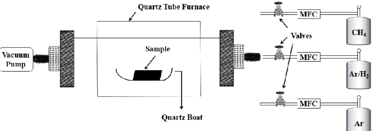
Figure 2.1 A schematic diagram of a typical CVD system based on a quartz tube
furnace.
A typical CVD system is composed of a furnace that acts as the reaction chamber and the source of thermal energy as well as the manifold system for the delivery of the
precursor/carrier gases to the reaction chamber, a vacuum pump for the removal of by-products in the form of unwanted gases, and process control equipment such as
13
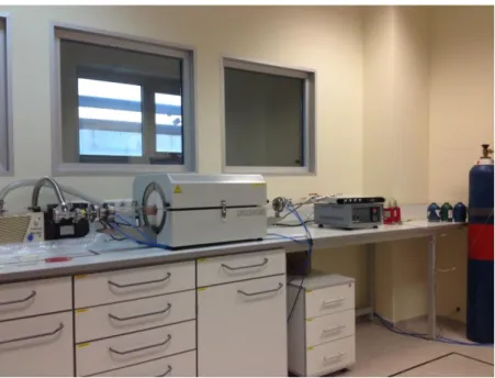
mass flow controllers (MFCs) and valves (Figure 2.1). A picture of the CVD system used for the experiments reported in this M.S. thesis is provided in Figure 2.2.
Figure 2.2 A picture of the CVD system at the National Nanotechnology Research
Center (UNAM) used for the experiments reported in thesis.
The sequence of the steps in a typical CVD process starts with the transport of the precursor gases to the heated reaction chamber and adsorption of these gases on the substrate surface. The process continues with the surface diffusion of precursor gases to the growth sites, chemical reactions leading to decomposition and eventual deposition of the resulting material on the substrate surface, accompanied by the desorption of gaseous by-products. As already indicated, the disposal of the gaseous by-products from the reaction chamber is usually performed by a vacuum pump. At the end of the process, the substrate is coated with a thin film of the desired material. It should be noted that the chemical reaction to break the bonds within the precursor gases is provided by the heat from the resistive elements in the furnace. The sample surface acts as a catalyst, reducing the energy barriers required for decomposition. The gases that are used in the process must be volatile and stable so as to be able to reach the reaction chamber and react with the substrate. As already indicated, the CVD approach is the preferred method for graphene production in this M.S. thesis, mainly due to the large size of the resulting samples.
14
2.2.2 Graphene Growth via CVD: Choice of Substrate
As a first step in the CVD process, the selection of the transition metal which is to be used as the substrate must be performed. In the literature, copper and nickel foils are widely used as catalysts for the CVD process. Due to significant differences in the solubility of carbon in the two materials, the growth mechanism differentiates for copper and nickel substrates. The solubility of carbon in copper is two orders of magnitude smaller than nickel (0.001% vs. 0.1%). This leads to the fact that CVD-growth on copper performed via methane at elevated temperatures (near 1000 oC) results in almost uniform coverage of the substrate by single-layer graphene, while graphene grown on nickel features a large amount of multi-layer regions, caused by the precipitation of excess carbon in bulk Ni upon cooling of the foils due to the associated decrease in carbon solubility [35].
As a substrate for the growth of single-layer graphene samples, 25 µm thick copper foil with 99.8% purity (Alfa Aesar, product no. 13382) has been chosen, in accordance with reports in the literature [21]. The foil is cut in dimensions of 35 mm 50 mm to be placed in quartz boats acting as carriers in the quartz tube furnace used for graphene synthesis.
It has been observed that the surface morphology and cleanliness of the copper foil significantly affect the quality of CVD-grown graphene. As such, a cleaning process is performed on the copper foils, with the intention of improving graphene quality by reducing surface roughness and removing organic impurities on the surface of the copper foil. The cleaning procedure begins by dipping the copper foils in acetone to remove organic impurities on the surface. However, as the evaporation rate of the acetone is very high, it leaves certain residues on the surface, which are removed in the second step of the cleaning procedure by isopropanol. In the next step, a diluted acid solution is prepared with 10 ml HCl and 90 ml double-distilled water. The copper foil is sunk into this solution for 5 minutes. Immersion into a double-distilled water bath follows the previous step to remove acid residues. Finally, the foil is dried with a nitrogen gun.
15
Figure 2.3 SEM images of the (a) as-received copper foil; (b) copper foil cleaned with
diluted HCl acid solution, and (c) copper foil cleaned with diluted acetic acid solution. To compare the effectiveness of the HCl acid in the context of foil preparation with another strong acid, acetic acid has been utilized. In Figure 2.3, SEM images of as-received copper foils, as well as those treated with HCl and acetic acid can be seen. In terms of surface morphology, it is observed that the as-received copper foil features the roughest texture, while the foil cleaned with HCl has the smoothest surface. Accordingly, the use of HCl acid solution in the treatment of Cu foils has been preferred in CVD experiments.
2.2.3 Graphene Growth via CVD: Experimental Procedure
For the experiments reported in this thesis, CVD growth has been performed using the system depicted in Figure 2.2, consisting of a quartz tube furnace (Protherm/AlserTeknik), a digital temperature controller (Honeywell DC1020), a vacuum pump (Varian DS202), and mass flow controllers (HoribaStec SECE40). The gas manifold attached to the gas cylinders and including various valves has been built using 316L stainless steel pipes. As oxygen leakage from the air causes oxidation of the copper foil at elevated temperatures and thus inhibits CVD growth, potential gas leaks have been regularly checked via helium leakage tests conducted with a standard instrument (Pfeiffer Vacuum Smart Test HLT570).
The first step in the CVD processes involves placing the copper foil prepared as in Section 2.2.2 into a quartz boat which is then loaded into the quartz tube furnace. The copper foil in its initial form typically features a thin oxide layer on top of its surface despite the cleaning steps discussed previously. The existence of this oxide layer is
16
detrimental for graphene growth as it leads to a reduction in catalytic activity. Therefore thermal annealing is applied on the copper foil in the presence of a reductive element such as hydrogen to get rid of the oxide layer. This process involves heating the furnace to 1000°C, and flowing of a mixture of H2 and Ar gases (ratio
5:95) at 200 sccm (standard cubic centimeters per minute) for 30 minutes over the Cu foil. The thermal annealing process also increases the average grain size on the copper foil surface and thus reduces the negative effect of grain boundaries on the morphology of CVD-grown graphene [36]. SEM images of thermally annealed copper foils are provided in Figure 2.4 for reference.
Figure 2.4 (a) SEM image of thermally-annealed copper foil. (b) Zoomed-in view of
the marked portion, showing terraces separated by steps.
After thermally annealing the Cu foil, graphene growth is initiated with the introduction of CH4 into the quartz tube, typically at 25 sccm. As already discussed,
CH4 is the source of carbon atoms which act as the building blocks of graphene on
copper. The gas valves are closed and the furnace heating system is turned off after 20 minutes of CH4 flow. The cover of the furnace is opened to increase cool-down rates.
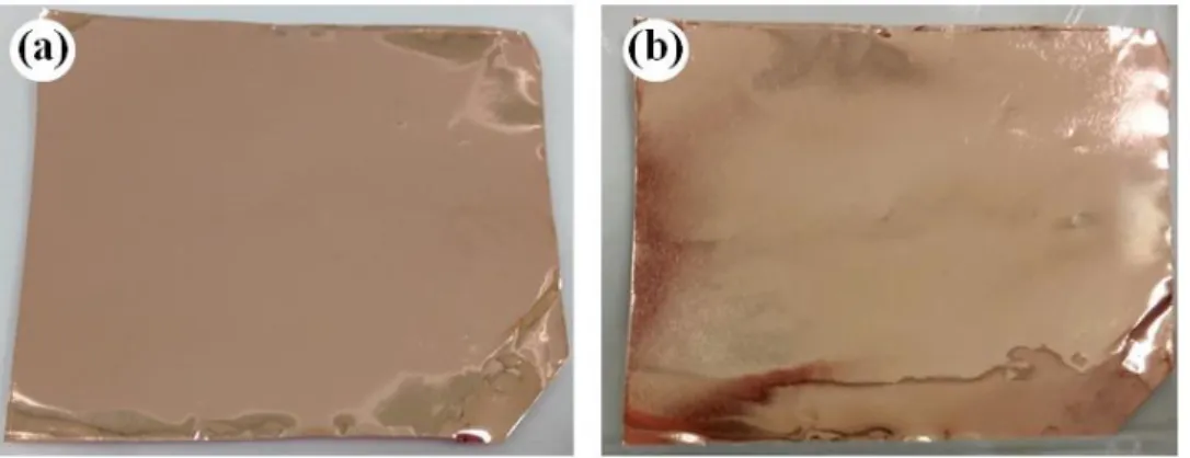
When room temperature is reached in the furnace, the vacuum pump is turned off and the sample is taken out of the quartz tube. The clearly observable difference in the appearance of the copper foils before and after the CVD process due to coverage by graphene is depicted in Figure 2.5.
17
Figure 2.5 Copper foils (a) before, and (b) after graphene growth.
To obtain high quality graphene via CVD, it is important to optimize growth parameters, including temperature, flow rate and flow time of precursor and carrier gases. Due to the large number of involved parameters, lots of variations need to be tested to arrive at optimum conditions. For instance, two different approaches involving either (i) the simultaneous flow Ar/H2 mixture and CH4 or (ii) the flow of
CH4 only during graphene growth can be applied. A comparison of the quality of
graphene grown via different combinations of experimental parameters is provided in Chapter 3.
2.3 Transfer of CVD-Grown Graphene onto SiO
2/Si
Substrates
Once graphene is grown via CVD, it is typically desired to transfer it from the copper foil to an insulating surface for, e.g., electronic applications. Silicon wafers covered with silicon dioxide (SiO2/Si) are traditionally preferred towards this purpose, as it has
been shown that single- and few-layer graphene is optically observable on Si wafers covered with ~300 nm SiO2 using a regular microscope [14].
In order to obtain clean graphene samples on SiO2/Si samples, the level of
contamination in the environment must be very low during the transfer. As such, the whole transfer procedure has been performed in the cleanroom facility of the National Nanotechnology Research Center (UNAM) for the experiments reported here. The
18
high-efficiency particulate air (HEPA) filters [37], providing optimum conditions for graphene transfer.
A sacrificial layer of poly (methyl methacrylate) (PMMA) with the chemical formula of (C5O2H8)n has been used to support (i.e., hold) the CVD-grown graphene during the
transfer process. As the first step of the transfer procedure, the copper foil covered with graphene is put onto a spin-coater and 5 droplets of PMMA 950 A2 are dropped onto it. The duration of spinning and the number of revolutions per minute are adjusted as 50 seconds and 4000 rpm, respectively. After the spin coating procedure, the sample is cured on a 110°C hot plate for 15 seconds. The sample is then cut according to the dimensions of the SiO2 wafer (10 mm 10mm), and is straightened
with the aid of clean, flat handles of a pair of tweezers.
Next, a diluted nitric acid (HNO3) solution is prepared by 5 ml nitric acid and 15 ml
distilled water. In the quartz tube furnace, graphene coats both sides of the copper. First, graphene on the side of the foil not covered by PMMA must be etched away via HNO3 in order to etch the copper beneath it. The HNO3 solution etches the graphene
in ~3 minutes and etching becomes apparent by the rising of plenty of bubbles to the surface of the solution. It is important in this step to make sure that the top surface of the foil (covered with PMMA) does not come into contact the solution. After the graphene etching process, the sample is dipped into distilled water to get rid of the residues associated with the HNO3 solution.
To etch the copper foil away, a 1 M solution of ammonium persulfate [(NH4)2S2O8] is
prepared and put on a hot plate at 70 oC [38]. Consequently, the copper foil is placed on the solution. The duration of the copper etching process is approximately 20 minutes. The colorless solution gradually becomes blue as the copper is etched away. What remains behind is CVD-grown graphene, coated by PMMA.
Subsequently, SiO2/Si wafers are cleaned ultrasonically in baths of acetone,
isopropanol and distilled water. One wafer piece with relatively large dimensions is used as a handling tool and another one is used as the substrate. The larger SiO2 wafer
is utilized to fish the PMMA-covered graphene sample from the copper etchant solution and to place it in a beaker of distilled water in order to remove chemical residues associated with the etching process. Afterwards, the PMMA-covered
19
graphene sample is placed on the substrate SiO2/Si wafer directly from the distilled
water. Attention must be paid in this step to avoid excessive structural damage to graphene. Finally, to remove the PMMA support on graphene, the wafer is placed into acetone for 5 minutes. The whole transfer procedure is visualized in Figure 2.6.
Figure 2.6 The process flow associated with the transfer of CVD-grown graphene
onto silicon oxide substrates. Please note that the relative thickness of the layers is not in scale.
2.4 Post-Transfer Cleaning
As indicated in the previous section, PMMA serves as a supporting layer for graphene in the transfer process. Placing the PMMA-graphene stack in acetone is often not sufficient to remove the whole PMMA layer from graphene – residues are commonly observed, even with optical microscopy. Instead of using acetone as a solvent, dipping the sample into glacial acetic acid for 24 hours and then cleaning it in a methanol solution has been proposed as a way of dissolving PMMA better than acetone [39]. On the other hand, thermal annealing procedures have been also suggested to obtain clean graphene samples with minimal PMMA residues. In the literature, a wide range of thermal annealing procedures have been studied. Graphene samples contaminated
20
by chemical residues have been annealed in vacuum [40] as well as in the presence of Ar [27], Ar/H2 [41], CO2 [42], and N2 [43] gases. Even under harsh conditions
involving high temperatures and extended annealing times, the residuals of PMMA are never entirely removed from the graphene surface [44].
One of the aims of this thesis is to investigate the effect of different post-transfer cleaning procedures (see the two sections below) involving ultrasonic cleaning in acetone and isopropanol, as well as annealing under Ar gas, on the structural and nanotribological properties of graphene. The related results are presented in Chapter 3 and Chapter 4, respectively.
2.4.1 Ultrasonic Cleaning
Ultrasonic cleaning in various solvents is known to be effective in removing contaminants from various sample surfaces. The main working principle of the process is based on agitation of the cleaning medium (the solvent) via ultrasonic excitation to form cavitation bubbles on the surface of the object to be cleaned. Ultrasonic cleaning takes place in a tank containing the solvent, to which an ultrasonic transducer is attached. In this thesis, we evaluated the effect of post-transfer ultrasonic cleaning on the structural and nanotribological properties of CVD-grown graphene. Accordingly, the SiO2/Si wafer covered with graphene is placed into a beaker
containing acetone, which is then inserted in the tank of the cleaner. Next, the sample is cleaned in the ultrasonic cleaner for 20 seconds. Subsequently, the same treatment is applied to the sample in isopropanol. Finally, the sample is dried with nitrogen gas.
2.4.2 Annealing under Argon Flow
Motivated by attempts at removing PMMA residues via annealing under vacuum and Ar gas as reported in the literature [27, 40], we have evaluated the effect of thermal annealing under Ar flow on the structural and nanotribological properties of CVD-grown graphene. Towards this purpose, the SiO2/Si wafer covered with
graphene has been annealed in the quartz tube furnace, post-transfer, under Ar gas flow at 300°C for 2 hours.
21
Chapter 3
Structural and Morphological
Characterization of CVD-Grown
Graphene
3.1 Background
In Chapter 2, the procedural details associated with the growth, transfer, and optional post-transfer cleaning of graphene obtained by the CVD method have been described. On the other hand, before a comprehensive nanotribological characterization of CVD-grown graphene transferred onto SiO2/Si substrates can be accomplished, the
structural and morphological properties of the material in question should be investigated in detail.
Since the demonstration that graphene can be readily obtained by mechanical exfoliation about a decade ago, a diverse range of characterization tools including optical microscopy [14], Raman spectroscopy [45], scanning electron microscopy (SEM) [21], and atomic force microscopy (AFM) [46] have been employed to characterize the structural and morphological properties of graphene samples obtained via various means. In particular, such studies targeted a precise determination of the number of layers of graphene, its distribution and coverage on various substrates, as
22
well as a characterization of associated structural defects including but not limited to wrinkles, tears, and folds.
In this chapter, in line with the available literature on the subject, results of structural and morphological characterization studies on CVD-grown graphene films performed via optical microscopy, Raman spectroscopy, SEM, and AFM are presented; preceded by a brief overview of each method. The data discussed here demonstrates that single-layer graphene samples are successfully obtained via the approach presented in Chapter 2, and a detailed characterization of associated defects and contaminants is possible by employing the experimental techniques mentioned above.
3.1.1 Optical Microscopy and Graphene
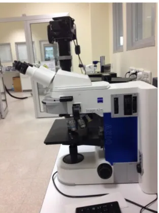
When investigating the physical properties of any material, the first step involves macroscopic observation by naked eye, such that a rough idea about the structural and optical properties of the material is obtained. Obviously, the human eye is a limited observation tool for detailed scientific studies, due to its inability to discern micro-scale structural features. However, as it has been known for centuries, the sense of sight can be extended by optical instruments. In modern science, to study microscopic structural properties, an optical microscope can be used. A typical optical microscope illuminates the sample in question with visible light, and utilizes a system of lenses to obtain a magnified two dimensional image (Figure 3.1).
In the late 16th century Zacharias Jansen (1580-1638) invented a compound optical microscope with two lenses. The objective lens displays a primary, magnified image, and the second lens called the eyepiece is utilized for further magnification of the primary image [47]. Robert Hooke (1635-1703) improved the instrument by adding useful components such as a stage for holding the studied sample, coarse and fine focus control units for lateral and vertical positioning during imaging, and a dedicated illuminator. Perhaps more importantly, Carl Zeiss (1816-1888) and Ernst Abbe (1840-1905) enhanced the resolution of the optical microscope by (i) utilizing a condenser lens which concentrates light from the light source onto the sample and (ii) using lenses with superior optical quality (which mainly involves reduced surface roughness) [48].
23
Figure 3.1 A schematic diagram of a typical, compound optical microscope.
Figure 3.2 An optical microscopy image of mechanically-exfoliated graphene [14].
In one of their landmark papers describing the physical properties of mechanically exfoliated graphene, Novoselov et al. demonstrated that single-layer graphene, which is transparent to visible light, can be detected via optical microscopy (due to the increase in the optical path of visible light induced by the presence of the graphene) when placed on an oxidized Si wafer (SiO2/Si) where the thickness of the oxide is
~300 nm [14]. In Figure 3.2, a representative optical microscope image of a mechanically-exfoliated graphene sample can be seen.
24 3.1.2 Raman Spectroscopy and Graphene
Raman spectroscopy is a widely-employed method which is used towards the chemical identification of various materials. The basic operating principle of Raman spectroscopy is based on the following: Monochromatic light from a laser source is used to illuminate the sample under investigation. As the laser light interacts with the sample, most of the photons are elastically scattered with no loss of energy, which constitutes Rayleigh scattering. However, a smaller amount of incident photons are inelastically scattered (due to interactions with the phonons of the sample), such that their energy either increases or decreases upon interacting with the sample, which is referred to as Raman scattering. By detecting the energy shift associated with scattered photons, which is unique for different materials, detailed chemical identification can be performed [49].
Figure 3.3 The basic functional components of a Raman microscope.
A typical Raman spectroscopy system has three main components, which are: (i) a monochromatic laser used as the excitation source, (ii) a notch filter, and (iii) a spectrometer with a charge coupled device (CCD) detector. The notch filter blocks scattered light with the exact wavelength of the excitation laser such that only energy-shifted (inelastically scattered) photons enter the spectrometer. The spectrometer with the CCD detector is used to detect the intensities associated with a
25
narrow region of wavelengths around the wavelength of the excitation laser (Figure 3.3).
The Raman effect described above has been discovered in year 1928 by Sir Chandrasekhara Venkata Raman (1888-1970). Consequently, in 1930, he was awarded with the Nobel Prize in Physics [50]. Interestingly, he actually utilized sunlight as an excitation source for his pioneering experiments, since the first laser was developed by Theodore Harold Maiman (1927-2007) only in 1960 [51].
Figure 3.4 Comparative Raman spectra of graphite and mechanically-exfoliated,
single-layer graphene, obtained with a monochromatic (514 nm) laser source [45]. Shortly after the demonstration that graphene can be readily obtained by mechanical exfoliation of graphite by Novoselov et al. [14], Raman spectroscopy has been employed to characterize its structure and chemistry by Ferrari et al. [45]. Specifically it has been shown that the number of layers of graphene samples can be precisely determined by such an approach [45]. The Raman spectrum of graphene features three main peaks which are referred to as the D, G, and 2D peaks. The positions of the D, G, and 2D peaks are approximately 1350 cm-1, 1580 cm-1, and 2700 cm-1, respectively [45]. The D peak appears due to structural defects associated with graphene, such that in an ideal graphene sample the D peak should not be detectable. It has been shown by
26
Ferrari et al. that the relative intensities of the 2D peak and G peak (I2D/IG, or simply
I2D/G) can be utilized in the differentiation of single-layer, bi-layer, and multi-layer
graphene samples, such that I2D/G ratios of 2, ~1, and <1, are typically expected for
each case, respectively. Figure 3.4 shows the classic Raman spectra obtained by Ferrari et al. on bulk graphite, as well as a single-layer, mechanically-exfoliated graphene sample. Note that, in addition to the I2D/G ratio, variations in the shape of the
2D peak as well as its Raman shift value may be used as identifiers to distinguish single-layer graphene samples from bi-layer and multi-layer (i.e., graphite-like) specimens.
3.1.3 Scanning Electron Microscopy and Graphene
As mentioned previously, optical microscopy is useful as a first step in materials characterization as it readily produces magnified two-dimensional images of a large variety of sample systems. On the other hand, the resolution achievable by optical microscopy is fundamentally limited by the wavelength of visible light. As such, in modern materials science studies, the scanning electron microscope (SEM) is typically employed to perform high-resolution (conventionally down to ~10 nm) structural characterization of sample surfaces. The increased spatial resolution achieved by SEM when compared to optical microscopy is based on the fact that it uses a high-energy (measured in kV) beam of electrons for imaging rather than visible light.
The basic operating principle of the SEM can be summarized as follows: An electron gun (e-gun) generates thermionically emitted electrons which are accelerated to high energies by a positively charged anode plate. The high-energy electrons passing through the anode are focused via electromagnetic lenses towards the sample surface to be investigated. Scanning coils are used to generate magnetic fields such that the electron beam is scanned over the sample surface in the lateral x and y directions. The electrons that reach the sample surface are called primary electrons. Primary electrons scatter from the sample surface and also promote the ejection of electrons from the atoms of the sample surface. Incident electrons bouncing from the sample surface with high energies as a consequence of elastic scattering are termed backscattered
electrons which typically provide information about the chemical identity of the
27
surface. On the other hand, low-energy electrons that are emitted from the atoms of the sample surface due to inelastic scattering are called secondary electrons and are utilized to detect surface topography as their number depends on the angle formed by the incident electron beam and the structural features of the sample surface. Detectors dedicated to backscattered and secondary electrons coupled to a screen consequently convert the signals from incident electrons to optical images of the surface, sensitive to surface chemistry and topography, respectively (Figure 3.5) [52].
Figure 3.5 A simplified diagram of a scanning electron microscope (SEM).
Ernst Ruska (1906-1988) is the main person who is credited with the first design of an electron microscope, which eventually led to the awarding of the Nobel Prize in Physics in 1986. The very first version of a functional SEM was built by German Scientist Max Knoll in 1935 [53].
In the literature, SEM has been intensely used to investigate the structural and morphological features of graphene obtained via different means. In particular, SEM
![Figure 1.1 An Egyptian engineer using a liquid lubricant to aid the movement of a sledge carrying a large statue, in El-Bersheh, Egypt, in 1880 B.C [6]](https://thumb-eu.123doks.com/thumbv2/9libnet/5897897.121996/18.892.177.792.710.1033/figure-egyptian-engineer-liquid-lubricant-movement-carrying-bersheh.webp)
![Figure 3.4 Comparative Raman spectra of graphite and mechanically-exfoliated, single-layer graphene, obtained with a monochromatic (514 nm) laser source [45]](https://thumb-eu.123doks.com/thumbv2/9libnet/5897897.121996/40.892.247.720.349.728/figure-comparative-graphite-mechanically-exfoliated-graphene-obtained-monochromatic.webp)