SEMICONDUCTOR QUANTUM DOTS DRIVEN BY
RADIATIVE AND NONRADIATIVE ENERGY
TRANSFER FOR HIGH-EFFICIENCY HYBRID LEDs
AND PHOTOVOLTAICS
A THESIS
SUBMITTED TO THE DEPARTMENT OF ELECTRICAL AND ELECTRONICS ENGINEERING
AND THE GRADUATE SCHOOL OF ENGINEERING AND SCIENCE OF BILKENT UNIVERSITY
IN PARTIAL FULLFILMENT OF THE REQUIREMENTS FOR THE DEGREE OF
MASTER OF SCIENCE
By
Burak Güzeltürk
August 2011
ii
I certify that I have read this thesis and that in my opinion it is fully adequate, in scope and in quality, as a thesis for the degree of Master of Science.
Assoc. Prof. Dr. Hilmi Volkan Demir (Supervisor)
I certify that I have read this thesis and that in my opinion it is fully adequate, in scope and in quality, as a thesis for the degree of Master of Science.
Assoc. Prof. Dr. Vakur B. Ertürk
I certify that I have read this thesis and that in my opinion it is fully adequate, in scope and in quality, as a thesis for the degree of Master of Science.
Prof. Dr. Engin Umut Akkaya
Approved for the Graduate School of Engineering and Science:
Prof. Dr. Levent Onural
iii
ABSTRACT
SEMICONDUCTOR QUANTUM DOTS DRIVEN BY
RADIATIVE AND NONRADIATIVE ENERGY
TRANSFER FOR HIGH-EFFICIENCY HYBRID LEDs
AND PHOTOVOLTAICS
Burak Güzeltürk
M.S. in Electrical and Electronics Engineering
Supervisor: Assoc. Prof. Dr. Hilmi Volkan Demir
August 2011
Today the world energy demand has overtaken unprecedented consumption levels, which have never been reached before in the history of the world. The current trends indicate that the increasing demand for energy will tend to continue at an increasing pace in the coming decades due to worldwide globalization and industrialization. Scientific community is challenged to devise and develop fundamentally new technologies to cope with the energy problem of the world. To this end, optoelectronics can offer several solutions for energy efficiency both in light harvesting and generation. In this thesis, we propose and demonstrate enhanced light generation and harvesting by utilizing both radiative and nonradiative energy transfer capabilities of semiconductor nanocrystal quantum dots, which are profited for the development of novel hybrid devices combining superior properties of the constituent material systems. One of our proposals in this thesis relies on grafting nanostructured light emitting diodes with nanocrystal quantum dots to realize highly efficient color conversion. To the best of our knowledge, we report the highest nonradiative energy transfer efficiency of 83% obtained at room temperature for this type of color-conversion light emitting diodes owing to the architectural superiorities of their nanostructure. In another proposal, we addressed charge injection problems of electrically pumped nanocrystal-based light emitting diodes. We proposed and demonstrated the utilization of novel excitonic injection scheme to drive such LEDs of nanocrystals, which may become prominent especially for the display
iv
technology. Finally, we proposed and implemented quantum dot down-conversion layers in nanostructured silicon solar cells to benefit the advantages of their nanostructured architecture. We have shown that nanostructured silicon solar cells lead to stronger enhancements compared to the planar counterparts. Keywords: Nanocrystals, quantum dots, light emitting diodes (LEDs), solar cells, nonradiative energy transfer, excitonics.
v
ÖZET
YARI ILETKEN NANOKRĠSTAL KUVANTUM
NOKTACIKLARIN IġIMALI VE IġIMASIZ ENERJĠ
TRANSFERĠ KULLANIMI ĠLE VERĠMLĠLĠĞĠ
ARTIRILMIġ MELEZ IġIK YAYAN DĠYOTLAR VE
GÜNEġ GÖZELERĠ
Burak Güzeltürk
Elektrik ve Elektronik Mühendisliği Bölümü Yüksek Lisans Tez Yöneticisi: Doç. Dr. Hilmi Volkan Demir
Ağustos 2011
Günümüzde dünyanın enerji ihtiyacı Ģimdiye kadar hiç ulaĢılmamıĢ tüketim seviyelerine çıkmıĢ bulunmaktadır. Yapılan tahminlere göre dünyadaki hızlı büyüme ve globalleĢme enerji tüketimini gelecekte daha da artıracaktır. Bilim dünyası daha verimli enerji üretim ve kullanım teknolojileri geliĢtirebilmek için yoğun bir uğraĢ vermektedir. IĢık ve elektronik teknolojilerini birleĢtiren optoeletronik dalı, güneĢ gözeleri ve ıĢık yayan diyotlar ile enerji üretim ve kullanım problemine verimli çözümler sunmaktadır. Bu tezde, yarı iletken nanokristal kuvantum noktacıklarının ıĢımalı ve ıĢımasız enerji transferi özelliklerini kullanarak, güneĢ pillerinin ve ıĢık yayan diyotların verimliliklerini artırmaya yönelik çalıĢmalar önerdik ve uygulamalarını gösterdik. Nano-sütun mimarisine sahip mavi ıĢıyan diyotları daha uzun dalga boyunda ıĢıyan nanokristaller ile melezleĢtirerek, nano-sütun yapısının sağladığı üstün mimari özellikleri sayesinde, diyotların yapı taĢı kuvantum kuyular ile kuvantum noktacıkları arasında Ģimdiye kadar bilgimiz dahilinde rapor edilmiĢ en yüksek % 83‟lük enerji transfer verimliliğini elde ettik. Bu sayede, renk dönüĢtürücülü ıĢık yayan diyotlar için gelecek vaadeden melez tasarımlar önerdik. Bundan baĢka, yük pompalaması metodu ile çalıĢan nanokristal tabanlı ıĢık yayan diyotlarda yaĢanan yük sürme problemine çözüm olarak özgün ve yeni bir metot geliĢtirdik. IĢımasız enerji transferi sayesinde uyarım enerjisini doğrudan nanokristallere pompalayarak elektro-ıĢıma yapapabilen nanokristal tabanlı ıĢık
vi
yayan diyotları geliĢtirdik. Son olarak, silisyum tabanlı güneĢ pillerinin temel sorunlarından biri olan kısa dalga boyundaki ıĢığın verimsiz dönüĢtürülmesi problemine çözüm olarak nano-sütun yapısında olan silisyum güneĢ gözelerinin ıĢığı yüksek dalga boyuna çeviren nanokristaller ile birleĢtirilmesini gösterdik. Nano-sütun yapısı sayesinde, ıĢığın sütunlar arasına hapsedilmesinden dolayı, klasik düz mimarilere göre kısa dalga boyunda çok daha fazla iyileĢtirme sağladık.
Anahtrar Kelimeler: Nanokristaller, kuvantum noktacıkları, güneĢ pili, ıĢık yayan diyot, ıĢımalı ve ıĢıması enerji transferi.
vii
Acknowledgements
On the verge of finishing my Master‟s degree, I feel happy that I have made the right decision of pursuing an academic career in interdisciplinary branches of science. Three years ago, I have joined the group of Prof. Hilmi Volkan Demir when I was just starting my senior year. Through these years, I have learned a lot from him both technically and personally. I would like to thank him for his contributions and guidance.
This thesis would not be possible without our good friends and colleagues. First, I would like to thank all past and present Demir group members for being always helpful and friendly to me. Specially, I would like to thank Evren Mutlugün and Dr. Sedat Nizamoğlu from whom I have learned my basic lab skills and they always responded whenever I asked for help. I would like to thank Tuncay Özel, Özge Özel, Emre Ünal, Dr. Rohat Melik, Emre Sarı and Can Uran, my seniors in the group, who always helped me and guided me very well. I would like to thank Dr. Nihan KoĢku Perkgöz, Özgün Akyüz, Dr. Olga Samarskaya, Dr. Urartu Ö. ġ. ġeker, Gülis Zengin, Neslihan Çiçek, Mustafa Akın Sefunç, Onur Akın, Gürkan Polat, Aslı Ünlügedik, Talha Erdem, Veli Tayfun Kılıç, Hatice Ertuğrul, Sina Toru, Sayım Gökyar, Uğur Karatay, Cüneyt Eroğlu and Kıvanç Güngör, Dr. Ludwig P. Hernandez-Martinez, Shahab Akhavan, Yusuf KeleĢtemur, A. Fatih Cihan, Ozan Yerli, Yasemin CoĢkun, Aydan Yeltik, Togay Amirahmadov, Dr. Vijay Kumar Sharma and Onur Erdem for always being kind, helpful and friendly.
I would like to thank engineers and laboratory staff in UNAM and ARL who made our lives easier all the time.
I would like to acknowledge and thank TUBĠTAK-BĠDEB (2210 - Yurt Ġçi Yüksek Lisans Burs Programı) for the financial support throughout this thesis.
viii
I would like thank Nisa YeĢilgül without whom these last two years will be less colorful.
Finally, I would like thank my parents Halit and Nesrin for being always there whenever I need them along with their enormous patience and love.
ix
Table of Contents
1. INTRODUCTION ... 1
1.1MOTIVATION OF THE THESIS... 1
1.2ORGANIZATION OF THE THESIS ... 4
2. SCIENTIFIC BACKGROUND ... 6
2.1PHOTOVOLTAIC SOLAR CELLS ... 6
2.1.1 Principles of Operation ... 6
2.1.2 Important Device Parameters and Characterization Techniques ... 10
2.2SEMICONDUCTOR LIGHT EMITTING DIODES ... 15
2.2.1 Principles of Operation ... 15
2.2.2 Organic Light Emitting Diodes... 18
2.2.3 Important Parameters and Characterization... 23
2.3EXPERIMENTAL METHODS... 26
2.3.1 Fluorescence Lifetime Spectroscopy ... 26
2.3.2 Steady State Optical Characterizations... 27
2.3.3 Material and Structural Characterizations ... 29
2.3.4 Fabrication Techniques ... 30
3. SEMICONDUCTOR QUANTUM DOT NANOCRYSTALS ... 31
3.1INTRODUCTION ... 31
3.2QUANTUM MECHANICS BEHIND NANOCRYSTAL QUANTUM DOTS ... 35
3.3SYNTHESIS OF NANOCRYSTAL QUANTUM DOTS ... 38
3.4PROPERTIES OF NANOCRYSTAL QUANTUM DOTS... 42
3.5APPLICATIONS ... 46
4. RADIATIVE AND NONRADIATIVE ENERGY TRANSFER MECHANISMS . 49 4.1INTRODUCTION ... 49
4.2NONRADIATIVE ENERGY TRANSFER ... 49
4.3RADIATIVE ENERGY TRANSFER ... 57
4.4APPLICATIONS ... 57
5. RADIATIVE ENERGY TRANSFER FROM QUANTUM DOTS TO SILICON NANOPILLARS FOR ENHANCED NOVEL SILICON SOLAR CELLS ... 59
5.1INTRODUCTION AND MOTIVATION ... 59
5.2PROPOSAL AND PRINCIPLES OF OPERATION ... 62
5.3EXPERIMENTS AND RESULTS ... 65
5.4CONCLUSIONS ... 75
6. NONRADIATIVE ENERGY TRANSFER FROM INGAN/GAN MULTI QUANTUM WELL NANOPILLARS TO QUANTUM DOTS: EFFICIENT COLOR CONVERTERS FOR LIGHT EMITTING DIODES ... 76
6.1INTRODUCTION AND MOTIVATION ... 76
6.2PROPOSAL AND PRINCIPLES OF OPERATION ... 80
6.3EXPERIMENTS AND RESULTS ... 82
x
7. SPECIFICALLY ANCHORED POLYMER - QUANTUM DOT HYBRIDS: TEMPERATURE DEPENDENT NONRADIATIVE ENERGY TRANSFER DYNAMICS FOR EXCITONICALLY PUMPED QUANTUM DOT BASED
LIGHT EMITTING DIODES ... 98
7.1INTRODUCTION AND MOTIVATION ... 98
7.2PROPOSAL AND PRINCIPLES OF OPERATION ... 100
7.3TEMPERATURE DEPENDENT NONRADIATIVE ENERGY TRANSFER DYNAMICS ... 103
7.4EXCITONICALLY DRIVEN QD-LEDS ... 133
7.5CONCLUSIONS ... 143
8. CONCLUSIONS ... 145
6.1CONTRIBUTIONS ... 147
xi
List of Figures
Figure 2.1.1.1 Schematic representation of a p-n junction diode. Material is excited with photons in the visible range. Photogenerated electron-hole pairs are represented. Due to doping of the material resulting immobile ionized acceptors and donors along with free electrons and holes are shown. Energy vs. position schematic shows the alignment of the p- and n-doped regions with depletion region where built-in electric field exists. ... 8 Figure 2.1.1.2 Principle of operation of a solar cell is depicted. Electron and hole
pair is created via photo-generation. A minority carrier (e.g., a hole in this case) diffuses in the region (1, 2). If it can reach the junction (i.e., depletion region) after diffusing (3), it is drifted to the other region where it is
majority carrier (4). Due to this drift current, in the external circuit, the majority carrier (e.g., electron in this case) is given to external circuit (5) so that it recombines with a majority carrier in the other region (e.g., hole) through external circuit (6). ... 9 Figure 2.1.2.1 Short circuit current mode of a p-n junction solar cell…………11 Figure 2.1.2.2 Open circuit mode operation of a p-n junction solar cell……….12 Figure 2.1.2.3 Exemplary I-V curve of a silicon solar cell studied in this thesis.
Important solar cell parameters, Isc, Voc, Pmax, Pmax ideal, Vmaximum power point
and Imax power point are shown on I-V and power – voltage plots………13
Figure 2.1.2.4 Measurement set-up for wavelength dependent responsivity and external quantum efficiency………14 Figure 2.1.2.5 Exemplary external quantum efficiency plot for a silicon based
solar cell. EQE is low at both ends of the spectrum. In the UV part, it is low due to poor utilization of electron-hole pairs close to the surface. In the IR part, it is low due to poor absorption of silicon with back contact problems. ……….15
xii
Figure 2.2.1.1 (a) A p-n homojunction diode under zero bias is shown with free electron and holes in n- and p-doped regions, respectively. (b) A p-n homojunction diode under forward bias is shown. Built-in electric field is reduced. Diffusion current increases. Quasi-Fermi levels form due to injection. Formed electron-hole pairs can emit light (i.e.,
electroluminescence)………...17
Figure 2.2.2.1 A typical band diagram of a conjugated polymer where LUMO level corresponds to conduction band and HOMO level to valence band. ... 19
Figure 2.2.2.2 The simplest device design for polymer based OLED. Top contact is used as cathode and bottom contact is used as anode. ... 20
Figure 2.2.2.3 Three different bias conditions for simple device design of sandwiched polymer layer between anode and cathode. (a) At zero bias charges cannot be injected. (b) At threshold forward bias level, charge injection becomes possible (immediately after this bias level). (c) At bias levels greater than threshold, charge injection can take place via tunneling. ... 20
Figure 2.2.2.4 An advanced design for an efficient OLED. ... 22
Figure 2.2.3.1 An exemplary I-V curve of an OLED. ... 23
Figure 2.2.3.2 An exemplary LI data of an OLED. ... 24
Figure 2.2.3.3 An EL spectrum of a quantum dot based LED. ... 25
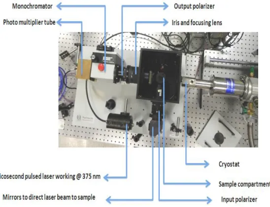
Figure 2.3.1.1 FluoTime 200 time resolved fluorescence spectroscopy system used for time resolved measurements in this thesis. ... 27
Figure 3.1.1 Colloidally synthesized nanocrystal quantum dot with surface passivating ligands attached to surface Cd atoms are shown representatively. .. 33
Figure 3.1.2 Schematical examples of type I and type II core/shell NQDs. ... 35
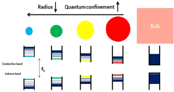
Figure 3.2.1. Schematic representation of semiconductor NQDs , along with its bulk, showing modified electronic band structures due to quantum confinement. ... 38
xiii
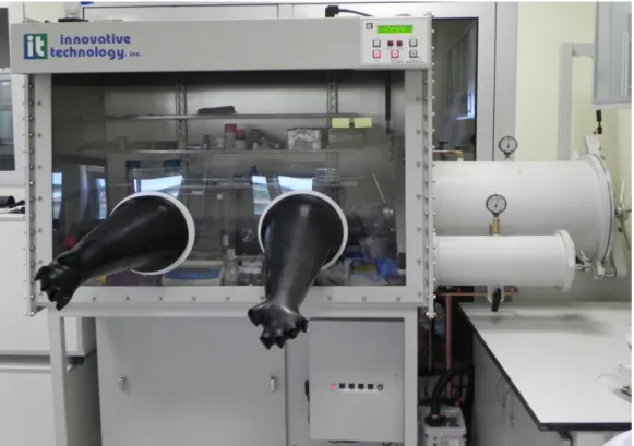
Figure 3.3.1 Synthesis set-up consisting of Schlenk line for Argon flow and vacuum. Cold trap is utilized for vacuum line. Oxygen absorber is utilized for making oxygen free Ar flow. ... 39 Figure 3.3.2 Glove box filled with nitrogen to create oxygen free environment
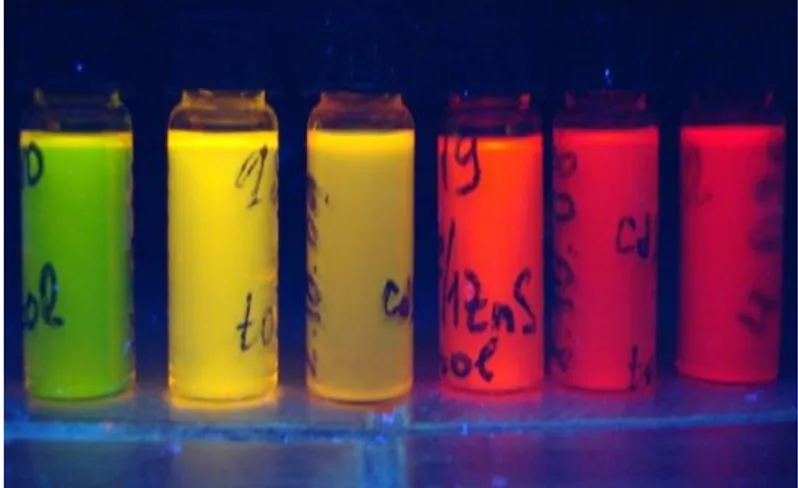
for oxygen sensitive material processing. ... 40 Figure 3.3.3 Our-synthesized CdSe core and CdSe/ZnS core/shell NQDs with
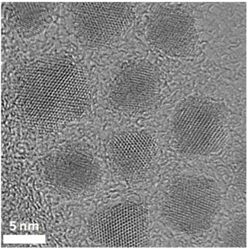
different sizes emitting at correspondingly different wavelengths. ... 41 Figure 3.4.1. Photoluminescence and absorbance of CdSe/ZnS NQDs having different sizes (the largest particles has red emission, while the smallest has green emission). ... 43 Figure 3.4.2 Highly monodisperse CdSe/ZnS NQDs. ... 44 Figure 3.4.3 High resolution TEM image of CdSe/CdSe-CdS-ZnS/ZnS alloy
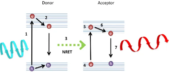
like core/shell NQDs having PL QEs around 80%. ... 45 Figure 4.2.1 Exemplary experiment for the demonstration of the presence of NRET. ... 50 Figure 4.2.2 An oscillating Hertzian dipole is shown with electric field radiation patterns in the near-field. ... 51 Figure 4.2.3 Schematic of the principle of operation of NRET between donor
and acceptor luminescent molecules. ... 53 Figure 4.2.4 Jablonski energy diagram of a luminescent organic molecule with
possible de-excitation pathways. ... 56 Figure 5.1.1 Typical architecture of a planar crystalline silicon solar cell. Short wavelength (highly energetic) photons are absorbed very close to the silicon surface... 61 Figure 5.1.2 Examplary external quantum efficiency vs. wavelength of a silicon
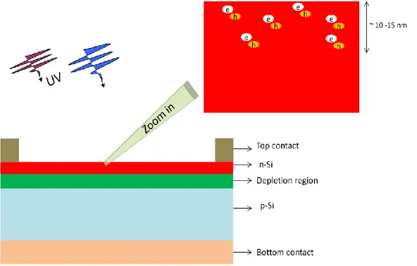
nanowire solar cell used in this study. ... 62 Figure 5.2. 1 Illustration of the principles of operation of the nanocrystal up-converter layers for silicon solar cell. Comparison of the planar and nanopillar architecture is pictorially presented. UV and blue waves are shown as the excitation photons. Orange colored waves represents the longer wavelength
xiv
emission of nanocrystals after conversion of UV and blue photons. Black
colored arrows represents the built-in electric field in depletion region. ... 63 Figure 5.2.2 Absorption (black line) and emission spectrum (red line) of the
utilized CdSe nanocrystals. ... 64 Figure 5.3.1 Scanning electron micrographs for fabricated radial p-n junction Si nanopillar solar cell are shown. The device architecture is also depicted.
Photograph of the active device is given, where device active area is ~ 0.81 cm2. ... 67 Figure 5.3.2 Transmission electron micrograph of synthesized CdSe
nanocrystals (scale bar is 5 nm). ... 68 Figure 5.3.3 SEM images of silicon nanopillars after nanocrystals are
incorporated... 69 Figure 5.3.4 Current-Voltage (I-V) curves of the nanopillar solar cell before and
after nanocrystal incorporation under AM 1.5G 1sun illumination
conditions. ... 71 Figure 5.3.5 Enhancement in responsivity due to nanocrystal hybridization in
planar and nanopillar solar cell devices is presented. Inset shows external quantum efficiencies of the nanopillar and planar devices before and after nanocrystal incorporation... 72 Figure 5.3.6 Measured reflectivity of silicon surface with and without
nanocrystal coating. ... 73 Figure 5.3.7 FDTD analysis of reduction of the reflectivity and enhanced light
trapping of nanopillar silicon solar cell due to nanocrystal incorporation. Inset shows the measured reflection (%) before and after nanocrystal incorporation. ... 74 Figure 6.1.1 Color converter light emitting diodes can benefit NQDs as optically active converting materials. Combination of different color emitting NQDs can be used to generate white light... 78 Figure 6.1.2 A similar pump LED and a monolayer of CdSe NQDs used by
Achermann et al. where they etched GaN capping layer in order to decrease the seperation between top QW and monolayer of the NQDs. [83]... 79
xv
Figure 6.2.1 NQDs elliptically etched holes (a) reaching down to QWs, (b) lying only in p-GaN capping layer. [84] (This figure is reproduced with
permission of the publisher John Wiley & Sons Inc.) ... 80 Figure 6.2.2 InGaN/GaN multi-quantum-well nanopillars obtained via
inductively plasma reactive ion etching (ICP REI). Inbetween pillars are incorporated NQDs. ... 82 Figure 6.3.1 Explanatory schematics for the fabrication of InGaN/GaN MQW nanopillar structures. ... 83 Figure 6.3.2 SEM image of the top-down fabricated InGaN/GaN MQW
nanopillars. ... 84 Figure 6.3.3 X-ray diffraction measurement of the nanopillars (blue) and planar
(black) architecture. ... 84 Figure 6.3.4 (a) Photoluminescence spectra of InGaN/GaN multi-quantum-well
planar (black) and nanopillar (blue) structures, and (b) time resolved fluorescence decays for planar (black) and nanopillar (blue). ... 86 Figure 6.3.5 In-solution PL and absorbance spectra of the utilized CdSe/ZnS
NQDs in this part of the thesis. Emission of the planar and nanopillar LEDs are also shown to indicate the spectral overlap between the donor emission and the acceptor absorption... 88 Figure 6.3.6 (a) Time resolved fluorescence decays of multi-quantum-wells in
nanopillar architecture with and without red NQDs along with exponential fits. (b) Steady state PL spectrum of the nanopillar NQD hybrid usin red NQDs. ... 91 Figure 6.3.7 (a) Time resolved fluorescence decays of multi-quantum-wells in
nanopillar architecture with and without green and yellow NQDs along with their fit exponential fits. (b) Steady state PL spectra of the nanopillar NQD hybrids using yellow and green NQDs. ... 92 Figure 7.2.1 Five different vials containing functionalized polyfluorene (PF) derivative co-polymer emitting in blue and our own-synthesized core/shell
xvi
NQDs of different sizes and emission wavelengths (green to orange).
Functionalized PF is depicted as donating its excitons to the NQDs. ... 101 Figure 7.2.2 Schematic of the QD-LED device architecture with the actual
photograph of a fabricated device. ... 102 Figure 7.2.3 Schematic for the principle of operation of the exciton pumped
QD-LEDs where electrons „-‟ and holes „+‟ are injected from cathode and anode, respectively. Also, red dots represent the hybridized NQDs. Due to finite mobility of the charges in the polymer matrix, they are combined to form excitons, which can be effectively transferred to the NQDs via
nonradiative energy transfer. ... 102 Figure 7.3.1 Schematic depiction of phase segregation between NQDs and polymer. ... 104 Figure 7.3.2 Carboxyl group functionalized polyfluorene derivative co-polymer.
... 106 Figure 7.3.3 Non-functionalized polyfluorene derivative co-polymer used as a
negative control group. ... 106 Figure 7.3.4 SEM images of thin films of (a)-(d) NQDs with non-functionalized
PF blends shown with material EDAX analysis of the segregated parts of the films in (d), and (e) NQDs with functionalized PF hybrids. ... 109 Figure 7.3.5 Atomic force microscopy images of non-functionalized PF-NQD
blends: (a) topography, and (b) phase image. ... 110 Figure 7.3.6 STEM images of NQDs in (a) functionalized PF and (b)
non-functionalized PF. ... 113 Figure 7.3.7 In-solution (a) and in-film (b) absorption - emission spectra of
functionalized PF shown along with the absorption spectrum of NQDs.. 114 Figure 7.3.8 (a) Lifetimes of the functional PF in the presence and absence of
the quantum dots for 3 w% and 45 w% hybrids with respect to temperature. (b) Energy transfer efficiencies extracted from LAF model with respect to temperature for 3 w% and 45 w% cases. ... 119 Figure 7.3.9 NRET rates for 3 w% and 45 w% hybrids with respect to
xvii
Figure 7.3.10 Iso-efficiency curves with respect to D vs. nA and LD vs.
Acceptor-acceptor separation for (a) 3 w% and (b) 45 w% hybrids.
Semitransparent pink regions indicate the possible regions for D and LD for
predicted nA and NQD separations in thin film. ... 124
Figure 7.3.11 One dimensional schematic interpretation of the exciton diffusion in polymer in relation to NRET dynamics. ... 128 Figure 7.3.12 Steady state PL for only polymer and hybrid at different
temperatures [PLs should be corrected with the correction factor. ... 130 Figure 7.3.13 Amplitude averaged acceptor lifetimes for (a) 3 w% and (b) 45
w% at each temperature and sample measured for its peak emission
wavelength. ... 132 Figure 7.3.14 Exemplary lifetime decays of donor alone, 3 w% and 45 w% with
IRF at room temperature. ... 133 Figure 7.4.1 Schematic representation of the fabrication steps of the QD-LEDs following the fabrication steps 1-8. Photograph of a fabricated and encapsulated device is also shown. ... 135 Figure 7.4.2 Examplary electroluminescence of a QD-LED made up of
non-functionalized PF and core/shell NQDs... 136 Figure 7.4.3 EL spectrum of excitonically driven QD-LEDs prepared with
increasing concentration of NQDs and only polymer–LED at same voltage level with normalized EL spectra. ... 137 Figure 7.4.4 Typical I-V curve for the excitonically driven QD-LEDs fabricated with functionalized PF and red emitting CdSe/ZnS NQDs. ... 138 Figure 7.4.5 Luminance – current (LI) measurement of the fabricated
excitonically QD-LED consisting of functionalized PF and red emitting CdSe/ZnS NQDs. ... 139 Figure 7.4.6 EL spectrum of excitonically injection pumped QD-LEDs utilizing
different color emitting NQDs. ... 140 Figure 7.4.7 EL spectrum of excitonically driven QD-LED with functionalized
PF and green emitting CdSe/CdS/ZnS NQDs designed for obtaining pure green emission. ... 141
xviii
Figure 7.4.8 Cyclic voltammetry measurement of functionalized PF in order to determine its highest occupied molecular orbital level (HOMO). ... 142 Figure 7.4.9 External quantum efficiency vs. injected current for a QD-LED
xix
List of Tables
Table 5.3.1 Evolution of solar cell parameters before and after incorporation of nanocrystals. ... 70 Table 6.3.1 Total decay rate for nanopillar alone and energy transfer rates, efficiencies and percent of transferred electron-hole pairs for red, orange and yellow emitting NQDs incorporated into nanopillars are shown………94 Table 6.3. 2. Experimental and theoretical energy transfer rates are compared.
Other parameters used for the calculation of the theoretical rates are also given (J, n, d, and σ)………96
xx
1
Chapter 1
Introduction
1.1 Motivation of the Thesis
In today‟s world, energy production and utilization became a vital problem of the human society. Environment-unfriendly means of energy production escalate the global warming. Inefficient utilization of energy in lighting, transportation, heating, etc. also causes significant loss of effort and sources. Scientific community is challenged to develop better ways of production and utilization of the energy.
Optoelectronic devices such as photovoltaic solar cells and light emitting diodes offer possible competent solutions to the problems of energy. Today, luminescent semiconductor nanocrystal quantum dots arise as a unique and novel material class, holding great promise to be harnessed for optoelectronics technology for excelled devices. To this end, we propose and show enhancement of photovoltaic solar cells and light emitting diodes via hybridization of semiconductor nanocrystal quantum dots while promoting and mastering their radiative and nonradiative energy transfer capabilities.
According to U.S. Energy Information Administration, 12% of the residential and 25% of the commercial (e.g., industry, government) electrical consumption in U.S.A is due to lighting. [1] According to another report, approximately 19% of the total electricity production on earth is used for lighting purposes. [2]
2
Although a huge portion of the produced electricity is used for lighting, incandescent and fluorescent lamps still make the main means of lighting, which are not quite efficient as compared to the light emitting diodes. Incandescent lamps provide poor luminous efficiencies (lm/W) around 10-20 lm/W with short lifetimes up to 1000 hours. [3] Fluorescent lamps, which can be as efficient as 30 - 80 lm/W, feature lifetimes limited to at most 10,000 hours. [3] However, light emitting diodes can offer both high efficiencies around 30-100 lm/W and increased lifetimes more than 30,000 hours. [3] Year by year, LED market grows faster. In 2006, the market was valued to be 4 billion USD. Predictions for 2015 expect the LED market to grow 15 billion USD. [4] Wide application areas of LEDs such as display technology, automotive and general lighting contribute to this rapid growth of the LED market. Although there have been many advancements in the LED technology, the pursuit of better and more efficient devices still continues.
In the-state-of-art LED technology, color converter layers are typically used to obtain white light. [5] In display applications, Red-Green-Blue (R-G-B) colors can also be obtained via color conversion method. Color converter layers generally employ rare-earth doped phosphor materials. However, these phosphors limit the optical quality of the LEDs since their emission spectrum cannot be tuned and controlled easily. Novel luminescent quantum dot nanocrystals are promising and interesting materials showing competitive advantage to be used for color converter layers. [6] These quantum dots are promising candidates to replace phosphor based converter layers in the future. [7] In this thesis, we focus on the utilization of these novel luminophore quantum dot nanocrystals as efficient color converter layers for novel nanostructured LEDs to harness increased nonradiative energy transfer mechanisms between the pump LED and quantum dot nanocrystals. The pump LED is also nanostructued to exploit the nonradiative energy transfer means effectively.
3
Rising field of organic optoelectronics draws a great attention owing to its advantages such as low cost production of versatile devices even on flexible substrates with the ease of production methods such as solution processing. Hybrid systems based on quantum dot nanocrystals and organic materials can combine the superior properties of both material systems. Hybrid quantum dot based LEDs have been proposed to be promising devices for display applications. [8, 9] However, due to poor electrical properties and high potential barrier on the ligands of the colloidally synthesized quantum dot nanocrystals, charge injection problems exist in these devices. In this thesis, we propose and present a proof-of-concept demonstration of excitonically pumped quantum dot based hybrid LEDs. We investigate the dynamics of exciton injection that is achieved via nonradiative energy transfer from conductive polymers to quantum dot nanocrystals. Exciton injection scheme is a novel approach which can be utilized as an alternative method for electroluminescent nanocrystal-based LEDs.
Convenient energy production means are fossil fuels such as coal, natural gas, petroleum and nuclear sources which are not quite nature friendly. Burning fossil fuels causes increased greenhouse gas emission, which has contributed to the accelerated global warming problem in the previous century. Emission of the greenhouse gases should be cut down to preserve our living habitat. Alternative and clean energy sources are welcomed today with the support of international communion. Photovoltaic (PV) solar cells are one of the most promising candidates as alternative and clean energy sources primarily because enormous potential of the Sun, although there are cost issues for wide scale use. The Sun delivers on the average 89,000 TW power instantly to earth crust, which is three orders of magnitude greater than the worldwide energy consumption of about 15 TW. [10] If we were to compare the potential of the Sun with other energy sources on earth, we would see that the annual solar irradiation energy impinging earth is a few orders of magnitude greater than the potential of the individual energy sources on earth (e.g., coal, natural gas). [11] Examples of the
4
potential of solar energy are stunning. If we were to cover two thirds of Sahara desert with commercially available 15% efficient silicon solar panels, then all of the energy demand of the world could be only met by solar means. Also, if we were to cover roof tops of the buildings in Antalya, then almost 18% of the energy demand of Turkey could be met by those solar panels. [12] However, there exist feasibility problems due to economical and production related issues. Today‟s PV technology has a limited capacity of production so that covering some part of Sahara with 15% efficient modules will take almost 100 years of production. Although alternative solar cell technologies except silicon has been developed such as organic solar cells offering the ease of roll-to-roll fabrication methods, silicon is still the dominant material in PV technology. [13] This is because material processing technologies for silicon are quite mature thanks to developments in micro-fabrication technologies. Silicon is also one of the most abundant materials on earth. Nevertheless, due to intrinsic properties of silicon, optoelectronic devices such as photo-detectors and solar cells suffer from poor UV and blue light responsivities. For photovoltaic applications, poorly utilized UV and blue spectra constitutes almost 10 % of the total spectrum of the sun light. In this thesis, we propose the utilization of novel luminescent quantum dot nanocrystals as wavelength up-converter layers so that UV and blue photons in sun light will be harvested better by silicon solar cells. To benefit this color conversion approach, nanostructured silicon solar cell is utilized because of unique optical trapping properties.
1.2 Organization of the Thesis
This thesis consists of eight chapters. Here is the organization of the rest of the thesis. In Chapter 2, we review the theory and experimental methods related to the scientific content of this thesis. In Chapter 3, novel luminescent quantum dot nanocrystals are presented in detail including the theory of the quantum confinement. Here we also explain the synthesis of these quantum dots. Subsequently, possible applications are summarized. In Chapter 4, we discuss the physics of radiative and nonradaitive energy transfer mechanisms. Quantum
5
dot based application examples are also provided. In Chapter 5, we present our study on enhanced silicon nanopillar radial p-n junction solar cells via radiative energy transfer from quantum dot nanocrystals utilized as wavelength down-converters of UV-blue photons in the sunlight. In Chapter 6, we investigate the utilization of nanopillar InGaN/GaN multi-quantum-well pump LEDs as efficient energy donors for color converter layers made up of quantum dots. The physics and dynamics of energy transfer are studied both experimentally and theoretically. Results of the proof-of-concept hybrid devices are presented. In Chapter 7, we present our proposal of novel exciton injection pumping scheme for electroluminescent quantum dot nanocrystal based LEDs. Hybrid material system of nanocrystals and functionalized polymer that is proposed to achieve exciton injection is explained. Temperature dependent exciton transfer dynamics are investigated using time resolved fluorescence measurements. Physical model are discussed. The proof of concept devices are also presented. Last, in Chapter 8, we conclude the thesis with remarks on the completed projects and future steps.
6
Chapter 2
Scientific Background
2.1 Photovoltaic Solar Cells
2.1.1 Principles of Operation
Although there are different generations of solar cells based on various material systems, the fundamental principle of operation is the same for all generations of devices. The main goal of a photovoltaic solar cell is to convert the sunlight into electricity. Semiconductor materials are the most appropriate material class to be utilized for photovoltaics because of available energy band gaps tunable in the spectra of the sunlight. Absorption of a photon by semiconductor material causes creation of an excitation energy carrier called electron hole (e-h) pair in the material. The principle of operation of the photovoltaic devices depends on the separation of the created e-h pairs in the p-n junction so that photocurrent is generated in the external circuit. For this reason, solar cells act as current sources.
The first generation solar cells use only single p-n junction diodes made up of single crystalline silicon as the active absorbing material. The first generation devices are still popular since they can provide respectively high power conversion efficiencies despite the high production costs due to utilization of high quality single crystalline silicon substrates. [14] The second generation devices also called thin film solar cells have been introduced against the first
7
generation devices to reduce the costs via utilization of very thin semiconductor compound or alloy materials. Common materials used for the second generation photovoltaics are amorphous silicon (a-Si), cadmium sulfide/cadmium telluride (i.e, CdS/CdTe) and copper indium gallium di-selenide (i.e., CIGS). However, these devices are generally limited with relatively low power conversion efficiencies due to poor absorption of the sunlight in thin films.
Newly emerging third generation solar cells based on several different approaches such as organic conductive materials, conductive oxides with dye sensitization, optical concentrators, multi junctions, carrier multiplication (i.e., multiple carrier generation), hot carrier collection, quantum dot sensitization, IR utilization, and nano-structured light trapping. The physics, chemistry and materials may change a lot, but the operation principle still follows the basic photovoltaic effect of e-h pair photogeneration and dissociation and subsequent charge collection.[15] It is also worth noting that there are differences between various photovoltaic devices in terms of how a photogenerated e-h pair is dissociated (e.g., through built-in field, acceptor-donor interaction).
To give a detailed picture of the principle of operation of photovoltaic solar cells, a simple p-n junction diode would be the easiest to understand. Here we depict a p-n homojunction diode under light illumination with a photon energy larger than the band gap of the utilized semiconductor material (see Figure 2.1.1.1). Although there are a huge number of electrons in a semiconductor material, most of them are bound to atomic nucleus, so called valence electrons, which are incapable of moving the crystalline material freely. If some of the electrons gain energy due to excitation (i.e., photon absorption or electrical injection), then excited electrons in the valence band would move freely in the conduction band. Empty states in the valence band by excited electrons are then called holes, virtual positively charged mobile charge carriers. Both electrons and holes can contribute to conduction in a semiconductor material. In a n-doped material, there are a lot of free electrons that constitute the majority
8
carriers and there are positively charged immobile dopant atoms (see Figure 2.1.1.1) (i.e., since they have donated their electrons). In a p-doped material, conversely, there will be a lot of free holes that are the majority carriers and there are negatively charged immobile dopant atoms (see Figure 2.1.1.1). Minority carriers (i.e., holes for n-doped, electrons for p-doped) can only be created in the material due to either photo-generation, thermal excitations or reverse biasing. These minority carriers play a quite important role in the operation of p-n junction solar cells for the generation of the photocurrent.
Figure 2.1.1.1 Schematic representation of a p-n junction diode. Material is excited with photons in the visible range. Photogenerated electron-hole pairs are represented. Due to doping of the material resulting immobile ionized acceptors and donors along with free electrons and holes are
shown. Energy vs. position schematic shows the alignment of the p- and n-doped regions with depletion region where built-in electric field exists.
Photons having energy greater than the band gap energy will have a chance to be absorbed by the material. As a consequence of photon absorption, in either
n-9
doped, p-doped or depletion region of the material, electron-hole pairs will be created (see Figure 2.1.1.2). Minority carriers have a limited lifetime in the doped regions, since recombination with a majority carrier is likely to happen. However, in this limited duration of the minority carrier lifetime, minority carriers should be carried towards the junction (see Figure 2.1.1.2 – process 1,2). Diffusion is the dominant process for the motion of minority carriers toward the junction. When a minority carrier reaches the junction (i.e., depletion region), then due to strong built-in electric field in the junction, minority carriers are drifted towards the opposite region where they are already majority carriers (see Figure 2.1.1.2 – process 3-4). When a minority carrier becomes a majority carrier due to drift current in the depletion region, this creates a current in the external circuit as shown in Figure 2.1.1.2 (process 5-6).
Figure 2.1.1.2 Principle of operation of a solar cell is depicted. Electron and hole pair is created via photo-generation. A minority carrier (e.g., a hole in this case) diffuses in the region (1, 2). If it can reach the junction (i.e., depletion region) after diffusing (3), it is drifted to the other region
where it is majority carrier (4). Due to this drift current, in the external circuit, the majority carrier (e.g., electron in this case) is given to external circuit (5) so that it recombines with a
10
2.1.2 Important Device Parameters and Characterization
Techniques
There are basically four important parameters related to characterization of solar cells: Short circuit current (Isc), open circuit voltage (Voc), fill factor (FF) and
power conversion efficiency. Spectral response related parameters as spectral responsivity (R(λ)) and external quantum efficiency (EQE(λ)) reflect the important spectral properties of the devices.
Short circuit current, as its name implies, is the current driven in the external circuit in the absence of any load due to photo-generation as shown in Figure 2.1.2.1. Isc is the maximum attainable current that a solar cell can supply.
Because any load attached to the external circuit will cause a positive bias on the p-n junction, which will reduce the photocurrent due to increase in the oppositely signed diffusion current in the devices caused from reduced built-in electric field. However, a photovoltaic device cannot be operated under short circuit conditions since no power can be supplied to the external circuit. The parameter, short circuit current, depends on a few factors: optical light power intensity, spectrum of the light, and optical and electrical properties of the device. Short circuit current is a negative current since it flows in opposite direction to the forward biased current (see Figure 2.1.2.1). Since short circuit current is negative, current-voltage characterization of solar cells is undertaken in the fourth quadrant of I-V curve (current in y axis, voltage in x axis) (see Figure 2.1.2.3).
11
Figure 2.1.2.1 Short circuit current mode of a p-n junction solar cell.
Under light illumination, open circuit voltage is the voltage difference between two terminals of the p-n junction solar cell with no current flow. This voltage build-up across a p-n junction due to photo-generation is explained by the photovoltaic effect. The photo-generated electron-hole pairs that drift in opposite directions across the depletion region due to the built-in field (see Figure 2.1.2.2) creates an electric field of their own through the diode in an opposite direction to the built-in electric field. The resulting reduction of the built-in electric field in the depletion region also increases diffusion currents since barrier against electrons in n-doped region to pass p-doped region is reduced (the same happens for holes in the p-doped region to diffuse into n-doped region). Also reduced built-in electric field decreases the drift currents. Since direction of the diffusion current and drift current is opposite, when drift currents are equalized with the diffusion currents due to increased photo-voltage, net current becomes zero. This condition is called open circuit voltage where as similar to short circuit current case, there is no net power generation. Although short circuit current depends on factors related to optical light intensity, open circuit voltage is more related to internal structure and material
12
properties of the device. It depends on recombination dynamics and dark current of the device along with the amount of built-in electric field.
Figure 2.1.2.2 Open circuit mode operation of a p-n junction solar cell.
Fill factor is a measure of maximum power generation capability of a solar cell. Since solar cells are not made up of ideal diodes, current-voltage (I-V) characteristics does not follow ideal diode behavior. Then, fill factor (FF) is the ratio of the area under the square defined by the actual maximum power point (IMPP and VMPP) and the square defined by the ideal maximum power point (ISC
and VOC) (see Figure 2.1.2.3). FF is given by (2.1.2.1).
(2.1.2.1)
As can be seen from an exemplary I-V curve, Isc, Voc, IMPP, VMPP, PMax and
13 0.0 0.2 0.4 0.6 -0.012 -0.008 -0.004 0.000 0.004 0.008 Pmax_ideal VMPP IMPP Pmax ISC I-V curve
Power curve (IxV)
C u rr e n t (A ) Voltage (V) VOC
Figure 2.1.2.3 Exemplary I-V curve of a silicon solar cell studied in this thesis. Important solar cell parameters, Isc, Voc, Pmax, Pmax ideal, Vmaximum power point and Imax power point are shown on I-V and
power – voltage plots.
Power conversion efficiency factor is one of the most important figure-of-merits for solar cells. It is physically defined as the ratio between maximum electrical output power and optical input power as given in ( 2.1.2. 2).
( 2.1.2. 2)
Power conversion efficiencies are determined using a universal standard called one sun - Air Mass 1.5 Global Solar Spectrum (AM 1.5G), which is the measured spectra of sunlight on earth surface on a bright sunny day with a power intensity of 100 mW/cm2. To produce AM 1.5G spectra with desired power intensity, specially designed solar simulators are utilized. These produce wide emission spectra illumination using a Xenon-arc lamp and with the help of optical filters designed specifically for imitating the spectra of sunlight,
14
AM1.5G conditions can be satisfied. A calibrated solar cell is used to correct the power intensity levels of a solar simulator system.
Another characteristics of a solar cell is the wavelength dependent characteristics the so-called spectral responsivity (in units of A/W) or external quantum efficiency (# of electrons out / # of photons in). These spectral properties can be measured with a spectrometer set-up as shown in Figure 2.1.2.4. A monochromator picks desired emission wavelength from the wide emission spectra of the Xenon lamp. A lock-in amplifier works in harmony with the optical chopper in order to reduce the noise due to any light in the environment by making modulated optically chopped measurements. We also measure the optical power levels in the measurement spectrum via an optical powermeter by placing the powermeter detector instead of the sample. Spectral responsivity can be obtained by simply dividing the measured currents by the measured spectral optical power levels. There is a strong relation between the spectral responsivity (R(λ)) and the external quantum efficiency (EQE). We can calculate spectral EQE using ( 2.1.2. 3) where hν is the photon energy and e is unit charge.
( 2.1.2. 3)
Figure 2.1.2.4 Measurement set-up for wavelength dependent responsivity and external quantum efficiency.
15
Figure 2.1.2.5 shows an exemplary spectral EQE of a silicon p-n junction solar cell. In the visible region, this device exhibits a high EQE. However, at both ends of the spectra, EQE tends to decrease. The decrease in UV part is due to strong absorption of the photons close to the top surface of the device so that these created e-h pairs cannot contribute to the drift current since minority carriers recombine at high surface trap states. In the IR region, EQEs are again reduced due to decreasing absorption coefficient of silicon.
Figure 2.1.2.5 Exemplary external quantum efficiency plot for a silicon based solar cell. EQE is low at both ends of the spectrum. In the UV part, it is low due to poor utilization of electron-hole
pairs close to the surface. In the IR part, it is low due to poor absorption of silicon with back contact problems. [16]
2.2 Semiconductor Light Emitting Diodes
2.2.1 Principles of Operation
Most of the direct band gapsemiconductor materials having band gap energies matching with the electromagnetic spectrum of light (i.e., UV to IR) are known to possess fluorescence properties. When excited with a light source having
16
photon energy larger than the band gap of the semiconductors, electron-hole pairs are photo-generated. Due to radiative recombination properties of semiconductor materials, these electron-hole pairs can recombine to give their excess energy in the form of photon emission. Electroluminescence (EL) is the principle of operation of light emitting diodes where electrically injected charges are combined to form electron-hole pairs so that radiative recombination results in emission of photons. Conversely to solar cells, where photo-generated electron-hole pairs are extracted into external circuit, here in LEDs electrons and holes are injected into the junction and subsequently, they recombine to emit photon.
The main principle of operation of LEDs is summarized schematically in Figure 2.2.1.1. Under zero bias, a p-n junction diode has a structure and energy diagram as shown in Figure 2.2.1.1 (a). However, if we apply a positive forward bias, charge carriers will be injected from respective contacts (i.e., electrons from n-doped region and holes from p-n-doped region) (see Figure 2.2.1.1 (b)). Those charge carriers will perturb the carrier balance in doped regions so that quasi Fermi levels will be formed (i.e., Efn and Efh). Injected carriers will diffuse in the
material towards the junction. Built-in electric field is reduced due to forward bias, then charges will have less hinderence to move through the junction. Some of the electrons and holes will combine together to form bound electron hole pairs so that they will either radiatively or nonradiatively recombine depending on the internal luminescence properties of the material.
17 (a)
(b)
Figure 2.2.1.1 (a) A p-n homojunction diode under zero bias is shown with free electron and holes in n- and p-doped regions, respectively. (b) A p-n homojunction diode under forward bias is shown. Built-in electric field is reduced. Diffusion current increases. Quasi-Fermi levels form
due to injection. Formed electron-hole pairs can emit light (i.e., electroluminescence).
Today, LED technology utilizes direct band gap epitaxially grown compound semiconductor materials such as GaAs, AlGaAs, GaP and AlGaInP for IR and red emitting diodes; GaN, InGaN and GaAsP for yellow and green emitting diodes; InGaN, ZnSe and AlGaN for blue and UV emitting diodes. These
18
materials are generally grown by metalorganic chemical vapor deposition technique which is quite expensive and slow compared to deposition methods of colloidal particles and organic polymers and molecules.
2.2.2 Organic Light Emitting Diodes
There are alternative approaches to all inorganic LEDs such as organic light emitting diodes (OLEDs), which utilize luminescent and conductive organic materials. OLED technology provides cheaper and versatile devices with ease of fabrication techniques. Conjugated polymers which were invented in late 70‟s have undergone many developments in the last decades and a new technology based on these materials emerged. Their inventers were awarded with a Nobel prize in 2000.
Due to π-π*
bond stacking, band-like electronic and optical properties are observed for conjugated polymers (see Figure 2.2.2.1). Formation of the highest occupied molecular orbital (HOMO) and the lowest occupied molecular orbital (LUMO) resembles valence and conduction band properties of the inorganic semiconductor materials. The energy difference between HOMO and LUMO is the effective band gap of the polymer. Although their electrical properties are poorer as compared to mono-crystalline highly doped semiconductor materials, these organic counterparts provide advantages such as ease of processing methods with novel mechanical properties, which make them very promising materials for future optoelectronic applications. Solar cells, light emitting diodes, lasers and transistors made up of all organic means have been already shown. [17, 18, 19, 20]
19
Figure 2.2.2.1 A typical band diagram of a conjugated polymer where LUMO level corresponds to conduction band and HOMO level to valence band.
The similar principle of operation for inorganic LEDs also applies to OLEDs, which simply relies on the electroluminescence under current injection. The whole visible spectrum can be covered with different conjugated polymer types having different band gaps. These novel semiconductor materials have been observed to make good electrical contacts with metal interfaces. Although charge mobility in these materials are not so fast, this does not create a main drawback for LEDs; however, this might be a problem for laser applications where very fast electron-hole pair formation is required. A side note should be given here that, in the context of organic materials, electron-hole pairs are not articulated much, since organic materials are known to have strongly bound excitation carriers, the so-called excitons (i.e., Frenkel excitons) with binding energies more than a few hundreds meV. A polymer based OLED can be designed in its simplest form in a single layer architecture as shown in Figure 2.2.2.2. Generally low work function metals such as Ca and Mg and their combinations with other relatively low work function metals Ca/Al, Mg/Ag, etc, are used to make top contacts. These top contact serve as cathode so that electrons are injected. The bottom electrode is chosen to be transparent since light extraction to external world should take place. Most popular transparent conductive oxides (TCO) are indium tin oxide (ITO) and fluorine doped tin oxide (FTO). TCOs are used as anodes (i.e., hole injection). ITO is far most popular TCO since ITO provides a better work function match with commonly used polymer‟s HOMO levels for hole injection. Injected electrons and holes are
20
combined in the polymer to form excitons, subsequent to exciton formation emission of a photon takes place.
Figure 2.2.2.2 The simplest device design for polymer based OLED. Top contact is used as cathode and bottom contact is used as anode.
We have drawn the band diagram of the simplest polymer OLED design as shown in Figure 2.2.2.3 to understand the EL properties of the devices. At zero bias, there will be no potential difference between the anode and cathode, and charges cannot be injected (Figure 2.2.2.3 (a)). At increased forward bias levels, we will first reach a threshold voltage after which injection will start immediately (Figure 2.2.2.3 (b)). At higher bias levels, charge could be injected into polymer through tunneling from cathode and anode (Figure 2.2.2.3 (c)). Injected charges would then meet each other to form excitons in the polymer.
(a) (b) (c)
Figure 2.2.2.3 Three different bias conditions for simple device design of sandwiched polymer layer between anode and cathode. (a) At zero bias charges cannot be injected. (b) At threshold
21
forward bias level, charge injection becomes possible (immediately after this bias level). (c) At bias levels greater than threshold, charge injection can take place via tunneling.
For polymers emitting in red, yellow and green, the offset energy between anode and cathode work function is not significantly high, so that injection can be still effectively achieved via tunneling. However, for large band gap blue emitting polymers, energy offsets between work function of the contacts and HOMO or LUMO levels of the polymer may reach about 1 eV, which significantly reduces the device efficiencies due to poor charge injection. Better designs are required to make charge injection more efficient and balanced; also, charge confinement in the active layer would help to form more excitons in the active emission layer. Use of injection, transport and blocking layers are ideally utilized in a more advanced design as shown by Figure 2.2.2.4. In this kind of an OLED design, quite efficient devices can be obtained. Electron and hole injection layers reduce the mismatch between metal and the first organic layer. Injected carriers are then transferred to transport layers which can have high conduction properties for a given charge carrier type. Carrier blocking layers help to block the other type of charge carrier due to large difference in HOMO or LUMO levels between the active layer and the block layer. When charge carriers are injected into polymer active emission layer, excitons will be formed. Exciton formation probabilities are increased because of blocking layers providing confinement of charges in the active layer.
22
Figure 2.2.2.4 An advanced design for an efficient OLED.
Except conjugated polymers, small organic fluorescent molecules can also be used as the active emitting layers. Most of the injection, transport and blocking layers consist of small organic molecules, which are generally coated via thermal evaporation techniques. When these molecules are heated to moderate temperatures such as 300- 400oC under vacuum, molecules tend to evaporate without breaking into atoms so that controlled films can be easily achieved. However, solution processing is also possible, which is quite inexpensive, and an easy method of spin coating or similar cheap and straightforward methods are utilized. One of the vital advantages of organic materials is that they can be coated on flexible substrates, allowing for roll-to-roll processing, since they have ductile material properties unlike crystalline inorganic materials. In the future, wearable devices could become possible with the developments in organic optoelectronics.
23
2.2.3 Important Parameters and Characterization
Light emitting diodes are mainly characterized with several measurement techniques. Electrical properties are mainly studied with current-voltage (I-V) measurements. Luminosity-current (L-I) measurements can be made to understand the relation between injected current levels and number of output photons to specify the stable operation regions. Electroluminescence (EL) spectrum measurements are also performed to observe the EL spectra of the devices under different bias and current levels. Some important device parameters are turn-on voltage, luminous efficiency (LE), and external quantum efficiency of the devices.
An exemplary I-V curve of an OLED is shown in Figure 2.2.3.1. I-V data is useful to understand the electrical properties of the LEDs since directly turn-on voltage and injection related properties can be analyzed through I-V curves. A parameter analyzer is typically utilized to measure the I-V relation of the diode.
-1 0 1 2 3 4 5 6 0.000 0.001 0.002 0.003 0.004 0.005 C u rr e n t (A ) Voltage (V)
Exemplary I-V curve
24
In order to determine the L-I (luminosity-current) property of a LED, optical power meter can be used. We also utilize an integrating sphere to collect emission of the LEDs in all direction An example L-I data of an OLED is shown Figure 2.2.3.2. L-I data is useful to understand the operation limits of the devices. For example, after driving higher current through a device, L-I curve does not follow a linear relation due to heating problems of the LEDs, which can severely reduce the efficiencies.
4 5 6 7 8 9 400 500 600 700 800 900 1000
O
p
ti
ca
l p
o
w
er
(
a.
u
.)
Current (mA)
Exemplary LI dataFigure 2.2.3.2 An exemplary LI data of an OLED.
Another important characterization is the measurement of EL spectrum. An exemplary EL spectrum of an OLED is shown in Figure 2.2.3.3. EL spectrum can be easily measured using a charge-coupled-device (CCD) integrated spectrometer (Ocean Optics 2000) connected to a optical fiber, which is attached to the integrating sphere where sample is electrically excited. EL spectrum is quite important since one of the most important specifications of the LEDs is their EL spectra. EL data can be taken at different charge injection levels to check spectral stability of the devices.
25 400 450 500 550 600 650 0 30 60 90 120
E
L
(
a.
u
.)
Wavelength (nm)
EL spectrum of an QD-LED
Figure 2.2.3.3 An EL spectrum of a quantum dot based LED.
The important parameters of external quantum efficiency (EQE) and luminous efficiency (LE) are calculated since they give valuable information about the electrical and optical quality of the devices. External quantum efficiency is defined as the ratio of output photon number to electrically injected electrons. From the measurement of L-I curve, we can easily calculate EQE using (2.2.3.1) where hν is the photon energy and e is the unit charge.
(2.2.3.1)
Another metric is luminous efficiency, in units of lm/W, which gives the relation between percieved light power by a human eye and electrical input power given by (2.2.3 2). Here V(λ) is the human eye sensitivity function, P(λ) is the optical output power and Pelectrical is simply I x V (electrical input power).
26 (2.2.3 2)
2.3 Experimental Methods
2.3.1 Fluorescence Lifetime Spectroscopy
Time resolved fluorescence spectroscopy is a useful tool to investigate lifetime decay kinetics of fluorescent materials. The results obtained via time resolved spectroscopy is quite informative for wide range of applications in physics, biology and chemistry. Since excited state decay kinetics are quite sensitive to molecular level interactions and dynamics, many different phenomena (e.g. rotation, diffusion, molecular conformations, molecular binding, energy transfer, charge transfer, etc.) can be directly observed through fluorescence decay curves. Today, fluorescence lifetime spectroscopy is also used for bio-imaging purposes. [21]
In our laboratory, we use a time correlated single photon counting (TCSPC) system having a time resolution down to 4 ps (PicoHarp 300) integrated with a picosecond pulsed laser with an output photon energy of 3.307 eV driven by a driver module (PDL-800 series) capable of delivering laser pulses with 80 MHz repetition rate. The system utilizes a fast photo multiplier tube (PMT) (Hamamatsu H5783 series) to resolve lifetimes on the order of tens of picoseconds. Also, we integrate a close cycle Helium cryostat with this system to make temperature dependent studies. The whole system with its complementary components is shown in Figure 2.3.1.1.
27
Figure 2.3.1.1 FluoTime 200 time resolved fluorescence spectroscopy system used for time resolved measurements in this thesis.
2.3.2 Steady State Optical Characterizations
Steady state optical characterizations have been performed using a fluorescence spectrometer (Cary Eclipse and Fluorolog 3) for photoluminescence measurements and a UV-Vis and UV-Vis-NIR spectrometers (Cary 100 and Cary 5000, respectively) for absorption measurements.
Steady state fluorescence spectroscopy also gives a lot of information both on the material properties and dynamics taking place at nano-scale due to high sensitivity of the photo-physical properties of the materials to even small changes in the molecular level. The main principle of operation of these tools rely on spectrally selective excitation of the samples. Observation of emitted or transmitted signal at the detector end give us PL or absorption information,
28
respectively. Instrumentation of a spectrofluometer consists of several different components: Light sources, monochromators, optical filters, detectors, and polarizers. Light sources generally are made of Xenon and Mercury lamps (e.g., Xe flash or arc, Xe-Hg arc, high-pressure Hg lamps, etc.). Sometimes lasers or LED sources can also be utilized. Monochromators use diffraction gratings to disperse wide spectrum of light (i.e., white light) to select the output spectrum. Issues related to monochromators are dispersion efficiency, stray light mixing and harmonic light suppression. Dispersion efficiency is related to spectral narrowness of the output light. FWHMs can be reduced by placing smaller width slits on the entrance and exit ports of the monochromator. However, utilization of smaller slit widths yield reduced excitation signals which could decrease the signal to noise ratio of the measurements. Stray light mixing is an unwanted light spectrum that is unintentionally coupled to the output of the monochromator. Gratings work on the principle of light diffraction, however higher order harmonics of the desired emission wavelength may couple to the output of the monochromator. Due to this problem, utilization of spectral filters are quite important. Most of the spectrometers include built-in filters to decouple higher order harmonics from the output.
The mostly used measurements are photoluminescence (PL), photoluminescence excitation (PLE), absorption and transmission. PL measurements are made with fluorescent samples at a chosen excitation wavelength, emission spectrum of the material is recorded. PLE measurement is carried out by specifying an emission wavelength and recording the excitation spectrum while varying the excitation wavelength. Absorption measurements are made using calibrated spectrometer detectors since excitation light after the sample is compared with the excitation light without the sample.
29
2.3.3 Material and Structural Characterizations
Dealing with nanoscale materials and devices involves frequent utilization of imaging techniques such as scanning electron microscopy (SEM), transmission electron microscopy (TEM) and atomic force microscopy (AFM). These imaging methods help a lot to understand and characterize many properties of the materials and devices.
SEM is one of the most useful tools since it is more straightforward to use among other techniques, but it may provide as much information as others can do. General surface topography, nanoscale structures and sub-micron particles can be easily imaged with a resolution down to tens of nanometers. Also integrated energy dispersive x-ray spectroscopy equipment, SEM becomes more powerful since elemental analysis of the imaged materials can be achieved. TEM is one of the most difficult techniques among them, however the highest resolution down to a few Angstroms can be achieved. Crystalline structures and materials can be easily characterized in terms of their material and structural properties. Again, energy dispersive spectroscopy can be integrated to TEM, which enables us to understand more on the elemental distribution of the nanoscale materials.
AFM is another alternative approach, which is useful for surface topography imaging. However, many different modes developed for AFM could be employed to image and characterize different properties of the materials. For example, phase imaging, which deals with the phase changes of the AFM tip while tapping on the surface, can give material information since tapping of the tip involves interaction with the material. Kelvin probe force microscopy mode of AFM, for example, can reveal electrical properties of the materials on the surface such as conduction and valence band offsets from vacuum level.