Quantum point contact on graphite surface
C¸ . Kılıc¸, H. Mehrez, and S. CiraciDepartment of Physics, Bilkent University, Bilkent 06533, Ankara, Turkey ~Received 16 April 1998; revised manuscript received 12 June 1998!
The conductance through a quantum point contact created by a sharp and hard metal tip on the graphite surface has features which to our knowledge have not been encountered so far in metal contacts or in nano-wires. In this paper we first investigate these features which emerge from the strongly directional bonding and electronic structure of graphite, and provide a theoretical understanding for the electronic conduction through quantum point contacts. Our study involves molecular-dynamics simulations to reveal the variation of inter-layer distances and atomic structure at the proximity of the contact that evolves by the tip pressing toward the surface. The effects of the elastic deformation on the electronic structure, state density at the Fermi level, and crystal potential are analyzed by performing self-consistent-field pseudopotential calculations within the local-density approximation. It is found that the metallicity of graphite increases under the uniaxial compressive strain perpendicular to the basal plane. The quantum point contact is modeled by a constriction with a realistic potential. The conductance is calculated by representing the current transporting states in Laue representation, and the variation of conductance with the evolution of contact is explained by taking the characteristic features of graphite into account. It is shown that the sequential puncturing of the layers characterizes the conductance. @S0163-1829~98!02936-1#
I. INTRODUCTION
Graphite was a prototype sample in early experiments1 aiming at atomic resolution in scanning tunneling micros-copy ~STM!, since atomically flat and perfect surfaces over thousands of angstroms can be achieved in the air. Despite this convenient situation some STM data obtained from the graphite surface were rather puzzling, and have been the fo-cus of interest. For example, that only three alternating atoms out of six atoms of hexagons in a honeycomb structure can be imaged demonstrated the crucial role of the sample elec-tronic structure in STM.2–4 The giant corrugation5recorded at a small tip-sample distance came out rather unexpectedly, and has pointed out the importance of tip-sample interaction effects6–8 in STM. Atomically resolved images of graphite with corrugation up to 24 Å were obtained in air, while the tip progressively displaced over 100 Å. It was argued that the contamination under the tip distributes the perpendicular tip force over a large area, and that the elastic deformation of the tip amplifies the corrugation.5,9 Moreover, the conductance of the atomic size contact and its variation with the perpen-dicular displacement s of the tip have been rather confusing,10and yet cannot be reconciled with what has been learned from metallic contacts.11–14
Experiments11 on a metal sample ~such as Ag! showed that the conductance versus the perpendicular displacement of the tip, G(s), is initially very small, but increases expo-nentially because of tunneling through the vacuum gap be-tween the tip and sample surface. Usually, it first saturates at G,2e2n/h upon the onset of contact,6 then increases dis-continuously with the growth of the contact. Earlier, based on the first calculation of conductance of a three-dimensional constriction, the abrupt changes of G(s) were attributed to the discontinuous change of the cross section of contact Ac(s).14 Recent experiments15,16 achieving simultaneous
measurements of the perpendicular tip force Fz(s) and
con-ductivity G(s), as well as extensive molecular-dynamics simulations,17–20have confirmed this argument. The question of whether the conductance in an atomic size contact or in a nanowire ~produced by retracting the tip from an extensive indentation! is quantized is a subject of current interest.21
The contact is usually set by a single atom at the apex, but it grows by additional tip atoms engaging in contact with the metal sample.18,19 Initially, the contact radius Rc is small, ;2 –5 Å; it is in the range of the Fermi wavelength lF of
metals. For alkali metals, even metals having a half-filled s band ~Au, Cu, etc.!, the concepts and scales adopted from a free-electron gas ~FEG!, such as a spherical Fermi surface,
lF, EF, etc., can be used to characterize the contact and its
conductance. Under these circumstances, once Rc;lF, the
level spacing of electrons~transversally confined to the con-tact! can be in the eV range; such a quantization of electronic motion in the constriction is reflected by ballistic electron transport through the contact, even at room temperature. In developing the theory of conductance through a metal con-tact, FEG system with metallic densities were usually postu-lated. It was also implicitly assumed that the tip and sample have the same metal. Under these assumptions the conduc-tance can be calculated by representing the contact by a finite
~but short! constriction in which the potential is uniform.
For such a model, even Sharvin’s formula22 GS 5(2e2/h)(pR
c/lF)2is able to describe the overall behavior
of conduction, except for features arising from detailed atomic structure. That such a description of a metal contact cannot always be valid, and hence the nature of atoms at the contact may be crucial, becomes evident in the ferromagnetic nanowires.23,24In fact, the self-consistency of the potential, the mismatch of Fermi surfaces between electrodes ~tip and sample! that are made of markedly different metals, and con-servation of momentum have not been treated thoroughly yet.
PRB 58
The situation in graphite is even more complex and rather different from metal contacts. From the electronic structure point of view, graphite is a semimetal with complex and narrow Fermi surface along the (HKH) edges of the hexago-nal Brillouin zone ~BZ!. Energy bands contributing to the Fermi surface are rather flat, and the free-carrier density is rather low. From the atomic structure point of view, graphite exhibits a strongly directional bonding structure that leads to atomic planes ~basal planes! with wide interlayer spacings. Owing to the weak interlayer coupling the crystal potential at the interlayer region is only;2 eV below the Fermi level. As a result the transport and mechanical properties ~elastic stiffness tensor, phonon spectrum! exhibit a strongly direc-tional behavior. The evolution of atomic structure during the growth of contact, and the related variation of conductance, involve several features different from a metal contact. So far the tunneling between a metal tip and a graphite surface in STM has been treated only qualitatively, yet no quantitative study has been provided.
This paper presents a thorough analysis25of the formation and growth of the contact on a ~0001! surface ~or basal plane! of graphite, and provides a theoretical understanding of electron transport through this contact by taking into ac-count characteristic features which do not exist in usual metal contacts. To this end, the deformation of layers and the evolution of an atomic structure with the tip pressing against the surface is calculated by using classical molecular dynam-ics with an empirical potential26 derived from Tersoff’s many-body potential.27In this work, this potential is further elaborated upon to work better under high uniaxial strain. The effect of the tip induced deformation is revealed by the self-consistent-field~SCF! pseudopotential calculation of the total energy, electronic band structure, and total density of states as function of the lattice parameter c. The results of atomic simulations and ab initio calculation of the electronic structure and crystal potential are combined in a model con-striction, whereby the variation of conductance is analyzed by calculating the current within the linear response theory.
II. ATOMISTIC SIMULATIONS
Each carbon atom with its three s p2 hybrid orbitals is attached to the three nearest-neighbor C atoms in the same plane. This way C atoms are arranged in a honeycomb struc-ture in the x y plane, and form an individual (0001) basal plane, or graphene. The graphite crystal forms by stacking of graphenes along the z direction~or @0001# direction! with an equilibrium separation d53.348 Å at room temperature. In the normal stacking sequence~of Bernal graphite! one plane is shifted relative to the adjacent plane, so that three alternat-ing (a) atoms of a hexagon directly face three atoms (a
8
) of the adjacent graphenes. Accordingly, the remaining three (b) atoms face the centers of the hexagons~i.e., the H sites! in the adjacent graphenes. This causes ABABAB stacking. The atomic arrangements, lattice parameters, and the first BZ with symmetry points are described in Fig. 1. In rhombohe-dral graphite, the layer stacking is ABCABC. The AAA se-quence of graphenes occurs in the first stage intercalates. Owing to the strong bonding combination of s p2 orbitals between two nearest-neighbor C atoms, the C-C distance of a hexagon is ;1.418 Å; it is even shorter than the C-Cdis-tance in diamond structure. The cohesive energy is
;7 eV/atom,30 and the strength is rather high within the graphene. In this respect the graphene is an essential unit of graphite. On the other hand, the interplanar interaction and resulting binding energy is weak and occurs through the small overlap
^
pzuHupz8&
between the atoms of the adjacentlayers and partly through the long range van der Waals in-teraction. Pseudopotential calculations4,31 predicts total-energy differences smaller than 5 meV/atom among three types of layer sequences~ABAB . . . , ABCABC . . . , AAAA . . . ! The interlayer binding interaction ~the experimental exfolia-tion energy! is only 22.8 meV/atom.32 The present and previous33 pseudopotential calculations yield very close en-ergies for interlayer binding. In Sec. III, we show how these interactions are reflected by the electronic properties.
The empirical potential used in our molecular-dynamics simulations starts from the form extended to multilayer graphite in Ref. 26 by combining three distinct potentials:
V~Ri j!5@VT~Ri j!1VG~Ri j!#F~Ri j!1VR~Ri j!@12F~Ri j!#.
~1!
Here Ri j is the distance between the ith and j th atoms. The
total energy of atomic system for a given configuration is FIG. 1. ~a! The atomic arrangement and the unit cell of the Bernal graphite. The equilibrium lattice parameters at zero tempera-ture and at room temperatempera-ture are taken from Refs. 28 and 29, re-spectively. ~b! The first Brillouin zone and its irreducible wedge with symmetry points and directions.
then expressed by ET512(iÞ jV(Ri j). The main contribution
to V(Ri j) is Tersoff’s potential
27
VT(Ri j), that yields a good
description of the bonding in diamond and graphene. Owing to the relatively shorter range, the weak interaction between layers are not included in VT. The potential VGis introduced
to include interlayer interaction, and a strong repulsive po-tential VR prevents the layers from collapsing. The Fermi
function F(Ri j) provides a smooth transition from the
many-body combination VT(Ri j)1VG(Ri j) to the repulsive
poten-tial VR(Ri j). The above description is similar to that of the
pair potential, however, there is an important difference due to the implicit many-body interactions in VT and VG.
Ter-soff went beyond the conventional two- and three-body po-tentials in transferability and accuracy by introducing a new scheme in view of the quantum-mechanical arguments brought about by the universal binding energy ~Rydberg! curve of Rose and co-workers.34 Furthermore, following Abell,35Tersoff incorporated the bond order as depending on the local atomic environment in the empirical potential. To avoid instabilities under excessive uniaxial strain, we made the following improvement for the potential given in Eq.~1!. Owing to the diamond-to-graphite transition data in its con-struction, the potential normally ‘‘chooses’’ the tetrahedral local environment rather than the graphitic coordination un-der the influence of high pressure. However, in the case of uniaxial compression, there appears to be no interlayer inter-action if the interlayer spacing is between 2.46 and 2.87 Å, because VT(Ri j) and VG(Ri j) are identically zero when Ri j .2.46 Å and Ri j,2.87 Å, respectively; and the range of
VR is even shorter than that of VT. For this reason, the
po-tential results in a flat region between c54.92 and c55.74 Å, as seen in the inset of Fig. 2~a!, and the slope gained by the Tersoff potential remains too small in compari-son with the experimental curve.36 We made a linear inter-polation of VT and VGfrom Ri j51.8 Å to Ri j52.87 Å by
keeping the parameters26,27unchanged. This way the range of VG is extended toward that of VT, and hence a weak
barrier is added to V(Ri j) within the interpolation interval.
By this improvement the interlayer interaction curve be-comes closer to that obtained by fitting to the experiment, as shown in Fig. 2~a!. The transferability of the potential is not destroyed, and is even slightly improved for high-coordinated structures when compared to ab initio data,37as seen in Fig. 2~b!.
The formation of an atomic size contact on the graphite
~0001! surface is simulated by using the classical
molecular-dynamics method with the empirical potential explained above. In order to study the effect of the size on the results of simulations, the tip-sample system is represented by three models of different size. The first one comprises six layers, and the total number of sample atoms is 2016. The second
~third! model comprises eight layers, corresponding to 3584 ~4608! total number of sample atoms. The positions of the
atoms in the last two layers are kept fixed. The hard, sharp metal tip is represented by a robust diamond tip; it comprises 13 ~111! diamond planes, and contains 167 carbon atoms. The apex of the tip has a single atom, and the following layers contain 3, 3, 6, 6, 10, 10, 15, 15, 21, 21, 28, and 28 atoms. The z axis is taken perpendicular to the ~0001! sur-face, and the periodic boundary conditions are imposed in the x y plane. The temperature is rescaled to 2 K at every two steps to avoid possible divergences in the kinetic energy of moving atoms. The time step t is taken to be 10216 s in accordance with high-order Gear algorithm.38 Initially the sample is equilibrated in;500 relaxation steps before the tip starts to be pushed down from the height h52.5 Å. As h decreases, the number of initial relaxation steps increases; the equilibration is terminated when the fluctuations in the total energy is settled down. After the initial relaxation stage, the tip is pushed at a rate of 131024 Å per time step for 500 steps, and then the system is relaxed during the follow-ing 500 steps. Even if the velocity of the tip is faster than the experiment, it is small enough to allow the system to be equilibrated between successive instabilities if any occur. That the average speed of the tip,v550 m/s is appropriate,
and results of the simulation are converged, are tested by performing calculations with different pushing speeds, and FIG. 2. ~a! Comparison of the experimental total-energy variation with the improved potential. In the inset a similar comparison is made with the potential given in Ref. 26.~b! The comparison of the transferability of the interatomic carbon potential with ab initio data. The values on the horizontal axis represents dimer~1!, graphite ~3!, diamond ~4!, simple-cubic ~6!, body-centered-cubic ~8!, and face-centered-cubic~12! structures.
by analyzing the variation of temperature and potential en-ergy of the whole system.
To examine the formation and evolution of the contact the tip is located at various special positions (a,b, and H sites! on the graphite surface, and it is pushed toward the surface
~along the z axis! by keeping its (x,y) position fixed. The
effect of the tip displacement and resulting perpendicular tip-sample force are displayed in Fig. 3 for different lateral po-sitions of the tip. In the top panels are illustrated the aver-aged change of the layer heights with the tip displacement. For the surface and subsurface layers the average change of heights only at a close proximity to the tip are also shown. The bottom panels show the force variation Fz(s). At the beginning, h52.5 Å; the tip-sample force is attractive in both cases. However, when s51 Å, for theb site the force enters into the repulsive range and increases with increasing s. The repulsive range, in which the layers are compressed and hence the interlayer distance are decreased locally, last until s.4 Å @see Fig. 3~b!#. At that point Fz(s) drops
sud-denly but becomes attractive due to the puncture of the first graphite layer under high local pressure.39 The attractive force, that originates mainly from the attraction between the atoms at the side of the tip and those on the surface, coexists in the course of the push, but becomes dominant only after the release of the repulsive force at the apex following the puncture. The strength of the attractive interaction of the metal tip cannot be as strong as that of the diamond tip. Note that the decrease of the interlayer distance could be much smaller than s, and so the puncture would have occurred for relatively larger s, if the graphite slab under study had in-cluded more layers. For 4 Å,s<7 Å, Fz(s) stays in the
attractive range but changes to the repulsive range for s
.8 Å, where the strong repulsive forces between the apex
and second layer start to dominate the existing attractive forces. This behavior continues periodically. We note that
the force variation for the H site in Fig. 3~d! takes place in a reverse order relative to that of theb site. This is due to the fact that in the Bernal graphite theb and H sites of graphite planes occur alternately along the z axis. Therefore, when the tip starts at theb site of the first layer, it faces the H site of the second layer following the puncture of the first one. The important results obtained from these atomistic simulations are summarized: With increasing s, the tip first presses the layers. This causes the interlayer distance to decrease locally. Once Fz(s) reaches a threshold value, the first layer is
punc-tured, whereby the repulsive force is released and the graph-ite layers under compression are relaxed to maintain their interlayer distance, temporarily. However, since s continues to increase, the compression of graphite starts again and the same events repeat quasiperiodically, i.e., compression of layers, puncture of the layer under the tip, and relaxation. The evolution of the contact is described by the snapshots of the atomic structure obtained from simulations in Figs. 3~e! and 3~f!. Note that the above behavior is different from the contact formed on the metal surfaces, where the quasiperi-odic cycles, i.e., compression-relaxation followed by the puncture of layer is absent; the contact grows by the imple-mentation of atoms to the contact area.17–19While the punc-ture of the atomic plane occurs through the breaking of the bonds atb and H sites, the puncture initiate the formation of flakes if the contact is set at the a site.
Another interesting feature that is absent in metal contacts is the jump to contact of the graphite surface toward the tip. As the tip approaches the sample, the surface atoms at close proximity of the tip first move toward the tip and then main-tain the separation hs approximately unaltered for a signifi-cant displacement of the tip even if the interlayer distance decreases. ~see Fig. 4!. This situation lasts until the plastic deformation sets in. The attraction of the atoms under the tip FIG. 3. ~a! Variation of the layer heights with the tip displacement s. ~b! Corresponding force variation. The tip is positioned above the b site. ~c! and ~d! are the same for the H site. The dashed curves indicate the layer heights averaged over the heights of the atoms in the same layer of graphite. The solid curves correspond to the averaging at close proximity of the tip. The thick line is the position of the apex of the tip.~e! Snapshots of the evolution of contact at theb site. ~f! The same for the H site.
resulting in the jump to contact depends on the position of the tip (a, b, and H sites! and its orientation relative to the honeycomb structure.
III. ELECTRONIC STRUCTURE CALCULATIONS
Effects of the tip-induced deformation on the electronic energy structure and electronic potential of the contact are investigated by using SCF pseudopotential calculations in momentum space within the local-density approximation, and by using the Ceperley-Alder exchange-correlation potential.40 The ionic potential of carbon is represented by a nonlocal, norm-conserving pseudopotential.41 The tip in-duced deformation is represented by a uniaxial strain and total energy, band structure E(k), local density of states
r(E,r), total density of states D(E), and crystal potential Vc(r) are calculated for different interlayer distances. The
kinetic-energy cutoff (\2/2m)uk1Gu2 is taken to be 37 Ry, that corresponds to approximately 900 plane waves for equi-librium structure. The irreducible wedge of the BZ is sampled by 48 uniformly distributed k points. The conver-gences relative to the plane-wave basis set and the k-point sampling in the BZ are tested by repeating the calculations with 33 Ry,(\2/2m)uk1Gu2,45 Ry and with uniform mesh points 216, 360, and 432. The change in the total en-ergy is found to be smaller than 0.5% in each case. Taking into account the accuracy achieved by standard local-density-approximation ~LDA! calculations,42 the kinetic-energy cutoff and k-point sampling used in the present cal-culations are found to be appropriate to reveal the effect of deformation on the electronic transport. The SCF cycles are iterated until rms deviation of the potential is smaller than 1027 Ry. The calculated band structure of bulk graphite
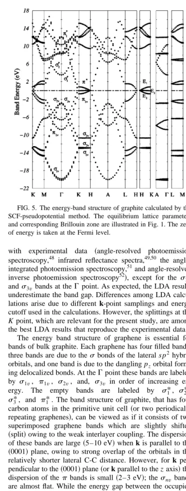
~with equilibrium structure! is shown in Fig. 5. It is in
gen-eral agreement with previous calculations that used norm-conserving,43,44 soft-transferable,33 and ultrasoft31 pseudopotentials, and also full-potential all-electron calcula-tions with a linearized augmented plane wave,45 linear muffin-tin orbitals,46 and a linear combination of Gaussian orbitals.47 The band energies are also in good agreement
with experimental data ~angle-resolved photoemission spectroscopy,48 infrared reflectance spectra,49,50 the angle-integrated photoemission spectroscopy,51and angle-resolved inverse photoemission spectroscopy52!, except for the s2v
ands3v bands at theG point. As expected, the LDA results underestimate the band gap. Differences among LDA calcu-lations arise due to different k-point samplings and energy cutoff used in the calculations. However, the splittings at the K point, which are relevant for the present study, are among the best LDA results that reproduce the experimental data.
The energy band structure of graphene is essential for bands of bulk graphite. Each graphene has four filled bands; three bands are due to thes bonds of the lateral s p2 hybrid orbitals, and one band is due to the dangling pzorbital
form-ing delocalized bonds. At theG point these bands are labeled by s1v, p1v, s2v, and, s3v in order of increasing
en-ergy. The empty bands are labeled by s1*, s2*,
s3*, and p1*. The band structure of graphite, that has four carbon atoms in the primitive unit cell ~or two periodically repeating graphenes!, can be viewed as if it consists of two superimposed graphene bands which are slightly shifted
~split! owing to the weak interlayer coupling. The dispersion
of these bands are large ~5–10 eV! when k is parallel to the
~0001! plane, owing to strong overlap of the orbitals in the
relatively shorter lateral C-C distance. However, for k per-pendicular to the~0001! plane ~or k parallel to the z axis! the dispersion of the p bands is small ~2–3 eV!; thesnv bands
are almost flat. While the energy gap between the occupied and unoccupied bands is ;6 eV at the G point, it dimin-ishes at the K point and along the KH direction where the bonding and antibonding bands join. Accordingly, graphite is a semimetal. Along the KH direction p bands originating from the bonding and antibonding combination of the pz
FIG. 4. Variation of the tip-surface separation~calculated at the close proximity of the tip! with the tip displacement.
FIG. 5. The energy-band structure of graphite calculated by the SCF-pseudopotential method. The equilibrium lattice parameters and corresponding Brillouin zone are illustrated in Fig. 1. The zero of energy is taken at the Fermi level.
orbitals located at a anda
8
atoms~i.e, pa and pa*) have significant dispersion due to their coupling along the z direc-tion, whereas the dispersion of the pb andpb* bands along the KH direction is rather small.The behavior of the p bands along the KH direction where they cross the Fermi level determines the Fermi sur-face, and hence is essential for various physical properties of the bulk graphite. The Fermi surface is generated by a k•p extension of these bands around the HKH axis~which is also known as the SWMc parametrization53!, or by their Fourier expansion54of the LDA bands. It includes six majority elec-tron pockets located around the H points, and 18 small pock-ets of minority electrons. The majority carrier concentrations ne.2.631018 cm23 and nh.2.231018 cm23 are reported
from various Shubnikov–de Haas and de Haas–van Alphen experiments measuring the period of the magnetoresistance and magnetic susceptibility.30 The experimental values are reproduced by the LDA bands.
The effect of the uniaxial strain on the electronic structure can be explained by a simple tight-binding picture. Consid-ering only pz orbitals in the primitive unit cell located at a, b, a
8
, andb8
atoms~see Fig. 1!,a anda8
atoms have significant overlap, whereas the overlap between b andb8
atoms is rather small. Consequently, the pa andpa* bands have to be dispersive, while the pb and pb* bands stay al-most flat along the KH direction. Furthermore, the dispersion of the pa and pa* bands along the KH direction increases with uniaxial compression, since the overlap betweenpaandpa*atoms increases. The modification of the electronic
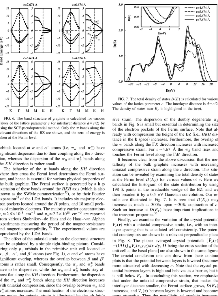
struc-ture under the uniaxial strain is illustrated by the ab initio bands shown in Fig. 6. In comply with the above arguments, the pa andpa* bands are strongly affected by the
compres-sive strain. The dispersion of the doubly degenerate pb bands in Fig. 6 is small but essential in determining the size of the electron pockets of the Fermi surface. Note that al-ready with compression the height of the BZ~i.e., HKH dis-tance in the k space! increases. Furthermore, the overlap of thep bands along theGK direction increases with increased compressive strain. For c;4.67 Å the pb band rises and touches the Fermi level along the GM direction.
It becomes clear from the above discussion that the me-tallicity of the bulk graphite increases with increasing uniaxial compressive strain along the z direction. This situ-ation can be revealed by examining the total density of states at the Fermi level D(EF) for various values of c. Here we
calculated the histogram of the state distribution by using 198 k points in the irreducible wedge of the BZ, and we then broaden it by a 0.5 eV Gaussian convolution. Our re-sults are illustrated in Fig. 7. It is seen that D(EF) may increase as much as 300% upon ;30% contraction of c. Such an increase at D(EF) have important implications in the transport properties.55
Finally, we examine the variation of the crystal potential Vc(r) with a uniaxial compressive strain, i.e., with an
inter-layer spacing that is calculated self-consistently. The poten-tial counterplots are shown in a relevant perpendicular plane in Fig. 8. The planar averaged crystal potentials @V¯c(z)
5(1/V)*VVc(x, y ,z)dx dy , V being the cross section of the
unit cell at the basal plane# are also shown in the same figure. The crucial conclusion one can draw from these contour plots is that the potential between layers is lowered~becomes more attractive! with decreasing c. Note that the crystal po-tential between layers is high and behaves as a barrier, but it is still below EF. In concluding this section, we emphasize
that under the uniaxial compressive strain, that makes the interlayer distance smaller, the Fermi surface grows, D(EF) increases, and Vc(r) between layers is lowered and becomes
more attractive. Thus the metallicity of graphite increases. Because of the low carrier concentration and weak screening, such effects are expected to survive at the contact region. FIG. 6. The band structure of graphite is calculated for various
values of the lattice parameter c ~or interlayer distance d5c/2) by using the SCF-pseudopotential method. Only thep bands along the relevant directions of the BZ are shown, and the zero of energy is taken at the Fermi level.
FIG. 7. The total density of states D(E) is calculated for various values of the lattice parameter c. The interlayer distance is d5c/2. The density of states near EFis highlighted in the inset.
IV. CONDUCTANCE THROUGH AN ATOMIC-SIZE CONTACT
In the electron transport between the STM tip and sample one normally distinguishes two regimes, i.e., tunneling and ballistic. The topological mode of STM ~in which the sepa-ration is large enough to allow a vacuum barrierF, and the bias voltage VB is small! operates in the tunneling regime. Since the tunneling conductance is proportional to the local density of states of the sample at the center of the tip and at the Fermi energy, r(EF,Rt),56 the tunneling current has
been rather small in STM measurements on the graphite sur-face. A significant value for the conductance can be achieved only at a small tip-sample separation, where the electronic contact is already established. Earlier, it was found that, due to the tip-sample interaction, F collapses6 for h;3.5 Å, and valence bands ~normally below EF) begin to overlap
with the Fermi level in regions different from the KH direc-tion of the BZ.8 Based on ab initio electronic structure cal-culations, it was also shown that the tip-induced states
~TILS! ~Ref. 6! form at the close proximity of the tip.
Actu-ally, TILS are nothing but the states that are confined in the constriction and are precursors to the current transporting states. In the present work, it is also shown that under the
uniaxial stress ~which is induced by the tip! the valence bands, which are normally below EF, begin to cross the
Fermi level. The Fermi-level crossing may induce sudden changes in physical properties, in particular in the tunneling conduction.57 Soler et al.5 were able to obtain only G
50.05(2e2/h) when the largest corrugation of line scans were achieved. The significant tip-induced deformation sug-gests that the barrier collapses at the contact. That the maxi-mum conductance measured is much smaller than 2e2/h dis-regards the opening of the first ballistic channel. Such a situation, in which the ballistic conductance cannot set in despite the collapse of the barrier, i.e.,F,EF, was pointed
out earlier.58 The effective barrier Feff, which may be greater than EF due to the size of the constriction, hinders
the ballistic transport.58On the other hand, it was argued that the flake of a dirt between the apex of the tip and the graphite surface increases the resistance and amplifies the corrugation.9 Nevertheless, apart from the spreading resis-tance, the conductance of a contact created by the sharp tip is generally smaller than 2e2/h. This is due to the small den-sity of states D(E), available at EF, since the current I }*EF
EF1eVB
Dt(E)D(E1eVB)T(E)dE. In this expression Dt
is the density of states of the tip, and T(E) is the transmis-sion coefficient. The crystal potential between graphenes is also rather shallow, only ;2 eV below EF. This may
pre-vent a current transporting state~or a ballistic channel! from forming at the contact between two electrodes. As a result the transmission coefficient T(E) becomes small. Another important feature that was not taken into account extensively in earlier works investigating the ballistic electron transport between two free-electron systems through a constriction is the actual topology of the Fermi surfaces. While the Fermi surface of a metal tip can be taken ~but not always! as a sphere, the Fermi surface of graphite is far from being simi-lar to a sphere. Since the narrow Fermi surface occurs at the corners of the hexagonal BZ, electrons at EF have a very
large lateral momentum\kK. Even if the lateral momentum
of the incoming electron cannot be conserved at the entrance of the contact, it should gain\kKafter it passed to the
graph-ite, which can be supplied by the acoustic phonons. There-fore, the matching of the Fermi surfaces of the electrodes at both sides of the contact is important; the conductance mea-sured at a low phonon population ~or at low temperature! is expected to reveal interesting features.
Here we first present a qualitative discussion of the con-ductance through a contact created by a sharp tip. As de-scribed in Sec. II, at a separation hs the surface layer of
graphite is first attracted and jumps to the contact. After this stage the separation between the tip and surface remain ap-proximately unchanged for a significant displacement of the tip, unless a plastic deformation sets in~see Fig. 4!. Accord-ingly the current under constant VB does not increases
sig-nificantly. As s increases, the tip presses the underlying graphite surface, as shown in Fig. 3. This decreases inter-layer distance, lowers the interinter-layer potential and increases the density of states at EF~see Figs. 6–8!. Even if T(E) ~that also increases with s) is assumed to be unchanged, the cur-rent and hence G increase continuously with s in the elastic region. However, as seen in Fig. 3, at certain range of s
~where G reaches its highest value! the compressive stress
FIG. 8. Contour plots of the crystal potential on a perpendicular plane and the plane-averaged crystal potential V¯c(z) as a function
of c. The contour interval is 1.5 eV in each graph, and the indi-cated contour values are the maximum values with respect to the Fermi level.
exceeds a threshold value whereby the tip punctures the first layer by atomic rearrangements or by creating flakes at its close proximity. This relaxes the strain in the layers. As a result, the interlayer distance and the density of states are retrieved. Since the tip faces now the second layer but with a larger separation, the conductance G decreases suddenly. As the tip first presses than punctures the graphite layers sequen-tially with increasing s, the conductance first increases from a low level to a high level and then falls again to a low level. Due to the electron transport from the sides of the tip to the already punctured layers, the low level value of G may in-crease with an increasing number of layers. Nevertheless, G(s) is expected to vary between low and high conductance values. This situation may be different if a blunt ~and flat! metal tip presses the graphite surface and forms a contact with large Ac. Whether the quantum ballistic transport
oc-curs for large contact area depends on the matching of the Fermi surfaces.
We now quantify the above discussion about G(s) by calculating the conductance of the contact described in Fig. 9. Two metal tips ~Al oriented along the @111# direction! with a single atom at the apex make point contact from both surfaces of the graphite ~0001! plane. This contact can be described by a tapered constriction that has cylindrical sym-metry and is connected to the free-electron systems from both sides. The Al electrodes are taken as free-electron sys-tems with an electron density and EF appropriate for Al. The
radius of the constriction through the graphite is determined from our earlier ab initio calculation dealing with Al tip and graphite surface8and present calculations. The crystal poten-tial Vc(r) of graphite between two adjacent layers raises to ;2 eV below EF. This creates a saddle-point effect.6,59The
potential of the constriction is described in Fig. 9~a!. After the mechanical contact is established, the displacement of the tip decreases the interlayer distance c/2 locally by applying a uniaxial compression. This, in turn, induces changes in the electronic structure and the crystal potential. For example, for the displacement s;0.4 Å ~where the puncture sets in!, the saddle-point potential is lowered by 1.8 eV for a three-layer slab shown in Fig. 9~a!. In this simple constriction model, where the electrodes are represented by a free-electron gas system, we can consider only the variation of graphite potential and the radius of the constriction, i.e., Vc(s) and rc(s). Therefore, the calculation of conductance
with Vc(s) and rc(s) is expected to describe the essential
features of the G(s) curve.
To calculate conductivity, we used the recursion transfer-matrix method proposed by Hirose and Tsukada;60and it was applied in similar types of calculations in Ref. 61. In this approach, we replace our constriction shown in Fig. 9~a! by a periodically repeating supercell structure (60360 a.u.2) in the x y plane defining the contact. This allows us to express the jth scattering state in terms of Laue expansion:
Cj~r!5eikzz•rzz
(
l cl j~z!e
iGuul•rzz. ~2!
Here kuuand Guucorrespond to the wave vector in the BZ and the reciprocal-lattice vector of the supercell in the xy plane, respectively. The summation over Guuis truncated, and a
cut-off energy of 30 eV was sufficient for convergence. Deep in the Al structure, the wave functionCj(r) can be expressed
as Cj~r!5
(
i ti jH
e ikziz e2kz izJ
e i~ki1Gii!•ri ~z>z R!, Cj~r!5eikz j •zei~ki1Gij!•ri1(
i ri jH
e2ikz i •z ekz i •zJ
e i~ki1Gii!•ri ~z<zL!, ~3!where zR and zL are the boundaries of the constriction. ti j and ri j are transmission and reflection coefficients,
corre-sponding to states kzi and kzj, and they are determined by using transfer-matrix method. We note that in this approach, FIG. 9. ~a! A constriction model describing the point contact created by two Al~111! tip on both sides of a thin graphite slab. The variation of the potential relative to the vacuum level is shown below. The potential has a cylindrical symmetry.~b! Variation of the conductance with the displacement of the tip. The dotted and dashed curves correspond to cases~i! and ~ii! explained in the text, respectively.fvis the work function, and rc, Dc, zR, and zLare
defined in the text.
the potential should be smooth and the constriction is divided into ‘‘small strips’’ along the propagation direction ~for re-cursive purposes!, otherwise results diverge. To smooth out the potential at both ends of Al tips, we used a Fermi func-tion of width 3 a.u., and a discretizafunc-tion width of 0.1 a.u. was applied to obtain convergent results. In our model, we assume that Vc(s) varies linearly (9.3 eV→7.54 eV) as a
function of s. Furthermore the mean width of the saddle-point potentialDc also decreases linearly with s. The radius
of the constriction, rc(s), is also a difficult parameter to
determine. Here we assume that rc(s) is uniform between
the Al tips, and consider two limiting cases: ~i! rc(s)5r0
52.2 Å, i.e., the value corresponding to hs;2 Å at the
electronic contact,7 ~ii! rc(s)5r011.23s, allowing a 50% expansion of contact area before puncture occurs. Further-more, linear-response theory is assumed, and we obtain:
G52e 2 h
(
i j uTi ju 252e 2 h(
i j ~di j2uRi ju 2!, ~4!where i and j run over all conducting states, Ti j 5ti j3(kz i/k z j)1/2, and R i j5ri j3(kz i/k z j)1/2. We have consid-ered only the case where kuu50, since the supercell area of the boundary condition is large and and hence the area of the supercell BZ is negligible. We have applied both formulas in Eq.~4! for determining G, because they serve as a good test of whether the results have converged. The calculated G(s) curves are shown in Fig. 9~b!. As argued above, G(s) in-creases with increasing s until a plastic deformation ~or puncturing of the graphene! sets in. Once the graphene is punctured by the sharp tip, the conductance decreases
sud-denly. For a sharp tip having a single atom at the apex, the radius of the constriction is normally small. In Fig. 9~b!, G attains a value smaller than 2e2/h, corresponding to case~i! with rc5r0. For case~ii!, where rc(s) is allowed to expand,
a ballistic channel is opened before the puncturing. We also note thatDG/Ds of actual graphite is expected to be much smaller than that of Fig. 8~c!, since the same level of com-pressive strain in Fig. 8~c! requires much larger s in the multilayer graphite. For the constriction described in Fig. 9~a!, s.Dc.
V. CONCLUSIONS
In this work, based on the atomistic simulation of the contact and ab initio electronic structure calculations of graphite under uniaxial compressive strain we showed the following:~i! The graphenes are punctured sequentially by a sharp tip pressing the surface. ~ii! The tip-induced elastic deformation between two consecutive puncture increases the density of states at the close proximity of the tip, and lowers the crystal potential: Hence, the metallicity of graphite in-creases with uniaxial compressive strain of basal planes.~iii! Accordingly the conductance between two consecutive punc-ture increases, but falls suddenly upon the onset of a new puncture. This is a behavior different from the usual metal contacts.
ACKNOWLEDGMENT
We thank K. Nordlund for providing his empirical poten-tial data.
1G. Binning, H. Fuchs, Ch. Gerber, H. Rohrer, E. Stoll, and E.
Tosatti, Europhys. Lett. 1, 31~1985!.
2A. Selloni, P. Carnevali, E. Tosatti, and C. D. Chen, Phys. Rev. B 31, 2602~1985!.
3I. P. Batra, N. Garcia, H. Rohrer, H. Salemink, E. Stoll, and S.
Ciraci, Surf. Sci. 181, 126~1987!.
4D. Toma´nek, S. G. Louie, D. J. Mamin, D. W. Abraham, R. E.
Thompson, E. Ganz, and J. Clarke, Phys. Rev. B 35, 7790 ~1987!; D. Toma´nek and S. G. Louie, ibid. 37, 8327 ~1988!.
5J. M. Soler, A. M. Baro, N. Garcia, and H. Rohrer, Phys. Rev.
Lett. 57, 444~1986!.
6S. Ciraci and I. P. Batra, Phys. Rev. B 36, 6194~1987!; E.
Tek-man and S. Ciraci, Phys. Scr. 38, 486~1988!; Phys. Rev. B 40, 10 286~1989!.
7S. Ciraci, in Basic Concepts and Applications of Scanning
Tun-neling Microscopy and Related Techniques, edited by H. Ro-hrer, N. Garcia, and J. Behm ~Kluwer, Amsterdam, 1989!, p. 119.
8S. Ciraci, A. Baratoff, and I. P. Batra, Phys. Rev. B 41, 2763
~1990!.
9J. B. Pethica, Phys. Rev. Lett. 57, 3235~1986!; H. J. Mamin, E.
Ganz, D. W. Abraham, R. E. Thomson, and J. Clarke, Phys. Rev. B 34, 9015~1986!.
10A. Oral~unpublished!.
11J. K. Gimzewski and R. Mo¨ller, Phys. Rev. B 36, 1284~1987!. 12N. D. Lang, Phys. Rev. B 36, 8173~1987!.
13J. Ferrer, A. Martı´n-Rodero, and F. Flores, Phys. Rev. B 38, 10
113~1988!.
14S. Ciraci and E. Tekman, Phys. Rev. B 40, 11 969 ~1989!; E.
Tekman and S. Ciraci, ibid. 43, 7145~1991!.
15N. Agraı¨t, G. Rubio, and S. Vieria, Phys. Rev. Lett. 74, 3995
~1995!; G. Rubio, N. Agraı¨t, and S. Vieria, ibid. 76, 2302 ~1996!.
16A. Stalder and U. Du¨rig, Appl. Phys. Lett. 68, 637~1996!. 17A. P. Sutton and J. B. Pethica, J. Phys.: Condens. Matter 2, 5317
~1990!.
18T. N. Todorov and A. P. Sutton, Phys. Rev. Lett. 70, 2138~1993!. 19A. Buldum, S. Ciraci, and I. P. Batra, Phys. Rev. B 57, 2468
~1998!.
20H. Mehrez and S. Ciraci, Phys. Rev. B 56, 12 632~1997!; H.
Mehrez, S. Ciraci, C. Y. Fong, and S. Erkoc, J. Phys. Condens. Matter 9, 10 843~1997!.
21
For recent experiments and theoretical works see Refs. 18 and 20, and also N. Agraı¨t, J. G. Rodrigo, and S. Vieira, Phys. Rev. B
47, 12 345~1993!; J. I. Pascual et al., Phys. Rev. Lett. 71, 1852
~1993!; J. I. Pascual et al., Science 267, 1793 ~1995!; J. M. Krans, C. J. Muller, I. K. Yanson, Th. C. M. Govaert, R. Hesper, and J. M. van Ruitenbeek, Phys. Rev. B 48, 14 721~1993!; J. M. Kranz, C. J. Muller, N. van der Post, F. R. Postma, A. P. Sutton, T. N. Todorov, and J. M. van Ruitenbeek, Phys. Rev. Lett. 74, 2146~1995!; L. Olesen, E. Laegsgaart, I. Stensgaard, F. Besen-bacher, J. Schio”tz, P. Stoltze, K. W. Jacobsen, and J. K.
No”rskov, ibid. 72, 2251 ~1994!; 74, 2147 ~1995!.
22Yu V. Sharvin, Zh. E´ ksp. Teor. Fiz. 48, 984 ~1965! @Sov. Phys.
JETP 21, 655~1965!#.
23
K. Hansen, E. Laegsgaard, I. Stenggaard, and F. Besenbacher, Phys. Rev. B 56, 2208~1997!.
24H. Mehrez and S. Ciraci, Phys. Rev. B~to be published!. 25C¸ . Kılıc¸, M.S. thesis, Bilkent University, 1997.
26K. Nordlund, J. Keinonen, and T. Mattila, Phys. Rev. Lett. 77,
699~1996!.
27J. Tersoff, Phys. Rev. Lett. 56, 632 ~1986!; 61, 2879 ~1988!;
Phys. Rev. B 37, 6991~1988!.
28Y. Baskin and L. Mayer, Phys. Rev. 100, 544~1955!.
29D. Sands, Introduction to Crystallography~Benjamin-Cummings,
Reading, MA, 1969!.
30N. B. Brandt, S. M. Chudinov, and Ya. G. Ponomarev,
Semimet-als~Elsevier, Amsterdam, 1988!.
31J. Furthmu¨ller, J. Hafner, and G. Kreese, Phys. Rev. B 50, 15 606
~1994!.
32L. A. Girifalco and R. A. Ladd, J. Chem. Phys. 25, 693~1956!. 33M. C. Schabel and J. L. Martins, Phys. Rev. B 46, 7185~1992!. 34J. H. Rose, J. Ferrante, and J. R. Smith, Phys. Rev. Lett. 47, 675
~1981!; J. H. Rose, J. R. Smith, and J. Ferrante, Phys. Rev. B 28, 1835~1983!.
35G. C. Abell, Phys. Rev. B 31, 6184~1985!.
36D. P. DiVincenzo, E. J. Mele, and N. A. W. Holzwarth, Phys.
Rev. B 27, 2458~1983!.
37M. T. Yin and M. L. Cohen, Phys. Rev. Lett. 50, 2006~1983!;
Phys. Rev. B 29, 6996~1984!.
38M. P. Allen and D. J. Tildesley, Computer Simulation of Liquids
~Oxford University Press, New York, 1987!.
39The puncture of the first layer of graphite was pointed out first by
F. F. Abraham and I. P. Batra, Surf. Sci. 209, L125 ~1989!, where a single atom was pressed. Present results indicate se-quential puncture by a realistic tip.
40D. M. Ceperley and B. J. Alder, Phys. Rev. Lett. 45, 566~1980!. 41G. B. Bachelet, D. R. Hamann, and M. Schlu¨ter, Phys. Rev. B 26,
4199~1982!.
42W. Kohn and P. Vashishta, in Theory of the Inhomogeneous
Elec-tron Gas, edited by S. Lundqvist and N. H. March ~Plenum, New York, 1983!.
43J.-C. Charlier, X. Gonze, and J.-P. Michenaud, Phys. Rev. B 43,
4579~1991!; Europhys. Lett. 28, 403 ~1994!.
44N. A. W. Holzwarth, S. G. Louie, and S. Rabii, Phys. Rev. B 26,
5382~1982!.
45
H. J. F. Jansen and A. J. Freeman, Phys. Rev. B 35, 8207~1987!.
46R. Ahuja, S. Auluck, J. Trygg, J. M. Wills, O. Eriksson, and B.
Johansson, Phys. Rev. B 51, 4813~1995!.
47J. C. Boettger, Phys. Rev. B 55, 11 202~1997!.
48W. Eberhardt, L. T. McGovern, E. W. Plummer, and J. E.
Fis-cher, Phys. Rev. Lett. 44, 200~1980!; A. R. Law, J. J. Barry, and H. P. Hughes, Phys. Rev. B 28, 5332~1983!; D. Marchand, C. Fretigny, M. Lagues, F. Batallan, C. Simon, I. Rosenman, and R. Pinchaux, ibid. 30, 4788~1984!; T. Takayashi, H. Tokailin, and T. Sawaga, Solid State Commun. 52, 765~1984!.
49M. Hanfland, K. Syassen, and R. Sonnenschein, Phys. Rev. B 39,
12 598~1989!.
50G. Bellodi, A. Borghesi, G. Guizzetti, L. Nosenzo, E. Reguzzoni,
and G. Samoggia, Phys. Rev. B 12, 5951~1975!.
51
A. Bianconi, S. B. M. Hagstro¨m, and R. Z. Bachrach, Phys. Rev. B 16, 5543~1977!.
52Th. Fauster, F. J. Himpsel, J. E. Fischer, and E. W. Plummer,
Phys. Rev. Lett. 51, 430~1983!; I. Scha¨fer, M. Schlu¨lter, and M. Skibowski, Phys. Rev. B 35, 7663 ~1987!; F. Maeda, T. Taka-hashi, H. Ohsawa, S. Suzuki, and H. Suematsu, ibid. 37, 4482 ~1988!; R. Claessen, H. Cartensen, and M. Skibowski, ibid. 38, 12 582~1988!; I. R. Colins, P. T. Andrews, and A. R. Law, ibid.
38, 13 348~1988!.
53J. C. Slonczewski and P. R. Weiss, Phys. Rev. 109, 272~1958!; J.
W. McClure, ibid. 108, 612~1957!.
54L. G. Johnson and G. Dresselhaus, Phys. Rev. B 7, 2275~1973!. 55H. Mehrez, S. Ciraci, A. Buldum, and I. P. Batra, Phys. Rev. B
55, R1981~1997!.
56J. Tersoff and D. R. Hamann, Phys. Rev. Lett. 50, 1998~1983!;
Phys. Rev. B 31, 805~1985!.
57O. J. Marti, Ph.D. thesis, Eidgeno¨ssische Technische Hochschule,
Zu¨rich, 1986.
58S. Ciraci, A. Baratoff, and I. P. Batra, Phys. Rev. B 42, 7618
~1990!.
59M. Bu¨ttiker, Phys. Rev. B 41, 7906~1990!.
60K. Hirose and M. Tsukada, Phys. Rev. B 51, 5278~1995!. 61M. Brandbyge, K. W. Jacobsen, and J. K. No
”rskov, Phys. Rev. B
55, 2637~1997!.