Research Article
Mosaic Structure Characterization of the AlInN Layer
Grown on Sapphire Substrate
Engin Arslan,
1Pakize Demirel,
1Huseyin Çakmak,
1Mustafa K. Öztürk,
2and Ekmel Ozbay
1,31Nanotechnology Research Center (NANOTAM), Department of Physics, Bilkent University, 06800 Ankara, Turkey 2Department of Physics, Faculty of Science and Arts, Gazi University, Teknikokullar, 06500 Ankara, Turkey 3Department of Electrical and Electronics Engineering, Bilkent University, 06800 Ankara, Turkey
Correspondence should be addressed to Engin Arslan; [email protected]
Received 24 March 2014; Revised 6 June 2014; Accepted 9 June 2014; Published 10 August 2014 Academic Editor: Xinhe Zheng
Copyright © 2014 Engin Arslan et al. This is an open access article distributed under the Creative Commons Attribution License, which permits unrestricted use, distribution, and reproduction in any medium, provided the original work is properly cited. The 150 nm thick, (0001) orientated wurtzite-phase Al1−xInxN epitaxial layers were grown by metal organic chemical vapor deposition on GaN (2.3𝜇m) template/(0001) sapphire substrate. The indium (x) concentration of the Al1−xInxN epitaxial layers was changed as 0.04, 0.18, 0.20, 0.47, and 0.48. The Indium content (x), lattice parameters, and strain values in the AlInN layers were calculated from the reciprocal lattice mapping around symmetric (0002) and asymmetric (10–15) reflection of the AlInN and GaN layers. The mosaic structure characteristics of the AlInN layers, such as lateral and vertical coherence lengths, tilt and twist angle, heterogeneous strain, and dislocation densities (edge and screw type dislocations) of the AlInN epilayers, were investigated by using high-resolution X-ray diffraction measurements and with a combination of Williamson-Hall plot and the fitting of twist angles.
1. Introduction
Because of the large band gap, large breakdown field, and strong spontaneous and piezoelectric polarization field’s properties of the III-nitride materials systems, they have been used in optoelectronic devices, such as light emitting diodes, blue/ultraviolet lasers, metal-semiconductor field effect transistors, modulation-doped field effect transistors, photodetectors, and high temperature/high power electronic devices [1–3]. The structural quality of GaN based alloys can significantly affect its electrical and optical properties and also the performance of devices [1–7]. One of the most common problems for the growth of group GaN based alloys heterostructures is the lattice constant mismatch between the binary and ternary compounds of Ga, In, Al, and N elements [1–4,7–9]. The mismatches in multilayered struc-tures result in strain and potentially crack formation that deteriorates the performance of devices [7, 10, 11]. Many studies have been performed to improve the structural quality of GaN based alloys and the performance of devices, such
as increasing the Al composition of an AlGaN barrier, using a thin AlN spacer layer at the AlGaN/GaN interface, and replacing the GaN by InGaN as the channel and AlGaN by AlInN layer as a barrier [12, 13]. Among these studies, it is possible to grow a lattice-matched AlInN layer on GaN layer for an In concentration of∼18% [12–14]. Due to its promising electronic properties, polarization effects, and high thermal stability, the lattice-matched AlInN material system has become of interest for electronic applications [15–
17]. The lattice-matched AlInN barrier in the AlInN/GaN high electron mobility transistor (HEMTs) shows superior performance compared to the AlGaN/GaN HEMTs [12,
13]. In addition, the use of appropriate AlInN enables the fabrication of lattice-matched GaN-based heterostructures that can be used for high-performance laser diodes [17]. Furthermore, AlInN alloys can possibly be used for light emitters and detectors operating in extremely wide spectral regions covering from deep infrared to UV since the alloys band-gap energy(𝐸𝑔) can range from 0.7 eV (InN) to 6.2 eV (AlN) [1–3].
Volume 2014, Article ID 980639, 11 pages http://dx.doi.org/10.1155/2014/980639
Despite the many advantages for devices, the growth of AlInN alloys over the full compositional range is extremely difficult due to the large differences in the chemical and phys-ical parameters between AlN and InN. Due to the different growth conditions of AlN and InN and the expected large immiscibility gap of the ternary alloy, the growth of AlInN in the whole compositional range is challenging [18–20].
The GaN based structures are usually grown on highly lattice-mismatched substrates, such as sapphire, SiC, or Si [4,11]. The large lattice mismatch and large difference in the thermal expansion coefficients between the GaN layer and the substrates (sapphire, SiC, and Si) cause a high level of in-plane stress and threading dislocation generation in the epitaxial layers and reduce the crystal quality of the GaN layers during the growth [4,5,8–11]. The high level of in-plane stress and threading dislocation in the epitaxial layers affect the performance reliability of the device [1–5,10]. The dis-torted GaN based semiconductor material can be described with mosaic structures that can be characterized by means of vertical and lateral coherence lengths (average size of the mosaic blocks) twist and tilt angle, heterogeneous strain, and dislocation densities (edge and screw type threading dislocations) [8, 9,21–31]. The tilt describes the rotation of the mosaic blocks out of the growth plane and the twist in their in-plane rotation. The average absolute values of the tilt and twist are directly related with the full width at half maximum (FWHM) of the corresponding distributions of the crystallographic orientations [21,23–31].
In this study, we present investigations of the mosaic properties of Al1−𝑥In𝑥N grown in the composition range 0.04, 0.18, 0.20, 0.47, and 0.48 on GaN/sapphire structures by metal organic chemical vapor phase deposition (MOCVD). The main aim of the work is to grow AlInN layers on a GaN template with a wide range of indium content and investi-gate the mosaic structure parameters of the AlInN layers. The mosaic structure features (such as lateral and vertical coherence lengths, tilt and twist angle, and heterogeneous strain) and dislocation densities (edge and screw type dislo-cations) of hexagonal AlInN layers were determined by HR-XRD measurements. Additionally, atomic force microscopy (AFM) imaging was performed in order to obtain detailed knowledge on the surface morphology of the samples.
2. Experimental Procedure
Epitaxial Al1−𝑥In𝑥N (𝑥 = 0.04, 0.18, 0.20, 0.47, and 0.48) layers were grown on double-polished 2-inch diameter sap-phire(Al2O3) substrates in a low pressure MOCVD reactor (Aixtron 200/4 HT-S) by using trimethylgallium (TMGa), trimethylaluminum (TMAl), trimethylindium (TMIn), and ammonia as Ga, Al, In, and N precursors, respectively. Before the epitaxial growth, the Al2O3 substrate was annealed at 1110∘C for 15 min in order to remove surface contamination. The buffer structures of all the samples consisted of a 15 nm thick, low-temperature (710∘C) GaN nucleation layer, and high temperature (1100∘C) 2.3𝜇m GaN template layer. After GaN template layer growth, a nominally 150 nm undoped AlInN layer was grown. In this study, five different samples were grown, with a different indium concentration, on GaN
AlInN layer150 nm
GaN template layer2.3 𝜇m
GaN nucleation layer15 nm
Al2O3substrate
Figure 1: Schematic drawing of the AlInN/GaN/Al2O3structures.
template layers (Figure 1). The In content was changed by changing the growth temperature and TMIn/(TEGa+TMIn) ratio. The growth temperatures and the TMIn/(TEGa+TMIn) ratio of the samples are 900, 830, 830, 730, and 745∘C and 0.69, 0.69, 0.43, 0.75, and 0.75 for an indium content (𝑥) of 0.04, 0.18, 0.20, 0.47, and 0.48, respectively. The samples were identified with consideration of the indium content as samples A, B, C, D, and E, 0.04, 0.18, 0.20, 0.47, and 0.48, respectively.
The crystalline quality of the GaN layers was examined by high resolution X-ray diffraction (HR-XRD). The X-ray diffraction was performed using a Rigaku SmartLab high-resolution diffractometer system, delivering CuK𝛼1 (1.544 ˚A) radiation, and 4-bounce Ge(220) symmetric monochroma-tor. Data were collected on the symmetric (0002), (0004), and (0006) and asymmetric (10–15), (12–31), and (10–12) reflections as reciprocal space mappings (RSMs) or just𝜔 − 2𝜃 scans. Doubled-axis rocking curves of the (10–15), (12– 31), and (10–12) in𝜔-scans and Φ-scans were recorded in skew diffraction geometry (𝜔 = 𝜃). The samples surface morphology was characterized by atomic force microscopy (AFM) in contact mode with a commercial VEECO CPII.
3. Results and Discussion
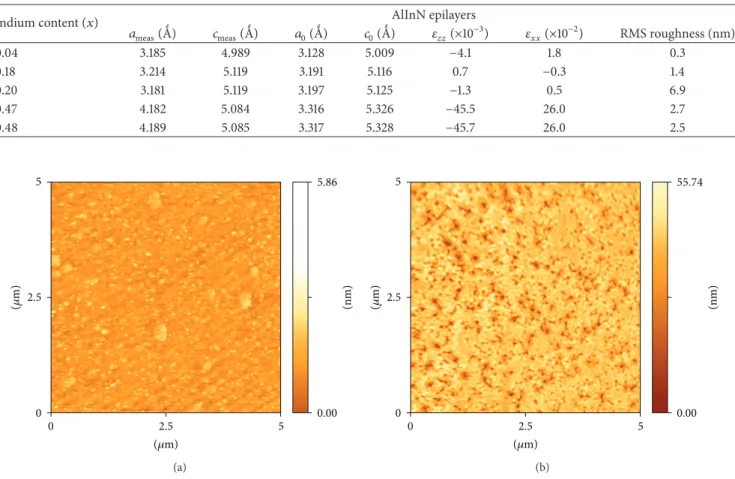
The surface morphology of the AlInN epilayers grown on GaN template layers is characterized by AFM. Figures2(a)
and 2(b) show the AFM image of the samples A and C. The root-mean-square (RMS) roughness (5 × 5 𝜇m2 scan) varies between 0.3 nm (for sample A) and 6.9 nm (for sample C). Sample A has a smooth surface with low rms roughness (rms = 0.3 nm) compared to the other samples. The variation of the RMS roughness with indium content(𝑥) in an AlInN layer is shown in Table 1. Based on the observation from
Table 1, the RMS roughness values of the AlInN layers did not
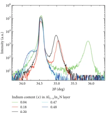
show any systematic dependence on the indium content. HR-XRD measurements were performed for all of the samples to investigate the crystal phase of the AlInN epilayer on GaN template layer.Figure 3shows the 2𝜃-𝜔-scan
HR-XRD pattern of (0002) peaks of the AlInN/GaN samples. The diffraction patterns exhibited the wurtzite AlInN epilayers
Table 1: The In content (𝑥), lattice parameters ameasand cmeasand the strain components𝜀𝑧𝑧and𝜀𝑥𝑥of the AlInN epilayers, calculated from the
RSM measurements and the relaxed lattice parameters𝑐0and𝑎0of the AlInN epilayers calculated by using Vegard’s law are given in column 4 and 5, respectively. In the last column, the RSM roughness of the5 × 5 nm2scan AFM image is demostrated (the uncertainty in𝑥 values is
approx.Δ𝑥 = ±0.00277).
Indium content (𝑥) AlInN epilayers
𝑎meas(>) 𝑐meas(>) 𝑎0(>) 𝑐0(>) 𝜀𝑧𝑧(×10−3) 𝜀𝑥𝑥(×10−2) RMS roughness (nm)
0.04 3.185 4.989 3.128 5.009 −4.1 1.8 0.3 0.18 3.214 5.119 3.191 5.116 0.7 −0.3 1.4 0.20 3.181 5.119 3.197 5.125 −1.3 0.5 6.9 0.47 4.182 5.084 3.316 5.326 −45.5 26.0 2.7 0.48 4.189 5.085 3.317 5.328 −45.7 26.0 2.5 0 2.5 5 0 2.5 5 (𝜇m) (𝜇 m) 5.86 0.00 (nm) (a) 0 2.5 5 0 2.5 5 (𝜇m) (𝜇 m) 55.74 0.00 (nm) (b)
Figure 2: AFM images (5× 5 𝜇m2scan) of AlInN layers in (a) sample A and (b) sample C.
with different indium concentration clearly observed at 35.91, 35.05, 34.99, 34.31, and 34.26∘ for samples A, B, C, D, and E, respectively. Also from Figure 3, the (0002) peaks of the wurtzite GaN template layers are seen at similar angle values. No peaks are identified except those corresponding to GaN template layers and InAlN epilayers. FromFigure 3, no reflections other than those corresponding to GaN and InAlN can be identified, these results indicating that we have grown homogeneous material without phase separation and metal segregation.
In order to investigate the in-plane alignment of an AlInN epilayer and GaN template layer, in which an in-plane Φ-scan was also taken by rotating the sample around its surface-normal direction, theΦ-scan patterns of the (10–15) plane of sample B are given inFigure 4. As can be seen inFigure 4, the diffraction peaks from the (10–15) plane of GaN and AlInN were observed at∼60∘ intervals, confirming the hexagonal structure of the AlInN epilayer and GaN template layer.
HR-XRD provides highly precise measurement on the lattice parameters of a thin film. The X-ray reciprocal space map (RSM) is a powerful tool for detailed structural charac-terization of imperfect crystalline layers [31,32]. The RSM is based on two-dimensional diffraction measurements in the
scattering plane: in the perpendicular direction (i.e., 2𝜃-𝜔-scan) and in the parallel direction along the diffraction vector (i.e.,𝜔-scan). Correspondingly, a map taken from asymmet-ric reflection of the samples allows one to deduce both the in-plane(𝑎) and the out-of-plane (𝑐) lattice parameters and thus to simultaneously determine the residual strain and stress as well as the exact alloy composition of the layers [31,32]. The lattice parameter𝑎 and 𝑐 can be determined by XRD directly from theℎ𝑘𝑙 reflections in the symmetric 𝜔-2𝜃 scan by combining Bragg’s equation 𝑑ℎ𝑘𝑙 = 𝑛𝜆/2 sin(𝜃), where (ℎ𝑘𝑙) is the Miller index in (ℎ𝑘 − (ℎ + 𝑘)𝑙) notation, 𝜆 is the wavelength of the X-rays, and𝜃 is the Bragg angle, with the expression for interplanar spacing in hexagonal structures given below [31,32]:
𝑑ℎ𝑘𝑙= 1
√(4/3) ((ℎ2+ 𝑘2+ ℎ𝑘) /𝑎2) + (𝑙2/𝑐2). (1) In order to calculate 𝑑ℎ𝑘𝑙 values by using (1) at least two reflections measurements are needed (because of two unknowns (𝑎 and 𝑐)). Generally, one or two high-angle symmetric reflections are measured from the (0004), and/or (0006) planes, from which𝑐 can be found directly [31]. On
In te n si ty (a.u .) 106 105 104 103 102 101 34.0 34.5 35.0 35.5 36.0 2𝜃 (deg) 0.04 0.18 0.20 0.47 0.48
Indium content (x) in Al1−xInxN layer
Figure 3: HR-XRD 2𝜃-𝜔 scans of the (0002) reflection of the AlInN/GaN/Al2O3samples.
the other hand, the 𝑎 values can be calculated just with one or two high-angle asymmetric reflections measurement (typically (10–15), (20–25), or (20–24) reflection). From high-angle asymmetric reflections𝑎 values can be determined by combining the value of𝑐 found previously [31].
The lattice and thermal mismatch between the substrate and III-nitrides disallow growth directly on substrates (for example SiC, Al2O3, and Si as a substrate). Growth on high mismatched substrates can result in dislocations leading to domain walls and highly mosaic films. In order to improve the crystalline quality of the III-nitrides layers different type of buffer structures (e.g., LT-AlN, LT-GaN, HT-GaN layer, etc.) needed to use between epilayers and substrates. The mosaic structures of the GaN growth on Si, SiC, and sapphire is strongly influenced by the growth conditions of the nucleation layer and is known to affect the electronic properties of thin films [8,9]. In most cases, a GaN layer is used as a buffer layer [4,11]. Between the group-III nitride alloy film and the GaN buffer, a nearly perfect in-plane ori-entation is established [8, 9]. In order to determine the strain and composition of the layer, commonly a peak from another III-nitride layer is used as the “substrate” [31]. If the material is assumed to be unstrained, then composition is the only factor affecting the lattice parameters and only lattice parameters need to be measured. For this case, Vegard’s law has been applied, which states that the lattice parameters of an alloy will vary linearly between the end members. For the unstrained𝑐0 and𝑎0lattice parameter of AlInN (where𝑥 is the mole fraction of InN), Vegard’s law is given by [8,9,31,33]
𝑐AlInN
0 = (1 − 𝑥) 𝑐0AlN− 𝑥𝑐0InN, 𝑎AlInN
0 = (1 − 𝑥) 𝑎0AlN− 𝑥𝑎InN0 .
(2)
If the strained lattice parameters𝑎 and 𝑐 are known, the sample strain can be taken into account in estimates of the composition: [𝑐AlInN− 𝑐0(𝑥)] 𝑐0(𝑥) = −] [𝑎AlInN− 𝑎0(𝑥)] 𝑎0(𝑥) , (3) ] = 2𝐶13(𝑥) 𝐶33(𝑥), (4)
where𝑐AlInNand𝑎AlInNare the measured lattice parameters (which take into account strain),𝑐0 and 𝑎0 are the relaxed parameters predicted by Vegard’s law, and𝐶13(𝑥) and 𝐶33(𝑥) are elastic constants linearly interpolated from the binary values.] is the Poisson’s ratio for a hexagonal crystal system biaxially strained perpendicular to[0001] and is given by (4). The linear relationship for the Poisson’s ratio as a first-order approximation is given by
]AlInN= (1 − 𝑥) ]AlN+ 𝑥]InN. (5)
Substitution of𝑎0AlInN, 𝑐0AlInN, and]IAlInNinto (3) obtained a cubic equation for𝑥 given below
𝐾𝑥3+ 𝐿𝑥2+ 𝑀𝑥2+ 𝑁 = 0. (6)
The coefficient (K, L, M, N) of (6) can be determined by a algebraic calculation. A more detailed𝑎, 𝑐, and ] dependent coefficient K, L, M, N expression can be found in [33]. The solution of (6) gives the In mole fraction 𝑥 in the case of Al1−𝑥In𝑥N. There are three real solutions, but only one physically meaningful value of𝑥 in the interval 0 ≤ 𝑥 ≤ 1. By using calculated mole fraction𝑥, in (2), and (5), the relaxed lattice parameters of the AlInN alloy film𝑎0AlInNand𝑐0AlInN, as well as Poisson’s ratio]AlInN, can be obtained. In order to perform the calculations, in addition to the measured lattice parameters, the relaxed lattice constants of the AlN (𝑎AlN
0 =
3.112 ˚A, 𝑐AlN
0 = 4.982,) [31,34] and the InN (𝑎0InN= 3.538 ˚A, 𝑐InN
0 = 5.703,) [31,34] and the elastic constant (𝐶13 = 108 and 𝐶33 = 396 GPa) for AlN and (𝐶13 = 92 and 𝐶33 = 223 GPa) InN [31,34] are used as input parameters. The in-plane and out-of-in-plane strain components can be defined as 𝜀𝑥𝑥= [𝑎meas−𝑎0]/𝑎0and𝜀𝑧𝑧= [𝑐meas−𝑐0]/𝑐0, where𝑎measand 𝑐measare the measured lattice parameters, while𝑎0and𝑐0are the relaxed parameters given by Vegard’s law [31,33].
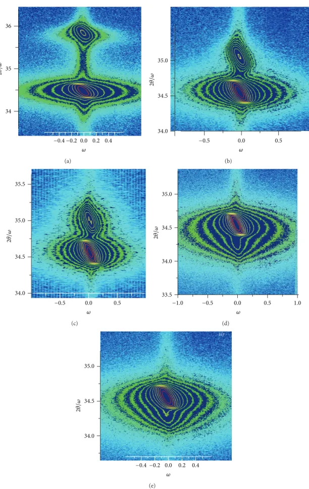
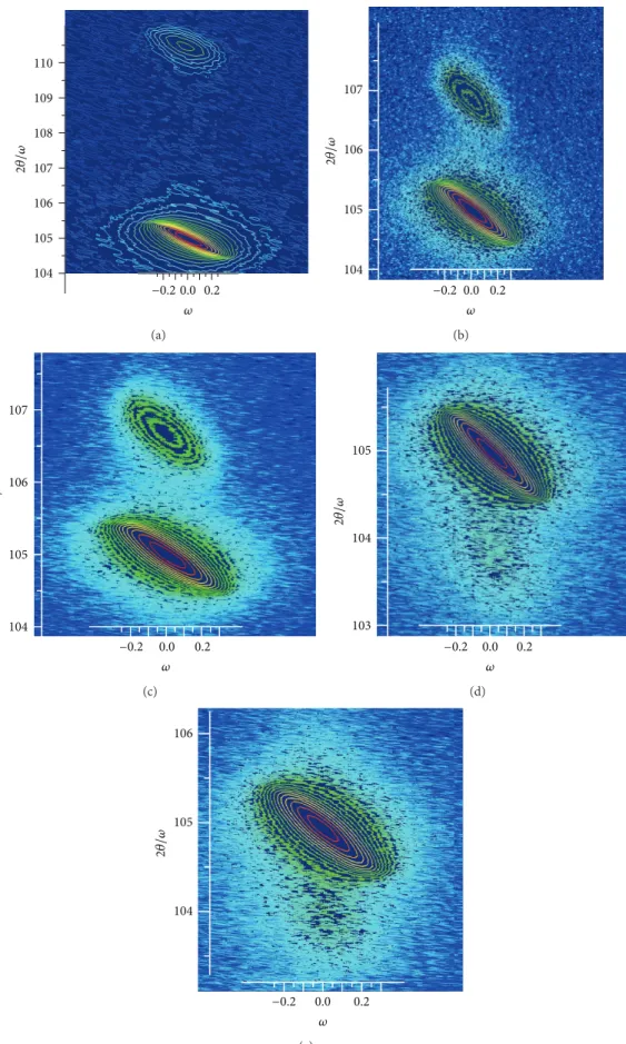
The RSM was performed for both symmetric (0002) and asymmetric (10–15) reflections of the GaN and AlInN layers. The𝜔-2𝜃 HR-XRD RSM of the (0002) and (10–15) reflections of all of the AlInN/GaN (0001)/Al2O3samples are shown in Figures 5and 6, respectively. From the RSM figure of the (0002) and (10–15) reflections, the pole position of the (0002) and (10–15) reflections of the GaN template layers and the AlInN layers can be seen clearly for samples A, B, and C, but for samples D and E, pole position of the AlInN layers could not be seen clearly, because of the close 2𝜃 values of the GaN template layers and AlInN layers. The Indium content, lattice parameters, and strain values in the AlInN layers, in addition to the lattice parameters and the strain values of the
800 700 600 500 400 300 200 100 0 In te n si ty (a.u .)
Azimuths of the (10–15) plane of GaN layer for sample A
−150 −100 −50 0 50 100 150 Φ (deg) (a) In te n si ty (a.u .) −150 −100 −50 0 50 100 150
Azimuths of the (10–15) plane of AlInN layer for sample A
100
50
0
Φ (deg)
(b)
Figure 4: Phi scan curve of asymmetric (10–15) reflection plane of the (a) GaN and (b) AlInN for sample A. Every peak shows azimuths of the (10–15) plane. The diffractive peak repeats every∼60∘.
Table 2: The measured edge and screw type dislocations densities in GaN template layers and the AlInN epilayers are listed.
In content (𝑥) GaN template layers AlInN epilayers
Dscrew(×108cm−2) D
edge(×108cm−2) Dscrew(×108cm−2) Dedge(×108cm−2)
0.04 1.3 4.3 1.7 14.1
0.18 1.0 5.8 1.1 6.7
0.20 1.2 7.2 1.3 7.5
0.47 0.8 2.1 7.3 41.0
0.48 1.0 3.8 6.2 58.0
GaN template layer, were calculated from the RSM around symmetric (0004) and asymmetric (10–15) reflection, whose values are given inTable 1. The𝜀𝑧𝑧and𝜀𝑥𝑥 components for the AlInN epilayers were calculated and given in Table 1. The𝜀𝑧𝑧and𝜀𝑥𝑥values in the AlInN epilayers are one order bigger for samples D(𝑥 = 0.47) and E (𝑥 = 0.48) than the other samples. These results can be attributed to the lattice mismatch between GaN and AlInN with increasing In content in AlInN layer.
The GaN based layers usually grown on lattice mis-matched substrate, such as sapphire, SiC, and Si, cause a high dislocation density. In our case, AlInN epilayers and GaN template were grown on sapphire substrate, which exhibit dislocation density. There are three main types of dislocations present in AlInN epilayers and GaN template layers [8–10,
23,31]:(1) the pure edge type dislocation with Burgers vector 𝑏 = (1/3)⟨11 − 20⟩(⟨𝑎⟩), (2) the pure screw type dislocation with Burgers vector𝑏 = ⟨0001⟩(⟨𝑐⟩), and (3) the mixed type dislocation with𝑏 = (1/3)⟨11 − 23⟩(⟨ 𝑐 + 𝑎⟩). The edge (𝐷edge) and screw(𝐷screw) type dislocation density in the epitaxial layers can be calculated with the equation given below [8–
10,23,31] 𝐷screw=FWHM 2 (0002) 9𝑏2 screw , 𝐷edge= FWHM 2 (10−12) 9𝑏2 edge . (7)
In (7), the FWHM is measured by XRD rocking curves for (0002) and (10–12) reflections and𝑏 is the Burgers vector length (𝑏screw= 5.185 ˚A, 𝑏edge= 3.189 ˚A for GaN and burgers vector for AlInN used from Table 1). The total dislocation density of the AlInN epilayers and GaN template layers is the summation of the edge and screw type dislocation density.
The calculated edge and screw type dislocation densities of the GaN template layers and the AlInN epilayers are given inTable 2. As can be seen inTable 2, the screw type dislocation density in GaN template layers changes between 0.8 × 10⁸(sample D) and1.3 × 108cm−2(sample A), but edge type dislocation densities are a little bit higher than screw type dislocation densities and change between2.1 × 108(sample D) and7.2 × 108cm−2(sample C). The calculated dislocation density values for GaN layers are comparable with GaN, grown on similar buffer structure with MOCVD, reported in literature [8,27]. In addition, the calculated screw and edge type dislocation densities in AlInN epilayers were given in
Table 2. The calculated values of the screw type dislocation
densities in AlInN epilayers were determined to range from 1.1 × 10⁸(sample B) to7.3 × 108cm−2 (sample D). On the other hand, the edge type dislocation densities in the AlInN epilayers change between 6.7 × 10⁸ (sample B) and 5.8 × 109cm−2(sample E). Based on the observations inTable 2,
−0.4−0.2 0.0 0.2 0.4 𝜔 36 35 34 2𝜃 /𝜔 (a) −0.5 0.0 0.5 𝜔 35.0 34.5 34.0 2𝜃 /𝜔 (b) −0.5 0.0 0.5 𝜔 35.5 35.0 34.5 34.0 2𝜃 /𝜔 (c) 35.0 34.5 34.0 33.5 2𝜃 /𝜔 −1.0 −0.5 0.0 0.5 1.0 𝜔 (d) −0.4−0.2 0.0 0.2 0.4 𝜔 35.0 34.5 34.0 2𝜃 /𝜔 (e)
Figure 5: HR-XRD reciprocal space-maps of the (0002) reflection for AlInN/GaN/Al2O3structures with different indium content. In content changes as (a) 4%, (b) 18%, (c) 20%, (d) 47%, and (e) 48%.
104 105 106 107 108 109 110 2𝜃 /𝜔 −0.20.0 0.2 𝜔 (a) −0.2 0.0 0.2 𝜔 104 105 106 107 2𝜃 /𝜔 (b) −0.2 0.0 0.2 𝜔 104 105 106 107 2𝜃 /𝜔 (c) −0.2 0.0 0.2 𝜔 103 104 105 2𝜃 /𝜔 (d) −0.2 0.0 0.2 𝜔 104 105 106 2𝜃 /𝜔 (e)
Figure 6: HR-XRD reciprocal space-maps of the (10–15) reflection for AlInN/GaN/Al2O3structures with different indium content. In content changes as (a) 4%, (b) 18%, (c) 20%, (d) 47, and (e) 48%.
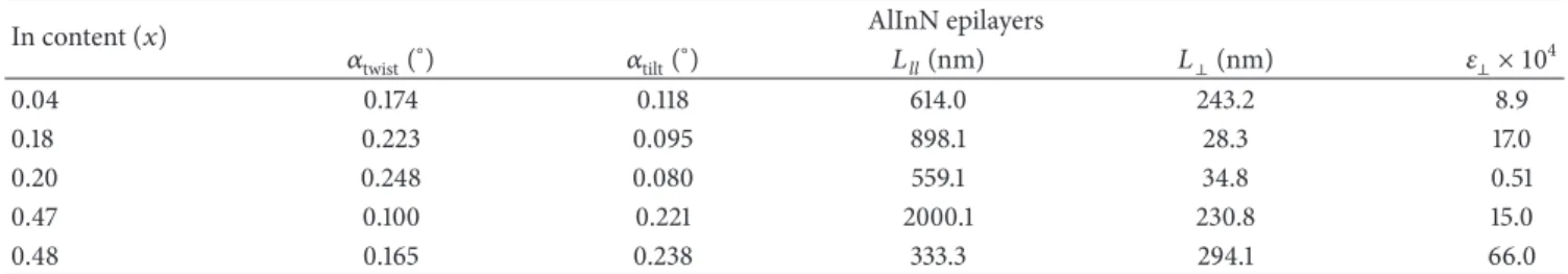
Table 3: The calculated mosaic structures parameters of the AlInN epilayers that were grown on GaN/sapphire structures, including the mean twist angle,𝛼twist, mean tilt angle,𝛼tilt, lateral coherence length,𝐿𝑙𝑙, vertical coherence length,𝐿⊥, and vertical heterogeneous strain,𝜀⊥
are given.
In content (𝑥) AlInN epilayers
𝛼twist(∘) 𝛼tilt(∘) 𝐿𝑙𝑙(nm) 𝐿⊥(nm) 𝜀⊥× 104 0.04 0.174 0.118 614.0 243.2 8.9 0.18 0.223 0.095 898.1 28.3 17.0 0.20 0.248 0.080 559.1 34.8 0.51 0.47 0.100 0.221 2000.1 230.8 15.0 0.48 0.165 0.238 333.3 294.1 66.0
in the AlInN epilayers, both screw and edge type dislocation densities are a little bit higher than in GaN template layers. Moreover, both for sample D and sample E(𝑥 = 0.47 and 0.48), the screw and edge type dislocation densities are higher than the other samples. These cases can be explained with an increasing mismatch in the results of increasing indium content in samples D and E.
AlInN epilayers having a large lattice mismatch with respect to the GaN template layers and substrate form a mosaic structure of slightly misoriented subgrains, which is characterized by the nucleation of slightly misoriented islands and the coalescence of these islands toward a smooth surface [8–10,22–27]. The mosaic blocks can be defined as slightly misoriented with respect to each other. The vertical and lateral coherence lengths, heterogeneous strain, and degree of mosaicity expressed by the tilt and twist angles are important parameters in characterizing the quality of the epitaxial films [8,9,22–30]. The mosaic tilt and twist are defined as the out-of-plane rotation of the blocks perpendicular to the surface normal and the in-plane rotation around the surface normal, respectively [8, 9, 22–30]. The average absolute values of the tilt and twist are directly related to the FWHM of the corresponding distributions of crystallographic orientations [22–27]. The lateral and vertical coherence length, tilt angle, and heterogeneous strain along the c-axis parameters can be calculated from the Williamson-Hall (W-H) plot, and the twist angle from approaches that were proposed by Srikant et al. [25] and Sun et al. [30] or from direct measurement [26,27].
Each contribution to the broadening of particular XRD curves can be separated in a W-H plot [21,23,31]. Specifically in triple-axis diffractometer measurements, the broadening of the rocking curve (𝜔-scan or angular-scan) of the sym-metric (0002), (0004), and (0006) reflections for the epitaxial layer is influenced only by the tilt angle 𝛼tilt and short coherence length parallel to the substrate surface𝐿𝑃[8,9,21,
23].
The (FWHM)𝜔(sin 𝜃)/𝜆 is plotted against (sin 𝜃)/𝜆 for each reflection and fitted by a straight line, where (FWHM)𝜔 is in the angular unit and taken as radians,𝜃 is the Bragg’s reflection angle, and𝜆 is the X-ray wavelength. Then, the mean tilt angle (𝛼tilt) is calculated from the slope of the straight line, and the lateral coherence length (𝐿𝑃= 1/(2𝑦0)) from the inverse of the y-intersection𝑦𝑜of the fitted line with the ordinate.
Because of a small vertical correlation length and a heterogeneous strain along the𝑐-axis causes a broadening of the Bragg reflections in the 2𝜃-𝜔-scan (or radial-scan direction) of the symmetric reflections. These two parameters vertical coherence length (𝐿⊥) and vertical heterogeneous strain (𝜀⊥) can be easily derived from the W-H plot. In the W-H plot,(FWHM)2𝜃-𝜔(cos 𝜃)/𝜆 is plotted against (sin 𝜃)/𝜆 for each reflection and again fitted by a straight line [8,9]. The values of the𝜀⊥ can be estimated directly from the slope (slope =4𝜀⊥) of the line and the𝐿⊥from the𝑦-intersection (𝑦𝑜) the vertical coherence length𝐿⊥can be calculated from the𝑦-intersection (𝑦𝑜) point (𝐿⊥= 0.9/(2𝑦0)).
The W-H plots for symmetric plane ((0002), (0004), (0006)) reflections of the AlInN epilayers were done for the triple-axis𝜔- and 2𝜃-𝜔-scan.Figure 7shows the correspond-ing W-H plots of the AlInN epilayers for the triple-axis (a) 𝜔-scan and (b)2𝜃-𝜔-scan. The straight lines are linear fits to the experimental data. The expected linear behavior of the graphs is experimentally well confirmed, which gives rather accurate tilt angle values.
The 𝛼tilt and 𝐿𝑃 of the AlInN epilayers are shown in
Table 3. The𝛼tilt values of the samples change between the
0.080 and 0.238 degree. As can be seen in table, the𝛼tiltof the samples A, B, and C are similar to each other and rather small. However, with increasing In content, the mean tilt angles increased approx. twofold and measured as 0.221 and 0.238 degree for samples D and E, respectively. Based on the observation of the measured𝛼tiltvalues, it can be concluded that the increased indium content ratio in the AlInN epilayers affects the mean tilt mosaic of the mosaic blocks of the AlInN epilayers.
The 𝐿𝑃 of the AlInN epilayers were determined to range from 559.1 to 2000.1 nm. As can be seen in Table 3, the maximum values were observed for sample D and the minimum values obtained for sample C. The measured𝐿⊥ values for AlInN epilayers are shown inTable 3. The𝐿⊥values for AlInN epilayers range from 28.3 (sample B) to 294.1 nm (sample E). The𝜀⊥ values that were calculated for the GaN template layers and AlInN epilayers for all samples are shown
inTable 3. The maximum𝜀⊥ values in the AlInN epilayers
were obtained for sample E.
Generally, the mean twist angle (𝛼twist) between the subgrains of AlInN and GaN epilayers can be determined from the FWHM of𝜔-scan or Φ-scan XRD curves [8,9,22–
25 20 15 10 5 2 3 4 5 6 sin(𝜃)/𝜆 (nm−1) (FWHM) sin( 𝜃)/ 𝜆 (10 −3nm −1) (0006) (0004) (0002) Sample A Sample B Sample C Sample D Sample E Fit function (a) 35 30 25 20 15 (FWHM) cos( 𝜃)/ 𝜆 (10 −3 nm −1 ) (0006) (0004) (0002) 2 3 4 5 6 Sample A Sample B Sample C Sample D Sample E Fit function sin(𝜃)/𝜆 (nm−1) (b)
Figure 7: W-H plot for AlInN layers. (a) Triple-axis-𝜔-scan and (b) triple-axis 2𝜃-𝜔-scan were measured for the symmetric (000𝑙) (𝑙 = 2, 4, 6) reflections indicated in the figure. The lines result from a linear fit of the data.
the measured double-axis scans data for different(ℎ𝑘𝑙) reflec-tions in a skew symmetric diffraction. Several extrapolation and direct measurements methods have been reported in the literature for a mean twist angle calculation [25,26,28,30]. Srikant et al. [25] and Sun et al. [30] proposed a geometrical model that considers the simultaneous presence of tilt and twist to fit the data from the measurement of 𝜔-scans in skew geometry from reflections with increasing lattice plane inclination (𝜒). Actually, these authors obtained the twist angle by the complicated calculation and fitting method. Metzger et al. [23] just used the FWHM ofΦ-scan for (10– 15) reflection to measure the twist angle. On the other hand, some authors proposed a simple empirical approach to obtain the mean twist angle directly without falling into complicated computation and fitting procedure [26, 27]. In the other measurement method is the grazing incidence in-plane X-ray diffraction (GIIXD) technique, but in this technique a high intensity X-ray source such as a synchrotron and/or special X-ray optics is necessary [35,36].
The FWHM of the rocking curve of an imperfect film is composed of several contributions, such as the mean tilt, twist, the average size of the subgrains, and the inhomo-geneous strain distributions. Although the broadening, due to a limited domain size and inhomogeneous strain, can be significant in highly imperfect films, their effects have been eliminated by using a slit of 0.6 mm that is placed in front of the detector in double-axis 𝜔-scans. Indeed, their contribution to the overall broadening was found to be of minor influence in this measurement case. In addition, the (0002) reflection and (ℎ𝑘𝑙) reflections with either ℎ or 𝑘 nonzero orientation of our samples with triple-axis 2𝜃-𝜔 scans exhibit a small FWHM. The last important point is that
the intrinsic width of the reflection for the crystal and the apparatus broadening for all the experimental reflections are negligible because these effects amount to only a few arcsec. For this reason, we can only measure the broadening that was caused by the twist only by using(ℎ𝑘𝑙) reflections in skew geometry [8–10,27].
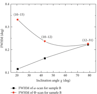
Doubled-axis rocking curves of the𝜔-scans and Φ-scans in different𝜒 were recorded in skew diffraction geometry (𝜔 = 𝜃). InFigure 8, the FWHMs values changes of the𝜔 andΦ-scans with an increasing inclination angle (𝜒) for the sample A were given. The extended FWHMs of 𝜔 and Φ-scans are obtained by using the fit of Pseudo-Voigt function to the rocking curves. It can be seen in this figure that the FWHMs of𝜔-scans increase with the increment of 𝜒, while the FWHM ofΦ scan decreases with the increment of 𝜒 angle. Moreover, they become closer when the (12–31) reflection yields at 78.6∘in𝜒 as seen inFigure 8. In fact, the angle𝜒 reaches 90∘when the reflection plane is perpendicular to the surface of the sample. These results showed that the rocking-curve widths of 𝜔 or Φ scans for this higher 𝜒 angle are close to the twist angles. In every respect, the FWHMs of Φ-scans are larger than those of𝜔-scans with the change of the inclination angle𝜒. Therefore, the mean twist angles must be the average value of the FWHMs of𝜔 and Φ-scans at 𝜒 = 78.6∘.
The measured mean twist angles of the AlInN epilayers are shown inTable 3. The measured mean twist angles of the AlInN epilayers change between 0.100∘and 0.248∘. It can be concluded that the mean twist angles in the AlInN epilayers are close to each other for all the samples. The minimum mean twist angle value was obtained as 0.100∘for sample D, while the maximum mean twist angle was obtained as 0.248∘
20 30 40 50 60 70 80
Inclination angle𝜒 (deg)
0.4 0.3 0.2 0.1 FWHM (deg) (10–15) (10–12) (12–31)
FWHM of𝜔-scan for sample B
FWHM ofΦ-scan for sample B
Figure 8: FWHM ofΦ and 𝜔-scans for (10–15), (10–12), (12–31) reflections, recorded in skew diffraction geometry, of the AlInN layer as a function of the inclination angle𝜒 for sample B (𝑥 = 0.18). FWHMs of𝜔-scan increase with the increment of 𝜒 angle, while those ofΦ-scan decrease. The lines are a guide for the eyes.
for sample C. Based on this observation, it can be argued that the mean twist angle of the AlInN epilayers grown on a GaN template was not strongly affected by the indium content (𝑥) of the Al1−𝑥In𝑥N epilayers.
4. Conclusions
In the present study, Al1−𝑥In𝑥N epitaxial layers, with indium content(𝑥) of 0.04, 0.18, 0.20, 0.47, and 0.48, were grown on GaN template/sapphire structure by MOCVD. The mosaic structures parameters (such as lateral and vertical coherence lengths, tilt and twist angle, and heterogeneous strain) and dislocation densities (edge and screw type dislocations) of the AlInN epilayers and GaN template layers were investi-gated by using XRD measurements. Based on the HR-XRD measurements results, we observed that the mosaic structures parameters, lateral and vertical coherence lengths, tilt and twist angle, and heterogeneous strain of the AlInN epilayers were not strongly affected by indium content(𝑥) in Al1−𝑥In𝑥N epilayers. The screw type dislocation density in GaN template layers changes between0.8 × 108 (sample D) and1.3 × 108cm−2(sample A), but edge type dislocation densities are a little bit higher than screw type dislocation densities and change between2.1 × 108(sample D) and7.2 × 108cm−2(sample C). The calculated values of the screw type dislocation densities in AlInN epilayers were determined to range from1.1×108(sample B) to7.3×108cm−2(sample D). On the other hand, the edge type dislocation densities in the AlInN epilayers are changes between6.7×108(sample B) and 5.8 × 109cm−2(sample E).
Conflict of Interests
The authors declare that there is no conflict of interests regarding the publication of this paper.
Acknowledgments
This work is supported by the European Union under the projects METAMORPHOSE, PHOREMOST, EU-PHOME, and EU-ECONAM, and TUBITAK under Project nos. 105E066, 105A005, 106E198, and 106A017. One of the authors (Ekmel Ozbay) also acknowledges partial support from the Turkish Academy of Sciences.
References
[1] H. Morkoc¸, Nitride Semiconductors and Devices, Springer, Heidelberg, Germany, 1999.
[2] S. Nakamura and G. Fasol, The Blue Laser Diode GaN based
Light Emitters and Lasers, Springer, Heidelberg, Germany, 1997.
[3] F. A. Ponce and D. P. Bour, “Nitride-based semiconductors for blue and green light-emitting devices,” Nature, vol. 386, pp. 351– 359, 1997.
[4] O. Ambacher, “Growth and applications of group III-nitrides,”
Journal of Physics D: Applied Physics, vol. 31, p. 2653, 1998.
[5] E. Arslan, S. Turan, S. G¨okden, A. Teke, and E. ¨Ozbay, “Current-Transport Mechanisms in the AlInN/AlN/GaN single-channel and AlInN/AlN/GaN/AlN/GaN double-channel heterostruc-tures,” Thin Solid Films, vol. 548, pp. 411–418, 2013.
[6] B. S. Eller, J. L. Yang, and R. J. Nemanich, “Electronic surface and dielectric interface states on GaN and AlGaN,” Journal of
Vacuum Science & Technology A, vol. 31, no. 5, Article ID 050807,
2013.
[7] R. S. Pengelly, S. M. Wood, J. W. Milligan, S. T. Sheppard, and W. L. Pribble, “A review of GaN on SiC high electron-mobility power transistors and MMICs,” IEEE Transactions on
Microwave Theory and Techniques, vol. 60, no. 6, pp. 1764–1783,
2012.
[8] E. Arslan, M. K. Ozturk, H. C¸ akmak, P. Demirel, S. ¨Ozc¸elik, and E. Ozbay, “Evolution of the mosaic structure in InGaN layer grown on a thick GaN template and sapphire substrate,” Journal
of Materials Science: Materials in Electronics, vol. 24, no. 11, pp.
4471–4481, 2013.
[9] E. Arslan, M. K. Ozturk, A. Teke, S. Ozcelik, and E. Ozbay, “Buffer optimization for crack-free GaN epitaxial layers grown on Si(1 1 1) substrate by MOCVD,” Journal of Physics D: Applied
Physics, vol. 41, no. 15, Article ID 155317, 2008.
[10] J. S. Speck and S. J. Rosner, “The role of threading dislocations in the physical properties of GaN and its alloys,” Physica B, vol. 24, no. 1–3, pp. 273–274, 1999.
[11] L. Liu and J. H. Edgar, “Substrates for gallium nitride epitaxy,”
Materials Science and Engineering R, vol. 37, no. 3, pp. 61–127,
2002.
[12] J. Xie, X. Ni, M. Wu, J. H. Leach, U. ¨Ozg¨ur, and H. Morkoc¸, “High electron mobility in nearly lattice-matched AlInN/AlN/GaN heterostructure field effect transistors,”
Applied Physics Letters, vol. 91, no. 13, Article ID 132116, 2007.
[13] H. Behmenburg, L. Rahimzadeh Khoshroo, M. Eickelkamp et al., “Influence of barrier thickness on AlInN/AlN/GaN heterostructures and device properties,” Physica Status Solidi C, vol. 6, supplement 2, pp. S1041–S1044, 2009.
[14] G. Liu, J. Zhang, X.-H. Li et al., “Metalorganic vapor phase epitaxy and characterizations of nearly-lattice-matched AlInN alloys on GaN/sapphire templates and free-standing GaN sub-strates,” Journal of Crystal Growth, vol. 340, no. 1, pp. 66–73, 2012.
[15] L. F. Jiang, W. Z. Shen, and Q. X. Guo, “Temperature depen-dence of the optical properties of AlInN,” Journal of Applied
Physics, vol. 106, Article ID 013515, 2009.
[16] T. Aschenbrenner, H. Dartsch, C. Kruse et al., “Optical and structural characterization of AlInN layers for optoelectronic applications,” Journal of Applied Physics, vol. 108, Article ID 063533, 2010.
[17] M. M. Satter, H.-J. Kim, Z. Lochner et al., “Design and analysis of 250-nm AlInN laser diodes on AlN substrates using tapered electron blocking layers,” IEEE Journal of Quantum Electronics, vol. 48, no. 5, pp. 703–711, 2012.
[18] A. Minj, D. Cavalcoli, and A. Cavallini, “Indium segregation in AlInN/AlN/GaN heterostructures,” Applied Physics Letters, vol. 97, Article ID 132114, 2010.
[19] J. J. Zhu, Y. M. Fan, H. Zhang et al., “Contribution of GaN template to the unexpected Ga atoms incorporated into AlInN epilayers grown under an indium-very-rich condition by met-alorganic chemical vapor deposition (MOCVD),” Journal of
Crystal Growth, vol. 348, no. 1, pp. 25–30, 2012.
[20] C. Hums, J. Bl¨asing, A. Dadgar et al., “Metal-organic vapor phase epitaxy and properties of AlInN in the whole composi-tional range,” Applied Physics Letters, vol. 90, no. 2, Article ID 022105, 2007.
[21] G. K. Williamson and W. H. Hall, “X-ray line broadening from filed aluminium and wolfram,” Acta Metallurgica, vol. 1, no. 1, pp. 22–31, 1953.
[22] V. Holy, J. Kubena, E. Abramof, K. Lischka, A. Pesek, and E. Koppensteiner, “X−ray double and triple crystal diffractometry of mosaic structure in heteroepitaxial layers,” Journal of Applied
Physics, vol. 74, article 1736, 1993.
[23] T. Metzger, R. H¨oppler, E. Born et al., “Defect structure of epitaxial GaN films determined by transmission electron microscopy and triple-axis X-ray diffractometry,” Philosophical
Magazine A, vol. 77, p. 1013, 1998.
[24] M. E. Vickers, M. J. Kappers, R. Datta et al., “ In-plane imperfections in GaN studied by x-ray diffraction,” Journal of
Physics D: Applied Physics, vol. 38, no. A99, 2005.
[25] V. Srikant, J. S. Speck, and D. R. Clarke, “Mosaic structure in epitaxial thin films having large lattice mismatch,” Journal of
Applied Physics, vol. 82, p. 4286, 1997.
[26] H. Heinke, V. Kirchner, S. Einfeldt, and D. Hommel, “X-ray diffraction analysis of the defect structure in epitaxial GaN,”
Applied Physics Letters, vol. 77, p. 2145, 2000.
[27] X. H. Zheng, H. Chen, Z. B. Yan et al., “Determination of twist angle of in-plane mosaic spread of GaN films by high-resolution X-ray diffraction,” Journal of Crystal Growth, vol. 255, pp. 63–67, 2003.
[28] H. Li, Y. Luo, L. Wang et al., “Determination of the twist angle of GaN film by high resolution X-ray diffraction,” Applied Physics
Express, vol. 1, Article ID 045004, 2008.
[29] R. Chierchia, T. B¨ottcher, H. Heinke, S. Einfeldt, S. Figge, and D. Hommel, “Microstructure of heteroepitaxial GaN revealed by x-ray diffraction,” Journal of Applied Physics, vol. 93, no. 11, pp. 8918–8925, 2003.
[30] Y. J. Sun, O. Brandt, T. Y. Liu et al., “Determination of the azimuthal orientational spread of GaN films by x-ray diffrac-tion,” Applied Physics Letters, vol. 81, p. 4928, 2002.
[31] M. A. Moram and M. E. Vickers, “X-ray diffraction of III-nitrides,” Reports on Progress in Physics, vol. 72, Article ID 036502, 2009.
[32] P. E. Fewster, “Reciprocal space mapping,” Critical Reviews in
Solid State and Materials Sciences, vol. 22, pp. 69–110, 1997.
[33] M. Schuster, P. O. Gervais, B. Jobst et al., “Determination of the chemical composition of distorted InGaN/GaN heterostruc-tures from x-ray diffraction data,” Journal of Physics D: Applied
Physics, vol. 32, no. 10, p. A56, 1999.
[34] A. F. Wright, “Elastic properties of zinc-blende and wurtzite AlN, GaN, and InN,” Journal of Applied Physics, vol. 82, p. 2833, 1997.
[35] T. A. Lafford, B. K. Tanner, and P. J. Parbrook, “Direct measure-ment of twist mosaic in GaN epitaxial films as a function of growth temperature,” Journal of Physics D: Applied Physics, vol. 36, no. 11, article A245, 2003.
[36] M. S. Goorsky and B. K. Tanner, “Grazing incidence in-plane diffraction measurement of in-plane mosaic with microfocus x-ray tubes,” Crystal Research and Technology, vol. 37, pp. 645–653, 2002.
Submit your manuscripts at
http://www.hindawi.com
Scientifica
Hindawi Publishing Corporation
http://www.hindawi.com Volume 2014 Hindawi Publishing Corporation
http://www.hindawi.com Volume 2014 Hindawi Publishing Corporation
http://www.hindawi.com Volume 2014
Hindawi Publishing Corporation
http://www.hindawi.com Volume 2014
Ceramics
Journal ofHindawi Publishing Corporation
http://www.hindawi.com Volume 2014
Nanoparticles
Journal of Hindawi Publishing Corporationhttp://www.hindawi.com Volume 2014
Hindawi Publishing Corporation
http://www.hindawi.com Volume 2014
International Journal of
Biomaterials
Hindawi Publishing Corporation
http://www.hindawi.com Volume 2014
Nanoscience
Journal ofTextiles
Hindawi Publishing Corporation
http://www.hindawi.com Volume 2014
Journal of
Hindawi Publishing Corporation
http://www.hindawi.com Volume 2014
Crystallography
Journal of Hindawi Publishing Corporationhttp://www.hindawi.com Volume 2014
The Scientific
World Journal
Hindawi Publishing Corporationhttp://www.hindawi.com Volume 2014
Hindawi Publishing Corporation
http://www.hindawi.com Volume 2014
Coatings
Journal of Advances inMaterials Science and Engineering Hindawi Publishing Corporation
http://www.hindawi.com Volume 2014
Hindawi Publishing Corporation
http://www.hindawi.com Volume 2014
Hindawi Publishing Corporation
http://www.hindawi.com Volume 2014
Metallurgy
Journal ofHindawi Publishing Corporation
http://www.hindawi.com Volume 2014
BioMed
Research International
Materials
Journal of Hindawi Publishing Corporationhttp://www.hindawi.com Volume 2014
N
a
no
ma
te
ria
ls
Hindawi Publishing Corporation
http://www.hindawi.com Volume 2014
Journal of