Modulation of Electronic Properties in Laterally and
Commensurately Repeating Graphene and Boron Nitride Composite
Nanostructures
V. Ongun Özçelik,
†,‡E. Durgun,
†,‡and S. Ciraci*
,§†UNAM-National Nanotechnology Research Center, ‡Institute of Materials Science and Nanotechnology, and§Department of
Physics, Bilkent University, 06800 Ankara, Turkey
ABSTRACT: Graphene and hexagonal boron nitride (h-BN) nanoribbons of diverse widths and edge geometries are laterally repeated to form commensurate, single-layer, hybrid honey-comb structures. The resulting composite materials appear as continuous, one atom thick stripes of graphene and BN having the average mechanical properties of constituent structures. However, depending on the widths of constituent stripes they can be metal or semiconductor with band gaps in the energy range of the visible light. These two-dimensional (2D) composite materials allow strong dimensionality in electrical conductivity and undergo transition from 2D to
one-dimen-sional (1D) metal in a 2D medium, resulting in multichannel narrow conductors. As for the composite ribbons, such as one dielectric BN stripe placed between two graphene stripes with bare zigzag edges, charge separation of opposite polarity is possible under applied electricfield and they exhibit resonant tunneling effects at nanoscale. Graphene/BN composite materials also form stable single-wall nanotubes with zigzag or armchair geometries.
■
INTRODUCTIONRealization of two-dimensional (2D) systems three decades ago, where electrons are propagating in 2D, but confined in the third dimension (3D) showed quantization that is different from 3D systems. This led to novel electronic properties such as multiple quantum wells, resonant tunneling, integer and fractional quantum hall effects, etc.1−4 The synthesis of
graphene5,6 with one atom thick honeycomb structure has added even more unusual features like massless Dirac Fermion behavior and electron−hole symmetry while clarifying earlier conjectures pointing structural instabilities in 2D systems. Subsequently, the past decade has witnessed an active search for new 2D structures, as well as their bi- and multilayers for novel technological applications. What followed graphene were other 2D materials, each with different unusual properties, such as the 2D insulator boron-nitride (h-BN);7−9 graphene analogues of silicon and germanium atoms;10−13 h-BN analogues of Group IV−IV, III−V, and II−VI compounds;14 graphyne;15−17 transition-metal dichalcogenides;18−21 and the auxetic piezoelectric 2D material silicatene with negative Poisson’s ratio.22 Additionally, these 2D materials have been functionalized by the coverage of adatoms like hydrogen, oxygen, fluorine, and transition metal atoms. In particular, functionalization by host adatoms resulting in exotic local reconstruction and phases, like dumbbell structures of silicene and germanene13,23−28was shown to lead layered structures of silicon.29−31
Diverse composite bilayer and multilayer structures have been fabricated by vertical stacking of different monolayer
materials (like graphene and h-BN or graphene and MoS2or different dumbbell based phases of silicene).12,29,31−33 The fabrication of graphene on h-BN was initially succeeded using mechanical transfer method.6Actually, graphene and h-BN are almost lattice matched, and they can also grow on top of each other.34,35 Interplane heterostructures obtained by vertical stacking of graphene and h-BN single-layers structure are of particular importance because of their use in the nanoscale electronic devices such as memory devices, field effect transistors and capacitors.32,36,37 In particular, h-BN layers capped by two parallel graphene layers display a capacitive behavior where the predicted capacitance values are in the range of supercapacitors. These systems were shown to exhibit thickness dependent quantum effects at small separations, but to act as a classical Helmholtz capacitor at large thicknesses of h-BN.36Notably, the process of vertical stacking is reminiscent of modulated doping or multiwell quantum heterostructures like AlGaAs4and pseudomorphic Si(p)/Ge(q) superlattices.38
As an alternative way to functionalize single layer honeycomb structures and hence to fabricate new materials, the formation of 2D patterned domains of one type of material embedded in another material has been proposed.39−41 Not only domains but also periodically repeating defects and adatom islands can be considered to construct mesh structures. Recent advances have made the mesh configuration a controllable parameter for
Received: February 16, 2015
Revised: May 21, 2015
Published: May 21, 2015
Article
monitoring physical properties of nanostructures.42−45 Specif-ically, in-plane graphene/h-BN hybrid structures have attracted considerable interest because of their potential applications in flexible 2D optoelectronic devices.32,33,46−49The realization of
monolayer materials consisting of hybrid graphene/h-BN domains has motivated further research in the field.50 Subsequently, graphene/h-BN in-plane heterostructures with controllable widths down to 100 nm have been fabricated using lithographic patterning and sequential CVD growth of graphene.51 Anomalous insulator−metal transition has been observed in graphene/h-BN hybrid structures, such as BN nanoribbons or nano domains embedded in graphene.52 Theoretically, half-metallicity has been predicted in hydrogen saturated hybrid graphene/h-BN nanoribbons.53
In this paper we consider one-atom-thick composite materials that are composed of laterally and periodically repeating, zigzag or armchair nanoribbons that are merged commensurately as stripes in a single layer honeycomb structure. Our model is described in Figure 1a,b. While the model has translational periodicity of the honeycomb structure along thex-direction, the translational periodicity along the y-direction depends on the widths of adjacent graphene and h-BN stripes in terms of the number of C and B+N atoms in the unit cell; p and q, respectively. We name these hybrid structures as graphene/BN composites abbreviated as G(p)/BN(q) in the rest of the paper. We distinguish diverse types of features and functionalities in different types of G(p)/BN(q) composites having zigzag or armchair geometry. As schematically described in Figure 1c, these are BNδ-doping in wide graphene stripes; electronically decoupled one-dimensional (1D) composites in a 2D framework consisting of wide graphene and wide h-BN stripes; grapheneδ-doping in wide h-BN stripe; and finally line compounds where each unit cell contains one graphene and one BN hexagon.
We carried out a systematic analysis of electronic structure showing that the electronic and functional properties of these one-atom-thick composites can be tuned by altering the p/q ratio and boundary geometry of the constituents; they can be metal or semiconductor in the energy range of visible light. We find that (i) when their widths are increased, the constituent stripes become electronically decoupled and in a 2D composite system a transition from 2D to 1D takes place, whereby electronic states become confined to 1D stripes. Such structures can form multiple quantum wells. (ii) However, when the widths of both stripes (p and q) are decreased, they start to couple and hence the composite material behaves as a compound composed of lines of different materials and displays unique characteristics. The electronic structure acquires 2D dispersion; not only along the stripes, but also in the transversal direction. (iii) The properties of one constituent alone can be modified by the δ-doping of the other constituent. (iv) Remarkably, the ribbon of composite material, such as BN(q) capped by G(p) from both side allows charge separation of opposite polarity and makes energy storage possible under the external electric field along y-direction.36 These ribbons also undergo metal insulator transition under applied electric field and can function as resonant tunneling double barrier.3 (v) Stable, single-wall nanotubes can be constructed from G(p)/ BN(q) zigzag and armchair nanoribbons. Briefly, a compre-hensive analysis of the dimensionality of electronic structure of a 2D monolayer, composite G(p)/BN(q) material is presented, and novel features are revealed. Additionally, this study includes an extensive analysis of the energetics related to the hybrid graphene/BN structures.
■
METHODOur predictions are obtained from state of the art first-principles pseudopotential calculations based on the spin-polarized density functional theory (DFT) within the
Figure 1.Composite materials, which consist of laterally repeating, commensurate graphene and h-BN nanoribbons merged in a single layer honeycomb structure and hence form stripes along the x-direction. (a) G(p)/BN(q) composite composed of zigzag graphene and h-BN nanoribbons, which are stripes periodically repeating along they-axis. The unit cell of the composite structure is delineated by dashed lines. Numbers of C and B+N atoms in the unit cell arep = 4 and q = 4, respectively. (b) Same for armchair graphene and h-BN nanoribbons with p = 8 and q = 8. (c) Schematic description of the band diagrams in the direct space with conduction band (CB) and valence band (VB) edges. The band gaps are shown in between. Four different combinations are schematically described: (i) BN δ-doping in graphene; (ii) a composite structure composed of 1D, wide graphene and h-BN stripes; (iii) grapheneδ-doping in h-BN; (iv) the line compound. Band gaps depend on the values of p and q, as well as the geometries of the border between stripes. (d) An MD snapshot of the 4× 3 supercell of a zigzag line compound taken at T = 1000 K after 5 ps. (e) Same for the 3× 2 supercell of an armchair line compound. In the ball and stick representations, C, B, and N atoms are shown by brown, green, and blue balls, respectively.
generalized gradient approximation (GGA) including van der Waals corrections.54 We used projector-augmented wave potentials (PAW)55 and the exchange-correlation potential is approximated with Perdew−Burke−Ernzerhof (PBE) func-tional.56 The Brillouin zone (BZ) was sampled in the Monkhorst−Pack scheme, where the convergence in energy as a function of the number of k-points was tested. The k-point sampling of (21× 21 × 1) was found to be suitable for the BZ corresponding to the primitive unit cell of G(4)/BN(4) composite with zigzag edge. For wider stripes and hence larger unit cells, this sampling has been scaled accordingly. The number of k-points were further increased to (48× 48 × 1) in the projected density of states calculation. Atomic positions were optimized using the conjugate gradient method, where the total energy and atomic forces were minimized. The energy convergence value between two consecutive steps was chosen as 10−5eV. A maximum force of 0.01 eV/Å was allowed on each atom. Numerical calculations were carried out using the VASP software.57 To achieve charge separation of opposite polarity on composite nanoribbons under transversal external electricfield, the structure optimization and self-consistent field charge density calculations are performed using SIESTA software with numerical local basis set.58 This way, spurious divergences emerging from the use of plane wave basis set with periodic boundary conditions are eliminated.59,60
Since the band gaps are underestimated by standard DFT, we also carried out calculations using the HSE06 hybrid func-tional,61,62 which is constructed by mixing 25% of the Fock
exchange with 75% of the PBE exchange, and 100% of the PBE correlation energy and range separation parameter is set to 0.2. The stability of composite structures are tested by ab initio molecular dynamics (MD) calculations carried out at finite temperatures. A Verlet algorithm is used to integrate Newton’s equations of motion with time steps of 2 fs. Starting from 200 K we carried out MD calculations for 1 ps at temperatures of 200, 400, 600, 800, and 1000 K, continuing and lasting for 5 ps in total for each system. To maintain the system in the desired constant temperature the velocities of atoms are rescaled in each time step.
■
RESULTS AND DISCUSSIONBare zigzag graphene nanoribbon ZGNR(p) and bare h-BN nanoribbon ZBNR(q) are metallic. When their edges are saturated by hydrogen atoms, the zigzag h-BN nanoribbon transforms into an insulator.9Also, when the same ZBNR joins graphene nanoribbons commensurately at both side, it becomes an insulator with a wide band gap. When carbon atoms at the edges of ZGNR(p) are saturated by B and N edge atoms of ZBNR(q) at alternating sides, ZGNR(p) changes into a semiconductor, where the band gap diminishes asp increases. On the other hand, bare armchair graphene nanoribbon, AGNR(p) is a semiconductor with a band gap that generally decreases with increasing p. At the same time, the band gap shows family behavior according top = 3n + m; namely, the band gap is the largest for m = 0, smallest for m = 2, and intermediate form = 1 for a given integer n.63However, this
Figure 2.Electronic structure of various combinations of G(p)/BN(q) composite materials forming stripes along the x-direction in a single layer honeycomb lattice. (a) Line compound G(4)/BN(4) with zigzag border. Contributions of graphene (red) and h-BN (turquoise) stripes to energy bands are mimicked by the size of small rectangles tracing the bands. The rectangular Brillouin zone and its relevant symmetry directions are shown by the inset. (b) Projected density of states (P-DOS) projected to C−N, C−B bonds at the borders of stripes and C−C, B−N bonds within graphene and h-BN stripes. The border atoms are delineated in a rectangle. (c) Isosurfaces of the total electronic charge density,ρ(r). (d) Energy bands of composite G(28)/BN(28) with zigzag borders. (e) P-DOS. (f) Isosurfaces of the total charge density. (g−i) Same for the line compound G(8)/BN(8) with armchair border. (j−l) Same for G(32)/BN(32) composite with armchair border.
situation is subject to change in G(p)/BN(q) composite structure with armchair borders.
Energetics and Stiffness. The zigzag border of a G(p)/ BN(q) comprises one type of bond only; one side C−B bond, and the other side C−N bond. In this respect, the energetics of the zigzag border between graphene and h-BN is crucial for lateral epitaxial growth. Here we present an analysis of energetics, which may be critical for the growth of graphene/ BN composite materials.
The substitutions of both B and N in 5 × 5 graphene are endothermic, and the substitution energies are calculated as −2.64 eV and −3.59 eV, respectively. Accordingly, the substitution of C atom in graphene is easier by B atom than by N atom. Next, we examine the adsorption of B and N atoms to the zigzag edges of bare graphene nanoribbons. We first consider the adsorption of isolated, single B or N to ZGNR(16). The calculated binding energy of the isolated, single B (N) atom to the carbon atom at the zigzag edge is 6.19 eV (6.86) eV. The binding energies are positive since the adsorption of B or N is an exothermic process. In compliance with the substitution energies discussed above, the N atom forms a relatively stronger bond. We also consider the situation where one edge of ZGNR(16) is fully covered either by B or by N atoms. Here the binding energies are given by including and also by excluding the adsorbate−adsorbate (namely, B−B or N−N coupling). The binding energy of full B (N) coverage of one edge is found to be 4.79 eV (6.19 eV) if the adsorbate− adsorbate coupling is included. Conversely, the binding energy
of B (N) is calculated to be 6.4 eV (6.08) eV if the adsorbate− adsorbate coupling is excluded. Here the adsorption of N in two cases displays an opposite trend as compared to that of B atom, since its magnetic state is different when compared to the isolated case.
Another critical energy to be addressed is associated with the commensurately grown, single ZGNR(p)+ZBNR(q) composite nanoribbon, which is treated within the supercell method using the prototype ZGNR(12)+ZBNR(12) ribbon. Here one distinguishes two cases: In thefirst one, ZBNR(12) is attached to ZGNR(12) through its B atoms located at one of the edges and thus forms C−B bonds at its border with graphene. In the second case, ZBNR(12) is attached to ZGNR(12) through its N atoms to form C−N bonds at the border. Through the difference of the total energies calculated for these two cases (ET[B−C] = −210.06 eV and ET[C−N] = −209.94 eV), we
found that the formation of C−B bonds between two commensurately grown ZGNR(12) and ZBNR(12) nanorib-bons is favored by 0.13 eV per bond relative to C−N bond. This conclusion agrees with the recent experimental data.49 Two types of bonds, C−B and C−N, coexist at either borders of armchair geometry.
The in-plane stiffness, which is commonly used to measure of strength for 2D materials, can be expressed as C = (1/Ao)×
(∂2Es/∂ϵ2), whereEsis the strain energy,Aois the equilibrium
area, andϵ is the axial strain calculated by Δax,y/ax,y,a being the
lattice constant in thex or y direction. The calculated in-plane stiffness values of the composite materials approximately
Figure 3.δ-doping of a wide graphene stripe by the narrow h-BN stripe with zigzag or armchair border and vice versa. (a) Electronic band structure of the wide graphene stripe, which isδ-doped by the narrow BN stripe with zigzag border, i.e., G(28)/BN(4). (b) Density of states projected to C− B, C−N bonds at the borders highlighted by rectangles, and C−C, B−N bonds within graphene and h-BN stripes. (c) Isosurfaces of the total charge density. (d−f) Same for a wide BN stripe, which is δ-doped by the narrow graphene with zigzag border, i.e., G(4)/BN(28). (g−i) Same for a wide graphene stripe, which isδ-doped by the narrow BN stripe with armchair border, G(32)/BN(8). (j−l) Same for a wide BN stripe, which is δ-doped by the narrow graphene with armchair border, G(8)/BN(32).
correspond to the average of the in-plane stiffness of pure constituents (grapheneCG= 330 N/m2, h-BNCBN = 255 N/
m2); namely, C¯=(p × CG + q × CBN) /(p + q) . We also
calculateC¯ = 290 N/m2forp = 4, q = 4, which is rather high.
In fact, it is higher than that of silicene (62 N/m2)14and MoS2
(138 N/m2).21
The stability of a 2D prototype line compound of zigzag and armchair composite structure is tested by ab initio MD calculations up toT = 1000 K. Both composite structures remained stable, except atomic planes became wavy, as shown in Figure 1d,e.
Line Compound. In Figure 2a, line compound G(4)/ BN(4) with zigzag border is a semiconductor with a band gap of 1.2 eV. The effective mass, mx,y* =ℏ2[d2E
n(kx,y)/dkx,y2]−1, of
electrons and holes is small forkx, but large forky, resulting in
conductivity alongx-direction much higher than that along y-direction; namely,σx≫ σy. As shown by the bands in Figure 2a,
and by the density of states projected to C−B, C−N bonds at the border and C−C, B−N bonds within the graphene and h-BN stripes in Figure 2b, states at the valence band originate mainly from C−B bond and C−C bonds, while the states at the edge of conduction band are constructed from C−N bonds. The gap between bands constructed from pure B−N bonds is ∼6 eV. Because of coupling between graphene and h-BN stripes, G(4)/BN(4) is a compound and is considered to be a unique material, whereby line-like, narrow graphene and h-BN stripes extend along the x-axis. As shown in Figure 2c significant amount of charge is transferred from C to N and from B to C at the alternating borders of h-BN stripes. Similar behavior also occurs in armchair line compound, which is also a semiconductor with a direct band gap ofEg= 1.7 eV as shown
in Figure 2g−i. The states at the edges of the valence and conduction band are constructed from C, B, and N atomic orbitals. Clearly, armchair G(8)/BN(8) is a compound of graphene and h-BN with unique features.
Composite Structures. In Figure 2d−f, zigzag G(28)/ BN(28) composite displays rather different behavior; we see that graphene and BN states are separated in direct space. h-BN states form an insulator with a band gap of∼6 eV. A small gap occurs along K−X and also the X−Γ direction between bands originating from the C−N and C−B bonds. Even if these two bands appear to have very small gap of 0.04 eV at a specific k-point along theΓ−X direction, they are physically separated in the direct space. However, if a small number of electrons could be accommodated at the minimum of the conduction band through tunneling or doping, a strictly 1D band originating from C−N bond states can be conducting along the stripes. This feature can be used as a switch operating under appliedfield along the y-direction. A direct band gap of ∼1 eV occurs between the bands in graphene along theΓ-K direction. The situation with G(32)/BN(32) armchair composite in Figure 2 j−l is different; graphene stripes behave as a 1D narrow band gap semiconductor nearΓ-point, while h-BN is an insulator. Upon modulating the doping, namely, donors in h-BN stripe, such a composite structure can be used to construct a multichannel conductor between two electron reservoirs with quantized conductance. Alternatively, one can construct electron channels with hornlike entrances and exits at the ends of stripes, and can attain adiabatic evolution of channel states. Briefly, we believe that armchair composite structures can be utilized to realize diverse geometries yielding some fundamental quantum effects.
δ-Doping of Graphene and BN. The electronic structure of wide G(p) stripe, which is δ-doped by BN(4) is presented in
Figure 3a−c for zigzag border. h-BN bands with large band gap are separated from graphene states. The h-BN stripe is too narrow, and hence two bands corresponding to zigzag edge states originating from the C−N and C−B bonds cross each other along Γ−X at the Fermi level. This attributes a 1D metallic character to the graphene stripe, even if the narrow BN stripe poses a thin potential barrier with its wide band gap. This situation is clearly seen by the high state density at the Fermi level as presented in Figure 3b. On the other hand, a wide stripe of h-BN(q) with zigzag border, which is δ-doped by G(4), is a narrow band gap semiconductor along they-direction with a band gap of∼0.7 eV, as shown in Figure 3d−f. The gap occurs between the bands derived from C−N and C−B bonds. Since the potential barrier set by h-BN is high and wide, electron due to dopants (holes due to acceptors) confined to narrow quantum wells of the conduction (valence) bands of graphene stripe can exhibit strictly 1D character.
In Figure 3g−i, the wide graphene stripe G(p), which is δ-doped by a narrow BN(8) stripe with armchair edge is a narrow band gap semiconductor. The band gap is, however, large along theK−X direction perpendicular to the stripes. The gap region is dominated by graphene bands, while bands associated with BN(8) occur∼3.5 eV below and ∼3.5 eV above the Fermi level and pose a narrow but high barrier for tunneling between nearest graphene stripes. Conversely, wide BN(q), which is δ-doped by narrow G(8) with armchair border, has BN bands separated by a wide band gap of∼6 eV as shown in Figure 3j−l. In this band gap, the bands associated with G(8) have relatively smaller band gap at the center of the BZ and also have low density of states.
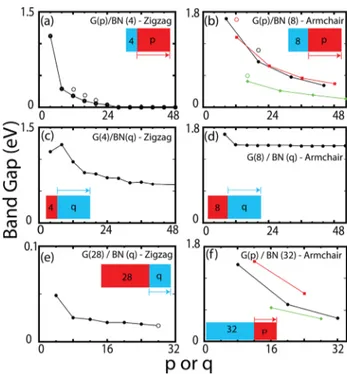
Variation of band gaps of different G(p)/BN(q) composite with zigzag or armchair border are summarized in Figure 4. As shown in Figure 4a, a wide graphene stripe, which isδ-doped by BN(4) with zigzag border, namely, G(p)/BN(4) attains metallic behavior forp > 24. This conclusion is also confirmed
Figure 4.Variation of band gaps for different G(p)/BN(q) composites with zigzag or armchair borders. Band gaps calculated by HSE method are indicated by empty circles.
by HSE calculations. In Figure 4b, G(p)/BN(8) with armchair border remains a semiconductor, even for largep and has band gapEgranging from 1.7 to 0.1 eV asp increases. However, the
calculated values of band gap trace are always the lowest value whenp − 4 is an integer multiple of 3 (4 being the number of C atoms at the armchair border). This is a well-known family behavior of graphene armchair nanoribbons, but is realized in the reverse order of the free armchair graphene nanoribbons. The band gap of the wide BN(q) stripe, which is δ-doped by G(4) stripe with zigzag border is large for smallq, but decreases and eventually saturates at∼0.5 eV as q increases in Figure 4c. By contrast, the band gap of BN(q) with armchair border, which isδ-doped by G(8), is not affected by the width of the h-BN stripe and quickly saturates at a value Eg = 1.45 eV, as
shown in Figure 4d. In Figure 4e, G(p)/BN(q) composites with zigzag border, where graphene and h-BN states are physically separated and confined to their own region are always semiconductors with very small band gaps no matter what the values of p and q are. However, the band gaps of these composites with armchair border in Figure 4f show family behavior in the energy range from 1.7 to 0.3 eV depending on the value ofp. The largest gap values occur when p is an integer multiple of 3 and smallest values occur whenp − 4 is an integer multiple of 3. As noted earlier, the family behavior of band gaps, which is indigenous to armchair graphene nanoribbons occurs in reversed order in G/BN composite structure here. Band gap values of selected compounds calculated by HSE method are also shown in Figure 4 by empty circles.
Graphene/BN Composite Nanoribbons. Finally, it should be noted that the properties of 2D composites outlined above can be multiplied through (hybrid) composite ribbons consisting offinite number of commensurately grown ZGNR-(p) [AGNR(p)] and ZBNR(q) [ABNR(q)] nanoribbons with bare or hydrogen saturated edges. The edge geometry and ordering of nanoribbons, the edge saturation by foreign and host atoms, and their sizep and q offer so many parameters to monitor their electronic and magnetic properties. These composite nanoribbons or in-plane heterostructures have been fabricated, and their potential as field effect transistor and split closed loop resonator have been explored.33,50,51Here we present an interesting feature of composite nanoribbons, which may lead to various technological applications. For example, a single-layer ZGNR(p)+ZBNR(q)+ZGNR(p) com-posite and commensurate nanoribbon that is composed of one dielectric nanoribbon of BN placed between two metallic graphene nanoribbons with zigzag edge can allow charge separation of opposite polarity under an external electricfield, Eyapplied along they-direction and hence can lead to energy
storage. The configuration of this device is described in Figure 5a. The atomic structure is optimized for a given external electric field Ey, and the excess charge in the left and right
graphene stripes ± Q(Ey) is calculated from the difference charge density,Δρ (r, Ey) =ρ(r, Ey)− ρ(r, Ey= 0) . Here,ρ(r, Ey) is the self-consistent charge density of the device calculated
for a given Ey. In Figure 5a, we also show the isosurfaces of
difference charge density. The variation of q(Ey) as a function
of Ey is given in Figure 5b. Once the charge separation of
opposite polarity is attained under the externalfield Ey, it can be kept for a long time, even if Ey → 0, since the insulating
ZBNR(q) hinders the tunneling of electrons from left to right. Alternatingly, one can also construct double well resonant tunneling structures, ZGNR(p)+ZBNR(q)+ZGNR(p) with
interesting resonant tunneling effects and multiple quantum well structures, even Wannier ladders.
Here we address the questions of whether the application of the external electric field in the range of 1 V/Å might be unrealistically high or whether ZGNR( p)+ZBNR(q)+ZGNR-(p) composite nanoribbon will breakdown/discociate even if such high fields are realized in an experiment. Previously, diffusion of H atom on graphene under an external field of 0.01 a.u. (=0.5 V/Å) was studied and no instability in the graphene layer was reported.64 Similarly, dissociative adsorption of hydrogen on nitrogen-doped graphene was studied under the electricfield values ranging between 0 and 0.5 V/Å.65Neither of these theoretical studies report breaking of the carbon− carbon bonds in graphene under electric field values in the range of 1 V/Å. Furthermore, in another theoretical study investigating the tuning of electronic and magnetic properties of H- and F-doped graphene even higher electricfield values up to approximately equal to 10 V/Å were used on graphene without any instability.66Similarly, an in-plane electricfield in the range of 0.15 V/Å was used for the alignment of graphene nanoribbons.67Experimental studies controlling the rippling or
Figure 5.(a) Atomic configuration of ZGNR(p)+ZBNR(q)+ZGNR-(p) composite ribbon with p = 4, q = 4. External electric field Ey is applied along y-direction in the plane of the composite ribbon extending along thex-direction. Top and side views of the isosurfaces of the difference charge density Δρ(r, Ey) show that the left ZGNR(p) is negatively charged, while the right graphene is positively charged. (b) Variation of excess charge accumulated in graphene nanoribbons at both side of BN,Q with the applied electric field Ey. (c) Snapshot taken from the MD simulation of the nanoribbon at 300 K under external electricfield.
work function of graphene suggest that graphene can withstand electricfields in the order of 1 V/Å.68,69
To test the stability of the composite ZGNR( p)+ZBNR-(q)+ZGNR(p) nanoribbon, we performed ab initio molecular dynamics calculations at 300 K under Ey = 1 V/Å using the
Verlet algorithm. The nanoribbon remained stable after 2 ps, as can be seen from the snapshot presented in Figure 5c . To increase the degrees of freedom for possible reconstruction, we also repeated the same simulation in a larger (3× 1) unit cell at 500 K. The nanoribbon continued to maintain its stability after 4 ps simulation. Additionally, we carried out ab initio total energy calculations to estimate the weakening of bonds under the external electricfield. The energy of the ribbon increased by 1.2 eV per cell (i.e., per 6 C atoms +3 B + 3 N atoms amounting to 17 bonds) underEy= 1 V/Å. Since the cohesive
energies of pristine graphene and h-BN are calculated to be 16.2 eV/cell (per 2 C atom) and 14.5 eV/cell (per B+N atoms), respectively, the average bond energy is 5.12 eV. Accordingly, the bonds are weakened by less than 2% under the appliedEy= 1 V/Å. This is rather small and does not give rise
to any instability.
Graphene/BN Nanotubes. Not only ribbons, but also nanotubes can be realized with stripes of graphene and h-BN, which are parallel (or perpendicular) to the axis of the tube. Prototype nanotubes are constructed by rolling G(32)/BN(32) zigzag and G(48)/BN(48) armchair nanoribbons at specific chiral angles as shown in Figure 6a,b. Following the (n,m) labeling notation for single-wall carbon nanotubes (SWNTs), these nanotubes correspond to (8 × 0) zigzag and (6 × 6) armchair nanotubes, where the integers n and m denote the
number of unit vectors along two directions in the honeycomb crystal lattice. Upon relaxation both of the nanotubes remain stable. The strain energy (compared to planar structure) is calculated to be 1.56 eV/cell and 1.64 eV/cell for (8× 0) and (6× 6) nanotubes, respectively. When electronic properties are considered, SWNT can be a metal or semiconductor depending on (n,m) or chiral angle. Interestingly, unlike SWNTs, both (8 × 0) and (6 × 6) nanotubes are semiconductors with band gaps ofEg= 0.98 eV and Eg= 1.49 eV, respectively. Briefly,
single-walled nanotubes of G(p)/BN(q) composite materials bring new options over the nanotubes of these constituents.
■
CONCLUSIONIn conclusion, we predict novel electronic structures of 2D composite (hybrid) materials of laterally repeating graphene and h-BN stripes, G(p)/BN(q) with zigzag or armchair border, which form commensurate, one-atom-thick, single-layer honey-comb structures. In spite of the fact that h-BN is a wide band gap insulator and graphene is a semimetal, G(p)/BN(q) composite can display diversity of electronic properties. Depending on the composition of p and q, as well as the edge geometry between stripes, they can be a 1D metal, a semiconductor with the band gap in the visible range, and semiconductor heterostructures showing periodic band gap modulation in direct space. For a specific combination of p and q, phase separation is attained with interesting transition from 2D to 1D in a 2D system. By making special combination and sequences of p and q (and their graded sequences), one can also achieve graded band gap in direct space for novel optical properties. Specifically, the δ-doping of a wide stripe of graphene (BN) by the narrow BN (graphene) stripe results in unusual modifications in the electronic structure. Bi- or multilayers of composites with displaced or in-registry geometry, even with finite rotation angle between atomic planes give rise to unusual electronic properties. The novel and fundamental aspects of our study are emphasized by way of conclusion:
(i) While previous studies dealt with 1D aspects of lateral graphene/BN heterostructures, the present study reveals 1D, as well as interesting 2D aspects together with the transition between 1D to 2D dimensionality, which were unknown before. (ii) An extensive analysis of electronic structure for laterally repeating (periodic) graphene/BN heterostructures with varying widths is performed, which is essential for the understanding of these heterostructures and their applications. (iii) The concept of δ-doping and their dramatic effects to modify the electronic structures has been introduced to in-plane heterostructures. (iv) The charge separation in graphene/ BN/graphene nanoribbons under the in-plane, external electric field leading to interesting applications. Based on ab initio calculations, it has been shown that the nanoribbon can remain stable under the application of high electricfields.
It should be noted that similar in-plane heterostructures can be produced between lattice matched, single-layer transition metal dichalcogenides21 (such as MoS2(p)/WS2), III−V
compounds14 (such as GaN(p)/AlN(q)), pseudomorphic silicene(p)/germanene(q)11 or silicene(p)/phosphorene(q), yielding a manifold of electronic and magnetic properties. Consequently, composite structures with their planar single and multilayers, composite nanoribbon and tubular forms keep the promise of developing a way of designing novel electronic and magnetic materials.
Figure 6. (a) Zigzag (8 × 0)-G(32)/BN(32) nanotube and its calculated energy band structure. (b) Armchair (6 × 6)-G(48)/ BN(48) nanotube and its energy band structure. Band gaps are shaded. The zero of energy is set to the top of the valence band.
■
AUTHOR INFORMATIONCorresponding Author
*E-mail: [email protected].
Notes
The authors declare no competingfinancial interest.
■
ACKNOWLEDGMENTSThe computational resources were provided by TUBITAK ULAKBIM, High Performance and Grid Computing Center (TR-Grid e-Infrastructure). V.O.Ö. and S.C. acknowledge financial support from the Academy of Sciences of Turkey (TUBA). This work is partially supported by TUBITAK under the Project No. 113T050. E.D. acknowledges support from Bilim Akademisi - The Science Academy, Turkey, under the BAGEP program.
■
REFERENCES(1) Klitzing, K. The Quantized Hall Effect.Rev. of Mod. Phys. 1986, 58, 519−531.
(2) Tsui, D. C.; Stormer, H. L.; Gossard, A. C. Two-Dimensional Magnetotransport in the Extreme Quantum Limit. Phys. Rev. Lett. 1982,48, 1559.
(3) Chang, L.; Esaki, L.; Tsu, R. Resonant Tunneling in Semiconductor Double Barriers.Appl. Phys. Lett. 1974, 24, 593−595. (4) Mendez, E.; Esaki, L.; Wang, W. Resonant Magnetotunneling in GaAlAs−GaAs−GaAlAs Heterostructures. Phys. Rev. B 1986, 33, 2893. (5) Novoselov, K. S.; Geim, A. K.; Morozov, S.; Jiang, D.; Zhang, Y.; Dubonos, S.; Grigorieva, I.; Firsov, A. Electric Field Effect in Atomically Thin Carbon Films.Science 2004, 306, 666−669.
(6) Geim, A. K.; Novoselov, K. S. The Rise of Graphene.Nat. Mater. 2007,6, 183−191.
(7) Novoselov, K.; Jiang, D.; Schedin, F.; Booth, T.; Khotkevich, V.; Morozov, S.; Geim, A. Two-dimensional Atomic Crystals.Proc. Natl. Acad. Sci. U.S.A 2005, 102, 10451−10453.
(8) Pacile, D.; Meyer, J.; Girit, C. O.; Zettl, A. The Two-dimensional Phase of Boron Nitride: Few-Atomic-Layer Sheets and Suspended Membranes.Appl. Phys. Lett. 2008, 92, 133107−133107.
(9) Topsakal, M.; Aktürk, E.; Ciraci, S. First-Principles Study of Two-and One-Dimensional Honeycomb Structures of Boron Nitride.Phys. Rev. B 2009, 79, 115442.
(10) Durgun, E.; Tongay, S.; Ciraci, S. Silicon and III-V Compound Nanotubes: Structural and Electronic Properties.Phys. Rev. B 2005, 72, 075420.
(11) Cahangirov, S.; Topsakal, M.; Aktürk, E.; Şahin, H.; Ciraci, S. Two- and One-Dimensional Honeycomb Structures of Silicon and Germanium.Phys. Rev. Lett. 2009, 102, 236804.
(12) Vogt, P.; De Padova, P.; Quaresima, C.; Avila, J.; Frantzeskakis, E.; Asensio, M. C.; Resta, A.; Ealet, B.; le Lay, G. Silicene: Compelling Experimental Evidence for Graphenelike Two-Dimensional Silicon. Phys. Rev. Lett. 2012, 108, 155501.
(13) Özçelik, V. O.; Durgun, E.; Ciraci, S. New Phases of Germanene.J. Phys. Chem. Lett. 2014, 5, 2694−2699.
(14) Şahin, H.; Cahangirov, S.; Topsakal, M.; Bekaroglu, E.; Akturk, E.; Senger, R. T.; Ciraci, S. Monolayer Honeycomb Structures of Group-IV Elements and III-V Binary Compounds: First-Principles Calculations.Phys. Rev. B 2009, 80, 155453.
(15) Tongay, S.; Dag, S.; Durgun, E.; Senger, R.; Ciraci, S. Atomic and Electronic Structure of Carbon Strings.J. Phys.: Condens. Matter 2005,17, 3823.
(16) Malko, D.; Neiss, C.; Viñes, F.; Görling, A. Competition for Graphene: Graphynes with Direction-Dependent Dirac Cones.Phys. Rev. Lett. 2012, 108, 086804.
(17) Özçelik, V. O.; Ciraci, S. Size Dependence in the Stabilities and Electronic Properties ofα-Graphyne and Its Boron Nitride Analogue. J. Phys. Chem. C 2013, 117, 2175−2182.
(18) Joensen, P.; Frindt, R.; Morrison, S. R. Single-Layer MoS2. Mater. Res. Bull. 1986, 21, 457−461.
(19) Coleman, J. N.; Lotya, M.; O’Neill, A.; Bergin, S. D.; King, P. J.; Khan, U.; Young, K.; Gaucher, A.; De, S.; Smith, R. J. e. a. Two-Dimensional Nanosheets Produced by Liquid Exfoliation of Layered Materials.Science 2011, 331, 568−571.
(20) Ataca, C.; Ciraci, S. Functionalization of Single-layer MoS2 Honeycomb Structures.J. Phys. Chem. C 2011, 115, 13303−13311.
(21) Ataca, C.; Sahin, H.; Ciraci, S. Stable Single-layer MX2 Transition Metal Oxides and Dichalcogenides in a Honeycomb-like Structure.J. Phys. Chem. C 2012, 116, 8983−8999.
(22) Özçelik, V. O.; Cahangirov, S.; Ciraci, S. Stable Single-Layer Honeycomblike Structure of Silica.Phys. Rev. Lett. 2014, 112, 246803. (23) Özçelik, V. O.; Gurel, H. H.; Ciraci, S. Self-healing of Vacancy Defects in Single-layer Graphene and Silicene.Phys. Rev. B 2013, 88, 045440.
(24) Özçelik, V. O.; Ciraci, S. Local Reconstructions of Silicene Induced by Adatoms.J. Phys. Chem. C 2013, 117, 26305−26315.
(25) Kaltsas, D.; Tsetseris, L. Stability and Electronic Properties of Ultrathin Films of Silicon and Germanium.Phys. Chem. Chem. Phys. 2013,15, 9710−9715.
(26) Gimbert, F.; Lee, C.-C.; Friedlein, R.; Fleurence, A.; Yamada-Takamura, Y.; Ozaki, T. Diverse Forms of Bonding in Two-Dimensional Si Allotropes: Nematic Orbitals in the MoS2Structure. Phys. Rev. B 2014, 90, 165423.
(27) Özçelik, V. O.; Kecik, D.; Durgun, E.; Ciraci, S. Adsorption of Group-IV Elements on Graphene, Silicene, Germanene, Stanene: Dumbbell Formation.J. Phys. Chem. C 2015, 119, 845−853.
(28) Leenaerts, O.; Schoeters, B.; Partoens, B. Stable Kagome Lattices from Group IV Elements.Phys. Rev. B 2015, 91, 115202.
(29) Cahangirov, S.; Özçelik, V. O.; Rubio, A.; Ciraci, S. Silicite: The Layered Allotrope of Silicon.Phys. Rev. B 2014, 90, 085426.
(30) Cahangirov, S.; Özçelik, V. O.; Xian, L.; Avila, J.; Cho, S.; Asensio, M. C.; Ciraci, S.; Rubio, A. Atomic Structure of the 3× 3 Phase of Silicene on Ag (111).Phys. Rev. B 2014, 90, 035448.
(31) De Padova, P.; Ottaviani, C.; Quaresima, C.; Olivieri, B.; Imperatori, P.; Salomon, E.; Angot, T.; Quagliano, L.; Romano, C.; Vona, A. 24 h Stability of Thick Multilayer Silicene in Air.2D Mater. 2014,1, 021003.
(32) Lim, H.; Yoon, S. I.; Kim, G.; Jang, A.-R.; Shin, H. S. Stacking of Two-Dimensional Materials in Lateral and Vertical Directions.Chem. Mater. 2014, 26, 4891−4903.
(33) Lin, Y.; Connell, J. W. Advances in 2D Boron Nitride Nanostructures: Nanosheets, Nanoribbons, Nanomeshes, and Hybrids with Graphene.Nanoscale 2012, 4, 6908−6939.
(34) Liu, Z.; Song, L.; Zhao, S.; Huang, J.; Ma, L.; Zhang, J.; Lou, J.; Ajayan, P. M. Direct Growth of Graphene/Hexagonal Boron Nitride Stacked Layers.Nano Lett. 2011, 11, 2032−2037.
(35) Özçelik, V. O.; Cahangirov, S.; Ciraci, S. Epitaxial Growth Mechanisms of Graphene and Effects of Substrates.Phys. Rev. B 2012, 85, 235456.
(36) Özçelik, V. O.; Ciraci, S. Nanoscale Dielectric Capacitors Composed of Graphene and Boron Nitride Layers: A First-Principles Study of High Capacitance at Nanoscale.J. Phys. Chem. C 2013, 117, 15327−15334.
(37) Shi, G.; Hanlumyuang, Y.; Liu, Z.; Gong, Y.; Gao, W.; Li, B.; Kono, J.; Lou, J.; Vajtai, R.; Sharma, P.; Ajayan, P. M. Boron Nitride− Graphene Nanocapacitor and the Origins of Anomalous Size-Dependent Increase of Capacitance.Nano Lett. 2014, 14, 1739−1744. (38) Ciraci, S.; Batra, I. P.; Tekman, E.δ Doping in Strained (Si)/ (Ge) Superlattices.Phys. Rev. B 1988, 38, 12728.
(39) Cahangirov, S.; Ciraci, S. Two-Dimensional C/BN Core Shell Structures.Phys. Rev. B 2011, 83, 165448.
(40) Li, J.; Shenoy, V. B. Graphene Quantum Dots Embedded in Hexagonal Boron Nitride Sheets.Appl. Phys. Lett. 2011, 98, 013105.
(41) He, J.; Chen, K.-Q.; Fan, Z.-Q.; Tang, L.-M.; Hu, W. Transition from Insulator to Metal Induced by Hybridized Connection of Graphene and Boron Nitride Nanoribbons.Appl. Phys. Lett. 2010, 97, 193305.
(42) Bai, J.; Zhong, X.; Jiang, S.; Huang, Y.; Duan, X. Graphene Nanomesh.Nat. Nanotechnol 2010, 5, 190−194.
(43) Lahiri, J.; Lin, Y.; Bozkurt, P.; Oleynik, I. I.; Batzill, M. An Extended Defect in Graphene as a Metallic Wire.Nat. Nanotechnol. 2010,5, 326−329.
(44) Balog, R.; Jorgensen, B.; Nilsson, L.; Andersen, M.; Rienks, E.; Bianchi, M.; Fanetti, M.; Lægsgaard, E.; Baraldi, A.; Lizzit, S. Bandgap Opening in Graphene Induced by Patterned Hydrogen Adsorption. Nat. Mater. 2010, 9, 315−319.
(45) Şahin, H.; Ciraci, S. Structural, Mechanical, and Electronic Properties of Defect-patterned Graphene Nanomeshes from First Principles.Phys. Rev. B 2011, 84, 035452.
(46) Yu, Z.; Hu, M.; Zhang, C.; He, C.; Sun, L.; Zhong, J. Transport Properties of Hybrid Zigzag Graphene and Boron Nitride Nanorib-bons.J. Phys. Chem. C 2011, 115, 10836−10841.
(47) Levendorf, M. P.; Kim, C.-J.; Brown, L.; Huang, P. Y.; Havener, R. W.; Muller, D. A.; Park, J. Graphene and Boron Nitride Lateral Heterostructures for Atomically Thin Circuitry. Nature 2012, 488, 627−632.
(48) Jung, J.; Qiao, Z.; Niu, Q.; MacDonald, A. H. Transport Properties of Graphene Nanoroads in Boron Nitride Sheets. Nano Lett. 2012, 12, 2936−2940.
(49) Drost, R.; Uppstu, A.; Schulz, F.; Hamalainen, S. K.; Ervasti, M.; Harju, A.; Liljeroth, P. Electronic States at the Graphene-Hexagonal Boron Nitride Zigzag Interface.Nano Lett. 2014, 14, 5128−5132.
(50) Ci, L.; Song, L.; Jin, C.; Jariwala, D.; Wu, D.; Li, Y.; Srivastava, A.; Wang, Z.; Storr, K.; Balicas, L. Atomic Layers of Hybridized Boron Nitride and Graphene Domains.Nat. Mater. 2010, 9, 430−435.
(51) Liu, Z.; Ma, L.; Shi, G.; Zhou, W.; Gong, Y.; Lei, S.; Yang, X.; Zhang, J.; Yu, J.; Hackenberg, K. P. In-plane Heterostructures of Graphene and Hexagonal Boron Nitride with Controlled Domain Sizes.Nat. Nanotechnol 2013, 8, 119−124.
(52) Song, L.; Balicas, L.; Mowbray, D. J.; Capaz, R. B.; Storr, K.; Ci, L.; Jariwala, D.; Kurth, S.; Louie, S. G.; Rubio, A. Anomalous Insulator−Metal Transition in Boron Nitride−Graphene Hybrid Atomic Layers.Phys. Rev. B 2012, 86, 075429.
(53) Liu, Y.; Wu, X.; Zhao, Y.; Zeng, X. C.; Yang, J. Half-Metallicity in Hybrid Graphene/Boron Nitride Nanoribbons with Dihydrogen-ated Edges.J. Phys. Chem. C 2011, 115, 9442−9450.
(54) Grimme, S. Semiempirical GGA-Type Density Functional Constructed with a Long-Range Dispersion Correction. J. Comput. Chem. 2006, 27, 1787−1799.
(55) Blöchl, P. E. Projector Augmented-Wave Method. Phys. Rev. B 1994,50, 17953−17979.
(56) Perdew, J. P.; Burke, K.; Ernzerhof, M. Generalized Gradient Approximation Made Simple.Phys. Rev. Lett. 1996, 77, 3865−3868.
(57) Kresse, G.; Furthmüller, J. Efficient Iterative Schemes for Ab Initio Total-Energy Calculations Using a Plane-Wave Basis Set.Phys. Rev. B 1996, 54, 11169−11186.
(58) Soler, J. M.; Artacho, E.; Gale, J. D.; Garcia, A.; Junquera, J.; Ordejon, P.; Sanchez-Portal, D. The SIESTA Method for Ab Initio Order-N Materials Simulation. J. Phys.: Condens. Matter 2002, 14, 2745−2779.
(59) Topsakal, M.; Gurel, H. H.; Ciraci, S. Effects of Charging and Electric Field on Graphene Oxide.J. Phys. Chem. C 2013, 117, 5943− 5952.
(60) Gürel, H. H.; Özçelik, V. O.; Ciraci, S. Effects of Charging and Perpendicular Electric Field on the Properties of Silicene and Germanene.J. Phys.: Condens. Matter 2013, 25, 305007.
(61) Paier, J.; Marsman, M.; Hummer, K.; Kresse, G.; Gerber, I. C.; Ángyán, J. G. Screened Hybrid Density Functionals Applied to Solids. J. Chem. Phys. 2006, 124, 154709.
(62) Krukau, A. V.; Vydrov, O. A.; Izmaylov, A. F.; Scuseria, G. E. Influence of the Exchange Screening Parameter on the Performance of Screened Hybrid Functionals.J. Chem. Phys. 2006, 125, 224106.
(63) Son, Y.-W.; Cohen, M. L.; Louie, S. G. Energy Gaps in Graphene Nanoribbons.Phys. Rev. Lett. 2006, 97, 216803.
(64) Ao, Z.; Hernandez-Nieves, A.; Peeters, F.; Li, S. The Electric Field as a Novel Switch for Uptake/Release of Hydrogen for Storage in Nitrogen Doped Graphene. Phys. Chem. Chem. Phys. 2012, 14, 1463−1467.
(65) Ao, Z.; Peeters, F. Electric Field Activated Hydrogen Dissociative Adsorption to Nitrogen-Doped Graphene. J. Phys. Chem. C 2010, 114, 14503−14509.
(66) Zhou, J.; Wu, M. M.; Zhou, X.; Sun, Q. Tuning Electronic and Magnetic Properties of Graphene by Surface Modification.Appl. Phys. Lett. 2009, 95, 103108.
(67) Wang, Z. Alignment of Graphene Nanoribbons by an Electric Field.Carbon 2009, 47, 3050−3053.
(68) Osvath, Z.; Lefloch, F.; Bouchiat, V.; Chapelier, C. Electric Field-Controlled Rippling of Graphene.Nanoscale 2013, 5, 10996− 11002.
(69) Yu, Y.-J.; Zhao, Y.; Ryu, S.; Brus, L. E.; Kim, K. S.; Kim, P. Tuning the Graphene Work Function by Electric Field Effect.Nano Lett. 2009, 9, 3430−3434.