High-speed 1.55 µm operation of low-temperature-grown GaAs-based
resonant-cavity-enhanced
photodiodes
B. Butun, N. Biyikli, I. Kimukin, O. Aytur, E. Ozbay, P. A. Postigo, J. P. Silveira, and A. R. Alija
Citation: Appl. Phys. Lett. 84, 4185 (2004); doi: 10.1063/1.1756208 View online: http://dx.doi.org/10.1063/1.1756208
View Table of Contents: http://aip.scitation.org/toc/apl/84/21
High-speed 1.55
m operation of low-temperature-grown GaAs-based
resonant-cavity-enhanced
p
–
i
–
n
photodiodes
B. Butun, N. Biyikli,a)I. Kimukin, O. Aytur, and E. Ozbay Department of Physics, Bilkent University, Bilkent Ankara 06800, Turkey P. A. Postigo, J. P. Silveira, and A. R. Alija
Instituto de Microelectro´nica de Madrid, Isaac Newton 8, 28760 Tres Cantos, Madrid, Spain
共Received 10 December 2003; accepted 31 March 2004; published online 6 May 2004兲
We report the design, growth, fabrication, and characterization of GaAs-based high-speed p – i – n photodiodes operating at 1.55m. A low-temperature-grown GaAs共LT-GaAs兲 layer was used as the absorption layer and the photoresponse was selectively enhanced at 1.55 m using a resonant-cavity-detector structure. The bottom mirror of the resonant cavity was formed by a highly reflecting 15-pair GaAs/AlAs Bragg mirror. Molecular-beam epitaxy was used for wafer growth, where the active LT-GaAs layer was grown at a substrate temperature of 200 °C. The fabricated devices exhibited a resonance around 1548 nm. When compared to the efficiency of a conventional single-pass detector, an enhancement factor of 7.5 was achieved. Temporal pulse-response measurements were carried out at 1.55 m. Fast pulse responses with 30 ps pulse-width and a corresponding 3 dB bandwidth of 11.2 GHz was measured. © 2004 American Institute of Physics.
关DOI: 10.1063/1.1756208兴
High-performance photodetectors operating in the 1.3– 1.6m range are vital components for long-haul optical fiber communication systems.1,2Conventional GaAs-based photo-detectors however, can only operate in the first optical com-munication window共⬃0.85m兲 due to low cut-off wave-length. To overcome this limitation and to use GaAs-based detectors in the 1.3–1.6 m wavelength region, mainly two detector structures were offered: Schottky-barrier internal photo-emission photodetectors and low-temperature-grown GaAs 共LT-GaAs兲-based photodetectors.3,4 It was shown that LT-GaAs was able to absorb long-wavelength signals due to midgap defects or As precipitates.5Moreover, subpicosecond carrier trapping time in LT-GaAs was also demonstrated.6 – 8 Combining these two unique properties, LT-GaAs-based high-speed photodetectors operating in the 1.3–1.6m range have been reported.9,10
The long-wavelength共below-bandgap兲 absorption coef-ficient of LT-GaAs is much smaller than the interband ab-sorption coefficient.11 This leads to poor efficiency perfor-mance with conventional single-pass vertical detector structures.12 To overcome the problem of low efficiency, edge-coupled LT-GaAs waveguide photodetectors were pro-posed and successfully demonstrated.10Another method for improving the device efficiency is to use a resonant cavity enhanced 共RCE兲 detector structure. With this structure, the detector efficiency is selectively enhanced at the resonance wavelengths of the resonant cavity.13 Several groups have reported high-performance photodetectors using RCE detec-tion scheme.14 –18This technique can also be used to improve the efficiency performance of LT-GaAs-based photodetec-tors. Previously, we had demonstrated GaAs-based RCE Schottky-barrier internal photoemission photodetector oper-ating at 1.3 m.3 In this work we demonstrate LT-GaAs
based RCE photodetectors with high-speed operation at 1.55 m.
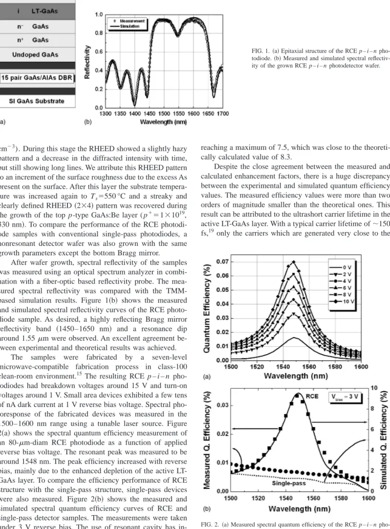
The optical design of the photodiode wafer was accom-plished by using transfer matrix method共TMM兲 based theo-retical simulations. Spectral reflectivity and responsivity simulations were carried out to find the desired epitaxial structure. The RCE p – i – n photodiode was designed to achieve a resonance at 1.55 m. In order to meet this reso-nance condition, a highly reflecting 15 pair GaAs/AlAs Bragg mirror centered at 1.55m was designed as the bot-tom mirror of the detector cavity. The air/GaAs interface acted as the top mirror for the resonant cavity. The cavity layers in between were formed by GaAs layers. To eliminate the standing wave effect in the resonant cavity, thickness of the active LT-GaAs layer was designed as an integer multiple of/2.13Except for the lightly absorptive LT-GaAs layer, all layers were transparent around the operation wavelength of 1.55 m. A schematic of the designed RCE photodiode structure is shown in Fig. 1共a兲.
Samples were grown on 3 in. semi-insulating GaAs wa-fers 共001兲 by molecular beam epitaxy. After thermal oxide desorption, a 0.15 m GaAs buffer layer was grown before the bottom GaAs/AlAs Bragg reflector. The reflector con-sisted of 15 pairs of undoped GaAs 共113.6 nm兲 and AlAs
共134.3 nm兲 layers grown with a substrate temperature
Ts⫽600 °C. On top of the reflector an undoped GaAs layer
共300 nm兲 was grown at Ts⫽550 °C and two n-type GaAs:Si
layers with n⫹⫽2⫻1018 cm⫺3 共300 nm兲 and n⫺⫽1
⫻1016 cm⫺3 共300 nm兲 were grown at the same substrate temperature. As4 flux was kept at 1⫻10⫺5 mbar during all the growth (As4/Ga flux ratio around 25兲. Reflection high-energy electron diffraction 共RHEED兲 pattern was streaky along the growth of the mirror. The substrate temperature was decreased to 200 °C for the growth of the 500-nm-thick lightly doped LT section of the detector (n⫺⫽1⫻1016 a兲Electronic mail: [email protected]
APPLIED PHYSICS LETTERS VOLUME 84, NUMBER 21 24 MAY 2004
4185
cm⫺3). During this stage the RHEED showed a slightly hazy pattern and a decrease in the diffracted intensity with time, but still showing long lines. We attribute this RHEED pattern to an increment of the surface roughness due to the excess As present on the surface. After this layer the substrate tempera-ture was increased again to Ts⫽550 °C and a streaky and
clearly defined RHEED共2⫻4兲 pattern was recovered during the growth of the top p-type GaAs:Be layer ( p⫹⫽1⫻1019, 330 nm兲. To compare the performance of the RCE photodi-ode samples with conventional single-pass photodiphotodi-odes, a nonresonant detector wafer was also grown with the same growth parameters except the bottom Bragg mirror.
After wafer growth, spectral reflectivity of the samples was measured using an optical spectrum analyzer in combi-nation with a fiber-optic based reflectivity probe. The mea-sured spectral reflectivity was compared with the TMM-based simulation results. Figure 1共b兲 shows the measured and simulated spectral reflectivity curves of the RCE photo-diode sample. As desired, a highly reflecting Bragg mirror reflectivity band 共1450–1650 nm兲 and a resonance dip around 1.55m were observed. An excellent agreement be-tween experimental and theoretical results was achieved.
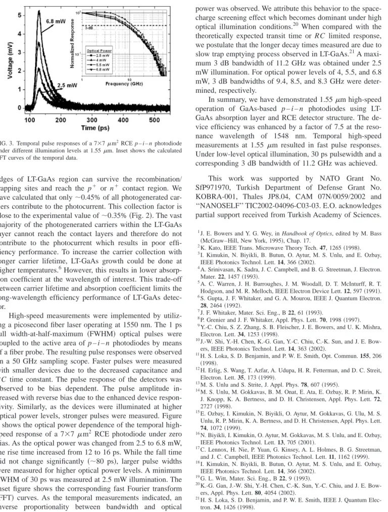
The samples were fabricated by a seven-level microwave-compatible fabrication process in class-100 clean-room environment.15The resulting RCE p – i – n pho-todiodes had breakdown voltages around 15 V and turn-on voltages around 1 V. Small area devices exhibited a few tens of nA dark current at 1 V reverse bias voltage. Spectral pho-toresponse of the fabricated devices was measured in the 1500–1600 nm range using a tunable laser source. Figure 2共a兲 shows the spectral quantum efficiency measurement of an 80-m-diam RCE photodiode as a function of applied reverse bias voltage. The resonant peak was measured to be around 1548 nm. The peak efficiency increased with reverse bias, mainly due to the enhanced depletion of the active LT-GaAs layer. To compare the efficiency performance of RCE structure with the single-pass structure, single-pass devices were also measured. Figure 2共b兲 shows the measured and simulated spectral quantum efficiency curves of RCE and single-pass detector samples. The measurements were taken under 3 V reverse bias. The use of resonant cavity has in-creased the quantum efficiency by a factor of 4.9. The mea-sured enhancement factor was even higher under zero bias
reaching a maximum of 7.5, which was close to the theoreti-cally calculated value of 8.3.
Despite the close agreement between the measured and calculated enhancement factors, there is a huge discrepancy between the experimental and simulated quantum efficiency values. The measured efficiency values were more than two orders of magnitude smaller than the theoretical ones. This result can be attributed to the ultrashort carrier lifetime in the active LT-GaAs layer. With a typical carrier lifetime of⬃150 fs,19 only the carriers which are generated very close to the
FIG. 1.共a兲 Epitaxial structure of the RCE p – i – n pho-todiode.共b兲 Measured and simulated spectral reflectiv-ity of the grown RCE p – i – n photodetector wafer.
FIG. 2. 共a兲 Measured spectral quantum efficiency of the RCE p – i – n pho-todiode as a function of applied reverse bias voltage.共b兲 Measured 共scatters兲 and simulated共solid and dotted lines兲 quantum efficiency curves for RCE and single-pass detector samples.
edges of LT-GaAs region can survive the recombination/ trapping sites and reach the p⫹ or n⫹ contact region. We have calculated that only⬃0.45% of all photogenerated car-riers contribute to the photocurrent. This collection factor is close to the experimental value of⬃0.35% 共Fig. 2兲. The vast majority of the photogenerated carriers within the LT-GaAs layer cannot reach the contact layers and therefore do not contribute to the photocurrent which results in poor effi-ciency performance. To increase the carrier collection with longer carrier lifetime, LT-GaAs growth could be done at higher temperatures.6However, this results in lower absorp-tion coefficient at the wavelength of interest. This trade-off between carrier lifetime and absorption coefficient limits the long-wavelength efficiency performance of LT-GaAs detec-tor.
High-speed measurements were implemented by utiliz-ing a picosecond fiber laser operatutiliz-ing at 1550 nm. The 1 ps full width-at-half-maximum 共FWHM兲 optical pulses were coupled to the active area of p – i – n photodiodes by means of a fiber probe. The resulting pulse responses were observed on a 50 GHz sampling scope. Faster pulses were measured with smaller devices due to the decreased capacitance and
RC time constant. The pulse response of the detectors was
observed to be bias dependent. The pulse amplitude in-creased with reverse bias due to the enhanced device respon-sivity. Similarly, as the devices were illuminated at higher optical power levels, stronger pulses were measured. Figure 3 shows the optical power dependence of the temporal high-speed response of a 7⫻7m2 RCE photodiode under zero bias. As the optical power was changed from 2.5 to 6.8 mW, the rise time increased from 12 to 16 ps. While the fall time did not change significantly 共⬃80 ps兲, larger pulse widths were measured for higher optical power levels. A minimum FWHM of 30 ps was measured at 2.5 mW illumination. The inset figure shows the corresponding fast Fourier transform
共FFT兲 curves. As the temporal measurements indicated, an
inverse proportionality between bandwidth and optical
power was observed. We attribute this behavior to the space-charge screening effect which becomes dominant under high optical illumination conditions.20 When compared with the theoretically expected transit time or RC limited response, we postulate that the longer decay times measured are due to slow trap emptying process observed in LT-GaAs.21A maxi-mum 3 dB bandwidth of 11.2 GHz was obtained under 2.5 mW illumination. For optical power levels of 4, 5.5, and 6.8 mW, 3 dB bandwidths of 9.4, 8.5, and 8.3 GHz were deter-mined, respectively.
In summary, we have demonstrated 1.55m high-speed operation of GaAs-based p – i – n photodiodes using LT-GaAs absorption layer and RCE detector structure. The de-vice efficiency was enhanced by a factor of 7.5 at the reso-nance wavelength of 1548 nm. Temporal high-speed measurements at 1.55 m resulted in fast pulse responses. Under low-level optical illumination, 30 ps pulsewidth and a corresponding 3 dB bandwidth of 11.2 GHz was achieved.
This work was supported by NATO Grant No. SfP971970, Turkish Department of Defense Grant No. KOBRA-001, Thales JP8.04, CAM 07N/0059/2002 and ‘‘NANOSELF’’ TIC2002-04096-C03-03. E.O. acknowledges partial support received from Turkish Academy of Sciences. 1J. E. Bowers and Y. G. Wey, in Handbook of Optics, edited by M. Bass
共McGraw–Hill, New York, 1995兲, Chap. 17.
2K. Kato, IEEE Trans. Microwave Theory Tech. 47, 1265共1998兲. 3
I. Kimukin, N. Biyikli, B. Butun, O. Aytur, M. S. Unlu, and E. Ozbay, IEEE Photonics Technol. Lett. 14, 366共2002兲.
4A. Srinivasan, K. Sadra, J. C. Campbell, and B. G. Streetman, J. Electron.
Mater. 22, 1457共1993兲.
5A. C. Warren, J. H. Burroughes, J. M. Woodall, D. T. McInturff, R. T.
Hodgson, and M. R. Melloch, IEEE Electron Device Lett. 12, 597共1991兲.
6S. Gupta, J. F. Whitaker, and G. A. Mourou, IEEE J. Quantum Electron.
28, 2464共1992兲.
7J. F. Whitaker, Mater. Sci. Eng., B 22, 61共1993兲. 8
P. Grenier and J. F. Whitaker, Appl. Phys. Lett. 70, 1998共1997兲.
9
Y.-C. Chiu, S. Z. Zhang, S. B. Fleischer, J. E. Bowers, and U. K. Mishra, Electron. Lett. 34, 1253共1998兲.
10J.-W. Shi, Y.-H. Chen, K.-G. Gan, Y.-C. Chiu, C.-K. Sun, and J. E.
Bow-ers, IEEE Photonics Technol. Lett. 14, 363共2002兲.
11
H. S. Loka, S. D. Benjamin, and P. W. E. Smith, Opt. Commun. 155, 206
共1998兲.
12H. Erlig, S. Wang, T. Azfar, A. Udupa, H. R. Fetterman, and D. C. Streit,
Electron. Lett. 35, 173共1999兲.
13
M. S. Unlu and S. Strite, J. Appl. Phys. 78, 607共1995兲.
14
M. S. Unlu, M. Gokkavas, B. M. Onat, E. Ata, E. Ozbay, R. P. Mirin, K. J. Knopp, K. A. Bertness, and D. H. Christensen, Appl. Phys. Lett. 72, 2727共1998兲.
15E. Ozbay, I. Kimukin, N. Biyikli, O. Aytur, M. Gokkavas, G. Ulu, M. S.
Unlu, R. P. Mirin, K. A. Bertness, and D. H. Christensen, Appl. Phys. Lett.
74, 1072共1999兲.
16N. Biyikli, I. Kimukin, O. Aytur, M. Gokkavas, M. S. Unlu, and E. Ozbay,
IEEE Photonics Technol. Lett. 13, 705共2001兲.
17
C. Lennox, H. Nie, P. Yuan, G. Kinsey, A. L. Holmes, B. G. Streetman, and J. C. Campbell, IEEE Photonics Technol. Lett. 11, 1162共1999兲.
18I. Kimukin, N. Biyikli, B. Butun, O. Aytur, M. S. Unlu, and E. Ozbay,
IEEE Photonics Technol. Lett. 14, 366共2002兲.
19G. L. Witt, Mater. Sci. Eng., B 22, 9共1993兲. 20
K.-G. Gan, J.-W. Shi, Y.-H. Chen, C.-K. Sun, Y.-C. Chiu, and J. E. Bow-ers, Appl. Phys. Lett. 80, 4054共2002兲.
21H. S. Loka, S. D. Benjamin, and P. W. E. Smith, IEEE J. Quantum
Elec-tron. 34, 1426共1998兲. FIG. 3. Temporal pulse responses of a 7⫻7m2RCE p – i – n photodiode
under different illumination levels at 1.55m. Inset shows the calculated FFT curves of the temporal data.
4187