Counting Molecules with a Mobile Phone Camera Using Plasmonic
Enhancement
Sencer Ayas,
†Andi Cupallari,
†Okan Oner Ekiz,
†Yasin Kaya,
‡and Aykutlu Dana*
,††UNAM Institute of Materials Science and Nanotechnology and‡Department of Electrical and Electronics Engineering, Bilkent
University, 06800 Ankara, Turkey
*
S Supporting InformationABSTRACT: Plasmonicfield enhancement enables the acquisition of Raman spectra at a single molecule level. Here we investigate the detection of surface enhanced Raman signal using the unmodified image sensor of a smart phone, integrated onto a confocal Raman system. The sensitivity of a contemporary smart phone camera is compared to a photomultiplier and a cooled charge-coupled device. The camera displays a remarkably high sensitivity, enabling the observation of the weak unenhanced Raman scattering signal from a silicon surface, as well as from liquids, such as ethanol. Using high performance wide area plasmonic substrates that enhance the Raman signal 106to 107
times, blink events typically associated with single molecule motion, are observed on the smart phone camera. Raman spectra can also be collected on the smart phone by converting the camera into a low resolution spectrometer with the inclusion of a collimator and a dispersive optical element in front of the camera. In this way, spectral
content of the blink events can be observed on the plasmonic substrate, in real time, at 30 frames per second.
KEYWORDS: plasmonics, metamaterials, surface-enhanced Raman spectroscopy
S
urface-enhanced Raman spectroscopy (SERS) uses plas-monic structures to enhance the intensity of Raman spectra of submonolayer coverage molecularfilms to levels that allow single molecule sensitivity.1−7 Although it was originally accepted that extremely high enhancement factors of 109 to1012 was required for single molecule level SERS, later lower
enhancement factors (106 to 108) were observed to be
sufficient.8A variety of techniques are used to produce metallic nanoparticles or surface bound metallic structures which enable SERS. Recently, we used an engineered meta-surface with subwavelength periodicity to demonstrate high uniformity and high spatial resolution confocal SERS imaging.9A scaled down version of the substrates fabricated through conventional clean-room fabrication methods were used in stochastic SERS imaging to provide a resolution of 20 nm, using a low cost CMOS camera.10In this article, we investigate detection of the SERS signal from a confocal Raman microscope using the camera of an unmodified smart phone. Mobile phones are used influorescence microscopy and even in optofluidic applications such as cytometry.11−16 Recently, a smart phone was used for fluorescent detection of 90 nm sized labeled nanoparticles and viruses.17It is suggested that enhancement of thefluorescence and Raman signals may enable single molecule level sensing using a smart phone.18Here, we demonstrate label-free single molecule blink event detection on a smart phone, enabled by a plasmonic metasurface fabricated using dewetting of Ag on HfO2 deposited on an Ag underlayer by atomic layer deposition. Also, low resolution spectrometric detection of the unenhanced Raman signal is demonstrated by converting the smart phone to a spectrometer through the inclusion of a
dispersive optical element in the beam path. The plasmon enhanced Raman signal from individual blink events are shown to produce sufficient number of photons for spectroscopic detection of single molecule events.
The surface enhanced Raman Stokes signal can be estimated according to PSERS(ω
S) = Nσ|AE|2|AS|2IE, where IE is the
excitation laser intensity,σ is the Raman cross section of the adsorbed molecule, possibly increased due to chemical enhancement, N is the number of molecules involved in the SERS process, and AEand ASare thefield enhancement factors (for excitation frequency ωEand Raman scattering frequency
ωS).
19
The electromagnetic SERS enhancement factor is therefore roughly proportional to the fourth power of the field enhancement around the excitation and scattering wavelengths. Without plasmonic enhancement (i.e., AE = AS
= 1), the Raman signal is proportional to the excitation intensity IE and the total number of scattering molecules, N.
For bulk measurements in the confocal configuration, Raman scattering comes mainly from the material contained within the focal volume, corresponding to about 1010 molecules for diffraction limited focusing with a high numerical aperture objective. The Raman scattering cross sections are small, typically ∼10−30 to 10−24 cm2 per molecule, and the Raman
scattering signal can amount to 100−1000 photons per second using 10 mW excitation in the visible region. Plasmonic structures can enhance the signal significantly, thereby increasing the signal from single or few molecules to levels
Received: November 7, 2013 Published: December 26, 2013
that can be detected using a cooled CCD spectrometer or a photomultiplier. Cooled detectors are bulky and have higher power consumption and are therefore not preferable for mobile platforms. Plasmonic enhancement can eliminate the need for cooling, and determining the conditions for sufficient enhance-ment of the Raman signal is important for evaluation of the potential use of uncooled detectors for capturing Raman spectra. Contemporary portable phones are typically equipped with miniature cameras, with relatively small input aperture diameters on the order of millimeters. The cameras are mostly able to capture video at 30 frames per second (fps) and are designed to capture low noise images, even in poor lighting conditions. Typically the cameras are fabricated using silicon, and intrinsic quantum efficiency of silicon photodiodes can reach 60−80%. Color filters enable red, green, and blue channels to be detected separately, resulting in color images accompanied by a potential decrease in external quantum efficiency. Electronic circuitry that is used in the acquisition of the photodiode signal may have automatic gain control, which allows operation under low light level conditions. The pixel count, uniformity, sensitivity, and noise level of the cameras have steadily improved.
A key requirement in single molecule fluorescence imaging or Raman spectroscopy is a sensor with a large enough minimum detectable power level that would produce a signal for a given influx of photons from a weak source. In order to compare the sensitivity of a smart phone camera with a photomultiplier and a cooled CCD, we use the setup shown in Figure 1a (also see Figure S1). The setup is based on a commercial confocal Raman microscope, slightly modified to accommodate the smart phone camera to record wide-field Raman images. We record the Raman spectrum of a silicon
substrate, using 10 mW, 532 nm excitation. Laser is focused to a diffraction limited spot using a 0.9 NA, 100× objective. The Raman spectrum is recorded using a cooled linear charge coupled device (CCD) and is shown in Figure 1b. The optical signal can be routed by a switch to the imaging path, where an eyepiece is used to focus the light onto the smart phone camera. The inset of Figure 1b shows the green pixel counts extracted from a 30 fps video capture of the Raman scattering signal. The pixel size is calibrated by imaging a mask of known dimensions and is 480 nm. Poor focusing optics result in a broadened spot diameter of 1.4μm. Although the measurement is done using a nonportable microscope, in principle the setup can easily be miniaturized. The Raman signal is also recorded using a photomultiplier and relative counts are shown in Figure 1c. The red, green, and blue (R, G, and B)filters of the smart phone sensor are nonideal, and overlapping transmittance results in 550 nm green light to be recorded in the blue and red channels as well (Figure 1c inset). It should be noted that color filters present on the sensor potentially degrades the resolution, and no effort was made to enhance the resolution by manipulating the demosaiced images from the camera. In order to make better use of the scarce photons, R, G, and B values are simply added. The relative sensitivity of the smart phone camera is measured by changing the excitation power and measuring camera output versus photomultiplier count rate (Figure 1d). The minimum detectable signal at 30 fps can be inferred from the intercept of the line in Figure 1e and is equivalent to 104counts per second (cps). Noise plays a central
role in determining the signal-to-noise ratio in any type of sensing, particularly important for blinking event detection. Noise level and signal stability of the smart phone camera is also measured using wide field illumination by a white LED
Figure 1.(a) Schematic description of the measurement setup. (b) Raman spectrum of silicon acquired using 10 mW of excitation power at 532 nm, focused to a diffraction limited spot, collected by a 100 μm core diameter fiber. Inset shows the green channel intensity from a capture of the spot using the smart phone camera at 30 frames per second (fps); pixel size is 480 nm. (c) Relative photon count rate (counts per second, cps) for a photomultiplier, a cooled linear CCD and the smart phone at 30 fps. (d) The pixel intensity of the smart phone camera vs photomultiplier count rate shows linearity of the camera output. The minimum detectable count rate is inferred by the intercept, at 10 Kcps, (e) Time series of the camera output for a single pixel when illuminated by a white light LED shows a peak to peak noise of 5 counts. The inset shows the histogram of pixel intensity, showing a distribution with width 2σ = 2.2 counts. (f) Power spectral density for the intensity of a single pixel, calculated by taking the Fourier transform of time series, shows slightly increased noise at low frequencies.
source dimmed down to produce∼100 counts/pixel/frame at 30 fps (Figure 1e). Peak to peak value of the pixel intensity noise is∼5 counts at 30 fps. A pixel value histogram is shown in the inset of Figure 1e. Noise spectrum is calculated using
Fast-Fourier Transform and shows a slight increase at lower frequencies (Figure 1f). In the image snapshot mode, it is observed that the camera can capture clear images of the Raman signal even at low PMT count rates (as low as 10 Kcps),
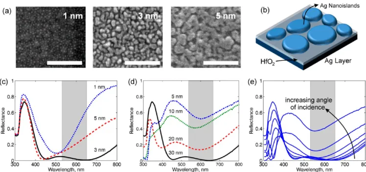
Figure 2.(a) Scanning electron micrographs (SEM) of plasmonic surfaces with 1, 3, and 5 nm mass thickness Ag overlayer shows coarsening and percolation of Ag nanoislands. Scale bars 250 nm. Plasmonicfield enhancement is greater as the nanoislands approach each other, reducing the interparticle gap. Mass thickness sample of 3 nm exhibits greatest hot spot density. (b) Schematic view of the substrate showing layer structure. (c) Reflectance of the surfaces near normal incidence for 1, 3, and 5 nm mass thickness Ag overlayer and 30 nm HfO2. Gray band shows the wavelength
region of interest for Raman scattering excited by 532 nm light. Ag mass thickness of 3 nm results in a wide band metasurface. (d) The reflectance is plotted for HfO2thicknesses of 5, 10, 20, and 30 nm. (e) Dependence of reflectance on angle of incidence is plotted for 20, 30, 40, 50, 60, 70, and
80°. The 30 nm HfO2/ 3 nm Ag surface is quasi-omnidirectional, maintaining high absorption over a wide wavelength range at angles up to 60°.
Figure 3.(a) Maximum|E|2field enhancement factor as a function of wavelength, plotted for 10, 20, and 30 nm dielectric thickness for a periodic
arrangement of Ag nanoislands (40 nm period, 10 nm thickness, 35 nm island size, 75° sidewall angle), shows an increase in the enhancement around 550 nm as thickness increases to 30 nm. (b) Calculated reflectance of the periodic arrangement, plotted as a function of wavelength. (c) Maximum|E|2field enhancement factor as a function of wavelength, for a quasi-random surface derived from SEM data as a function of dielectric
thickness. (d) Calculated reflectance of the quasi-random arrangement, plotted as a function of wavelength and dielectric thickness. A dielectric thickness of 40 nm is also included in the calculations, as it betterfits the experimental reflectance for 30 nm HfO2shown in Figure 2e.
with high signal-to-noise ratio. Since the camera does not allow setting the integration time in snapshot mode, we do not attempt to quantify the absolute sensitivity in snapshot mode. We use an improved version of the plasmonic metasurface substrate described in our earlier work.10Substrates fabricated by dewetting of silver films were studied before for their plasmonic properties and SERS enhancement.20,21Metals near percolation threshold have localized surface plasmon resonance due to their nanoparticle nature. By changing fabrication conditions, resonances of the surface can be tuned. Placing metal nanoparticles over a metal surface, with an insulator separator in between, results in strong changes in overall plasmonic properties due to the interaction of metal nano-particle with the metalfilm.22−25It is seen that Ag nanoislands form at a mass thickness of 1 nm, coarsening takes place at 3 nm, and percolation begins at 5 nm mass thickness (Figure 2a). For 3 nm top metal mass thickness, the gap between individual nanoparticles is about 5−10 nm and nanoisland thickness is 10 nm on the average. HfO2thickness of 30 nm and Ag nanoisland
layer mass thickness of 3 nm produces a wide band perfect absorber as measured by spectroscopic ellipsometry (Figure 2c,d). The metasurfaces are quasi-omnidirectional and absorption is above 90% for the 30 nm thick HfO2 sample
over a wavelength range of 450 to 800 nm, for angle of incidence of up to 60° (Figure 2e). Electromagnetic properties are calculated for periodic nanoislands with 75° sidewall angles (Figure 3a,b), as well as for SEM data based model surfaces (Figure 3c,d, also see Figures S2 and S3) using computational tools. The peak SERS enhancement factor around 550 nm is estimated to be between 106to 2× 10⁷. The surfaces exhibit a large density of hot spots which display blinking Raman signals when viewed using wide field laser illumination. Plasmonic metamaterial surfaces have been demonstrated to have broadband absorption and superior field enhancements that are fabricated using electron beam lithography.26 In contrast, the surfaces presented here require no lithography, hence, are easy to fabricate over large areas. The resonance wavelengths can be tuned by changing the thickness of spacer layer and by control of island diameter and thickness. Optimized surfaces with 30 nm HfO2 dielectric thickness and 10 nm island
thickness have broadband plasmon resonances over the whole visible spectrum with almost 90% average absorption. The broadband absorption is due to both the interparticle and the particle−metal film couplings. Mode confinements are shown for a periodic nanoisland arrangement, as shown in Figure 4. Interparticle coupling is attributed to a dipolar coupling between individual nanoparticles, which is known as electrical resonance where magnetic field is confined between the nanoparticles (Figure 4a). The particle−metal film coupling, typically referred to as the magnetic resonance, has the magnetic field confined to the spacer layer (Figure 4b).27 A coupling of the two types of resonances is also present and enhances the absorption in the intermediate wavelength region between the two resonances. The thickness of the Ag islands are important for having an optimal enhancement (Figure 4c,d). For single molecule SERS enhancement, the surfaces need to be optimized, and optimal SERS enhancement is achieved when plasmonic resonances cover the range of excitation and scattering frequencies.28 We optimized the SERS enhancement at excitation and scattering wavelengths (532−650 nm wavelength range, corresponding to Raman range of 0−3500 cm−1) by sweeping the fabrication parameters. The dielectric layer is very important in achieving the
enhancement levels presented here and provides about an order of magnitude improvement. This effect is studied recently by independent groups, using SiO2as the spacer.29
To characterize the spectral content of the blink events, we record the time-dependent Raman spectra on a bright hot spot, using a cooled CCD spectrometer, as shown in Figure 5. The integrated intensity between 0 and 3500 cm−1 is plotted as a function of time in Figure 5a. The integration time of the spectrometer is 100 ms. Sudden changes in the spectrum are observed as peaks in the time series. The spectra show distinct Raman bands that fluctuate in both intensity and frequency, which is commonly interpreted as a positive indication for single molecule level sensitivity (Figure 5b). The debate about the interpretation offluctuating Raman bands as evidence for single molecule SERS is ongoing in the literature.30−35 It is claimed that thermally activated diffusion and Brownian motion of molecules are possibly responsible for the observed SERS signals.18,36−38 Fluctuations of intensity of optical emission from silver nanoparticles were claimed to be independent of the intentional presence of probe molecules but an inherent feature related to Ag nanoparticles.39 However, we note that in our experiments, when untreated surfaces are subjected to airborne molecules, for example by spraying a mixture of carbon compounds from a fragrance bottle, a sudden increase of blinking is observed (see Supporting Information, Video 1, captured using a monochrome CMOS camera). Diffusion of large molecules on metal surfaces has been directly observed and characterized using scanning tunneling microscopy.40−42 Also, spurious lines are routinely present in blinking SERS spectra.43Based on such previous observations, we attribute the unidentified spectra to the presence of adsorbed volatile organic compounds present in ambient air.44,45 It is observed that the plasmonic substrates also enhance thefluorescence signal, and once in a while a broadfluorescence spectrum is captured as shown in Figure 5c. Such enhancements of the fluorescence were previously studied using plasmonic antennae.46 The optical spectrum during most blink events exhibit Raman bands, shown in Figure 5d, typically superimposed on a broad fluorescence background from the Ag nanoisland layer. In comparison, no signal can be observed on aflat Ag surface.
Figure 4. (a) Cross sectional magnetic field profile for a periodic arrangement of metal−insulator−metal resonators (40 nm period, 35 nm width, 20 nm thickness, 75° sidewall angle Ag, on 20 nm HfO2, on
Ag) at 430 nm excitation wavelength and (b) at 700 nm excitation wavelength. (c) For a top metal thickness of 10 nm, fields have enhancement at the top surface (excited at 550 nm) as compared to (d) a top metal thickness of 20 nm (all scale bars are 20 nm wide).
The blinks are captured using the smart phone camera at 30 fps, and are shown in Figure 6a (also see Supporting Information, Video 2). The relative enhancement of the substrates as a function of dielectric thickness and Ag overlayer thickness can be seen in the increase offluorescence signal from the Ag nanoisland layer. A dielectric thickness of 30 nm and an Ag overlayer mass thickness of 3 nm produces the highest blink rate with high blink intensities, an observation that correlates well with the reflection spectra of the surfaces. The blinks are counted using QuickPalm and histograms are generated as shown in Figure 6b.47 The pixel noise superimposed on the fluorescence background causes the QuickPalm algorithm to detect erroneous blink events with low peak intensity, causing an increased blink count at low intensities.
Simple detection of blink events using the smart phone camera is interesting, however, it is highly desirable to actually record the spectral content of the Raman scattering signal. In order to demonstrate that the smart phone can be used as a spectrometer, we use the setup shown in Figure 7a. The collection fiber output is collimated using a lens and a transmission grating is positioned before the focusing lens of
the camera. In this configuration (smart phone spectrometer configuration), wavelength separation of the light can be achieved with reasonable linearity (see Figures S4 and S5). A similar configuration has been recently used to record the spectra of a white light source and perform label-free biomolecular detection.48The wavelength dependent response is not uniform due to the colorfilters on the camera, however we do not attempt spectral equalization and use the data as it is extracted from the snapshots and video captures. We record the unenhanced Raman spectrum of silicon and ethanol on silicon using the cooled CCD spectrometer as shown in Figure 7b and compare the results with the smartphone-spectrometer data shown in Figure 7c. A 300 lines per mm (lpmm) transmission grating allows observation on zeroth, first, and second order diffraction orders, as shown in the insets. A close-up of the second order region is shown in Figure 7d, superimposed with the original Raman spectra shown in Figure 7b, convolved with a point spread function of the smartphone-spectrometer. The resolution (>180 cm−1for 532 nm excitation) is limited by the diffractive power of the grating as well as the diameter of the fiber (25 μm diameter) and focal length of the collimator
Figure 5.(a) Time series of the integrated intensity within 0 to 3500 cm−1, as recorded by the cooled CCD spectrometer on a particularly bright hot-spot, shows blinking events asfluctuations in the intensity (500 μW of excitation at 532 nm). (b) The time series plotted to feature the full spectrum exhibits Raman lines thatfluctuate in intensity and frequency, characteristic of single molecule SERS. (c) Occasionally, a fluorescent molecule is captured in the hot-spot (at time 35 s in (a)). (d) Typical Raman spectra during a SERS blink (at time 76 s in (a)) exhibits a broad fluorescence superimposed with distinct Raman bands.
(10.99 mm, F220-SMA-B Thorlabs). The fluctuating Raman spectra can be recorded using the SERS substrate, as shown in Figure 8a, where multiple snapshots are recorded consecutively, using a 600 lpmm grating, with an integration time on the order
of 1 s. Distinct spectral features can be observed during blink events. The spectral features can still be observed at 30 fps, as shown in Figure 8b (also see Supporting Information, Video 3). In order to demonstrate the superior signal intensity of SERS,
Figure 6.(a) Frames from video captures using the smart phone camera on plasmonic surfaces with 1, 3, and 5 nm mass thickness Ag overlayer and 5, 10, 20, 30 nm HfO2dielectric layer thickness. Excitation laser is defocused to illuminate an area 50μm in diameter. Arrows denote blink events on
afluorescence background of the Ag nanoisland layer (also see Supporting Information, Video). Scale bar is 20 μm wide. (b) Video frames are analyzed to extract a histogram of blink event intensity for the 3 nm Ag samples at varying HfO2thickness. A dielectric thickness of 30 nm produces
brightest blink events. As the bottom Ag layer is removed (dielectric thickness infinite), blink events can still be observed, however at a decreased rate and intensity. Inset shows the potential source of blinking, i.e., surface diffusion of physisorbed volalite organic compounds into and out of hot spots.
Figure 7.(a) Configuration for using the smart phone camera as a low resolution spectrometer. The collection fiber from the Raman setup is collimated and dispersed with a transmission grating (300 lines per mm) before entering the camera. (b) Raman spectra of silicon and ethanol on silicon collected with 13 mW of 532 nm excitation using the cooled CCD spectrometer are shown. (c) Smart phone camera recordings of the two orders of the dispersed input light in the snapshot mode. Solid blue lines show integrated pixel intensity and dotted red line shows superimposed Raman spectra convolved with a line shape function that represents the point spread function (PSF) of the optical configuration. Insets show actual camera excerpts. (d) Close-up of the second order diffraction region of the camera output (solid lines) superimposed with Raman spectra shown in (b) convolved with the PSF of the configuration.
we record the Raman spectra on plasmonic substrates treated with 10 nM methylene blue solution and 1 μM cresyl violet solution in using 100μW excitation (Figure 8c,d). Correspond-ing spectra are also captured usCorrespond-ing the smart phone camera as shown in Figure 8e,f. Although thefluctuating spectra contain signatures that can be attributed to cresyl violet and methylene blue, spurious signals are also present that show presence of unidentified molecules occasionally producing Raman bands. As SERS spectra are typically modified as compared to bulk spectra, we do not attempt to identify the spurious molecules.
In summary, we demonstrate that using substantial plasmonic enhancement, single molecule events can be detected through SERS, using the camera of a contemporary smart phone at 30fps. The video captures can be analyzed to distinguish individual blink events. Even weaker optical signals (10 Kcps) can be observed on the smart phone camera in snapshot mode with high signal-to-noise ratio, which we are unable to further quantify because of lack of knowledge about the integration time. The smart phone can be used as a spectrometer using a collimator and a transmission grating,
Figure 8.(a) False color coded excerpts from series of smart phone camera snapshot captures during blink events on the plasmonic substrate, in the spectrometer configuration (1 mW excitation at 532 nm). The spectral region is cropped, rotated and stitched for each frame. Inset shows actual camera color coding of the same data. Integration time per frame is∼1 s. (b) False color coded excerpts from a video sequence recorded at 30 frames per second. Although video recording is at lower resolution, distinct spectral features during blink events can be observed (also see Supporting Information, Video). The SERS spectra of plasmonic surfaces (30 nm HfO2thickness) were also recorded using the cooled CCD spectrometer,
treated with 10 nM methylene blue solution in (c) and 1μM cresyl violet solution in (d) using 100 μW excitation. Corresponding spectra are also captured using the smart phone camera as shown in (e) and (f). Insets show excerpts of the region of interest from actual camera captures in snapshot mode.
which with the enhancement of the plasmonic substrate is able to observe the spectral content of single blink events. Although the experiments were performed on a nonportable microscope system, the setup does not differ from a fluorescence measurement setup and can be potentially miniaturized. Use of low excitation powers (0.1−10 mW) also favors the potential for miniutarization. It must be noted that, although electro-magnetic calculations estimate an overall enhancement factor of about 107, the large intensity of the blinking signals suggest that
the chemical or first layer contribution to SERS is not negligible. Such chemical enhancement can be significant, up to 2 orders of magnitude chemical enhancement due to complex mechanisms leading to charge transfer between the metal and the probe molecule has been predicted.49Therefore, the SERS spectra differ significantly from unenhanced Raman spectra, and should be understood beyond simpler electro-magnetic models. On the other hand, SERS spectra are repeatable in themselves, and the plasmonic substrates that enable the observations can be fabricated on large area substrates without the need for top-down patterning, therefore can be produced at low cost. The width of the spectra acquired using a 600 lpmm grating is about 1/8th of the overallfield of view. In principle, by using a grating with higher groove density, the dispersion can be increased and resolution of the spectrometer configuration can be improved to better allow discrimination of spectra. However, for using the fullfield of view of the camera, additional optics may be required to improve the resolution to about 20 cm−1. The remarkable sensitivity of the smart phone camera combined with high plasmonic enhancement of the optical signal as demonstrated in this article, may pave the way for low cost hand-held systems which can be used in the analytical study of samples at a single molecule level.
■
METHODSSample Preparation and Characterization. Germanium (2−3 nm, 99.99% purity) is deposited on silicon (100) substrates using an e-beam evaporation system (Vaksis PVD Vapor 4S e-beam) as wetting and adhesion layer with a deposition rate 0.5 Å/s. Then 50 nm thick Ag layer (99.99% purity) is deposited with the e-beam evaporation system, with a deposition rate of 0.6−0.8 Å/s. For the dielectric spacer layer, 5−30 nm HfO2is deposited by atomic layer deposition. For the
nanoisland layer, 1−5 nm Ag (99.99% purity) is deposited using the e-beam evaporation system with a deposition rate of 0.6−0.8 Å/s. Spectrosopic ellipsometry was used to characterize the thickness of HfO2films and final plasmonic surfaces, and
were performed on a J.A.Woolam V-VASE ellipsometer. Reflections of the fabricated plasmonic surfaces are also characterized by custom built reflection setup for normal incidence. In the custom built setup, white light is coupled to a 400μm core multimode fiber. Light output is then collimated using a lens. Using a beam splitter light is sent on the sample and the reflected light is coupled to another 400 μm core multimode fiber with a lens through the beam splitter. The collected light is sent to a UV−vis spectrometer (from Ocean Optics). As a reference mirror, a 2× 2 cm2Ag coated silicon (80 nm thickness) is used in the 400−800 nm range.
Raman Measurements. Raman measurements were performed on a WITEC confocal Raman microscope equipped with 532 nm excitation source. The smart phone was attached to a holder and placed in front of the camera output of the system, where the camera was replaced with a 10× eyepiece.
Spectrometer configuration was achieved by using a collimator (10.99 mm focal length, F220-SMA-B Thorlabs) and a 25μm diameter collectionfiber, collimating the Raman signal from the confocal microscope. Blazed transmission gratings (300 and 600 lpmm from Thorlabs, GT50−03 and GT50−06) were used in front of the phone camera lens for dispersion. For unenhanced bulk Raman measurements, bare silicon was covered with a drop of ethanol and a 150 μm thick cover slide was used to prevent evaporation as well as to maintain planarity. For plasmon enhanced spectra acquisition, the plasmonic surfaces were immersed in 1 μM of cresyl violet solution in ethanol and 10 nM of methylene blue solution in deionized water for extended periods (>30 min) and dried with nitrogen.
Simulations. Simulations are done with a commercial FDTD package (Lumerical). For the magneticfield profiles in Figure 3, each nanoparticle assumed as truncated cone with 35 nm radius and 75 slanted angle and 10−20 nm heights. Symmetric and antisymmetric boundary conditions are used along x and y axes to reduce the computational cost. Perfectly matched layer (PML) boundary condition is used in the z axis. Period of the simulation domain 40 nm for both x and y axes. A broadband plane wave (200−1000 nm) is used to calculate the reflection spectrum and magnetic field profiles. The mesh size is used in the simulations are 1× 1 × 1 nm3except the volume
containing nanoparticle and spacer layer where 0.25× 0.25 × 0.25 nm3mesh size is used. Dielectric function of silver used in the simulations is from the program database. Dielectric function of silver isfitted to polynomial with 10−5fit tolerance, 12 coefficients, and 12 imaginary weight using program’s fitting algorithm. Germanium wetting layer is neglected in the simulations. The experimental obtained dielectric function of HfO2is used and it isfitted to 12 order polynomial with 10−5fit
tolerance and 5 imaginary weight is used. Field enhancement is calculated using the maximum field intensity enhancement factor on the nanoparticle. Computational Raman enhance-ment factor is calculated using the|E(λ)|4factor, whereλ = 532 nm. SEM image of nanoparticle films (collected on an FEI environmental SEM system) are imported to the FDTD program. Bloch periodic condition is used for both x and y axes. Period is 300 nm for both x and y axes. Thickness of top metallicfilm is 10 nm. Field profiles for 532 nm wavelength is obtained at nanoparticle film HfO2 interface in the middle
plane of nanoparticlefilm and at the top of nanoparticle film.
■
ASSOCIATED CONTENT*
S Supporting InformationSupplementary Figures: Figure S1, annotated photograph of the measurement setup in the imaging configuration; Figures S2 and S3, electromagnetic simulation results of a model surface derived from scanning electron micrographs of the plasmonic surface; Figure S4, annotated photograph of the measurement setup for spectroscopy configuration; Figure S5, wavelength dependent capture of light with the smartphone in the spectrometer configuration. Supplementary Video captures: Video 1, the effect of airborne molecules on the blink events; Video 2, video capture of blink events using the smartphone; Video 3, spectral video capture during blinks events. This material is available free of charge via the Internet at http:// pubs.acs.org.
■
AUTHOR INFORMATION Corresponding Author*E-mail: [email protected].
Notes
The authors declare no competingfinancial interest.
■
ACKNOWLEDGMENTSThis work was partially supported by TUBITAK under Grant 111M344, EU FP7:People-IAPP NanoBacterPhageSERS.
■
REFERENCES(1) Jeanmaire, D. L.; Duyne, V. R. P. Surface Raman spectroelec-trochemistry: Part I. Heterocyclic, aromatic, and aliphatic amines adsorbed on the anodized silver electrode. J. Electroanal. Chem. 1997, 84, 1−20.
(2) Albrecht, M. G.; Creighton, J. A. Anomalously intense Raman spectra of pyridine at a silver electrode. J. Am. Chem. Soc. 1997,99, 5215−5217.
(3) Stiles, P. L.; Dieringer, J. A.; Shah, N. C.; Duyne V., R. P. Surface-enhanced raman spectroscopy. Annu. Rev. Anal. Chem. 2009, 1, 601− 626.
(4) Nie, S.; Emory, S. R. Probing single molecules and single nanoparticles by surface-enhanced raman scattering. Science 1997, 275, 1102−1106.
(5) Kneipp, K.; Wang, Y.; Kneipp, H.; Perelman, L. T.; Itzkan, I.; Dasari, R. R.; Feld, M. S. Single molecule detection using surface-enhanced raman scattering (SERS). Phys. Rev. Lett. 1997, 78, 1667− 1670.
(6) Kneipp, K.; Wang, Y.; Dasari, R. R.; Feld, M. S. Approach to single molecule detection using surface-enhanced resonance Raman scattering (SERRS): A study using rhodamine 6G on colloidal silver. Appl. Spectrosc. 1995, 49, 780−784.
(7) Kneipp, K.; Kneipp, H.; Manoharan, R.; Itzkan, I.; Dasari, R. R.; Feld, M. S. Surface-enhanced Raman scattering (SERS): A new tool for single molecule detection and identification. Bioimaging 1998,6, 104−110.
(8) Ru, E. C. L.; Etchegoin, P. G. Single-molecule surface-enhanced raman spectroscopy. Annu. Rev. Phys. Chem. 2012,63, 65−87.
(9) Ayas, S.; Güner, H.; Türker, B.; Ekiz, O. O.; Dirisaglik, F.; Okyay, A. K.; Dâna, A. Raman enhancement on a broadband meta-surface. ACS Nano 2012, 6, 6852−6861.
(10) Ayas, S.; Cinar, G.; Ozkan, A. D.; Soran, Z.; Ekiz, O.; Kocaay, D.; Tomak, A.; Toren, P.; Kaya, Y.; Tunc, I.; Zareie, H.; Tekinay, T.; Tekinay, A. B.; Guler, M. O.; Dana, A. Label-free nanometer-resolution imaging of biological architectures through surface enhanced raman scattering. Sci. Rep. 2013, 3, 2624.
(11) Zhu, H.; Yaglidere, O.; Su, T.-W.; Tseng, D.; Ozcan, A. Cost-effective and compact wide-field fluorescent imaging on a cell phone. Lab Chip 2011, 11, 315−322.
(12) Zhu, H.; Mavandadi, S.; Coskun, A. F.; Yaglidere, O.; Ozcan, A. Optofluidic fluorescent imaging cytometry on a cell phone. Anal. Chem. 2011, 83, 6641−6647.
(13) Smith, Z. J; Chu, K.; Espenson, A. R.; Rahimzadeh, M.; Gryshuk, A.; Molinaro, M.; Dwyre, D. M.; Lane, S.; Matthews, D.; Wachsmann-Hogiu, S. Cell-phone-based platform for biomedical device development and education applications. PLoS ONE 2011, 6 (3), e17150.
(14) Breslauer, D. N.; Maamari, R. N.; Switz, N. A.; Lam, W. A.; Fletcher, D. A. Mobile phone based clinical microscopy for global health applications. PLoS ONE 2009, 4 (7), e6320.
(15) Tseng, D.; Mudanyali, O.; Oztoprak, C.; Isikman, S.; Sencan, I.; Yaglidere, O.; Ozcan, A. Lens-free microscopy on a cell phone. Lab Chip 2010, 10, 1787−1792.
(16) Zhu, H.; Sikora, U.; Ozcan, A. Quantum dot enabled detection of Escherichia coli using a cell-phone. Analyst 2012, 137 (11), 2541−4. (17) Wei, Q.; Qi, H.; Luo, W.; Tseng, D.; Ki, S. J.; Wan, Z.; Göröcs, Z.; Bentolila, L. A.; Wu, T.-T.; Sun, R.; Ozcan, A. Fluorescent imaging
of single nanoparticles and viruses on a smart phone. ACS Nano 2013, 7 (10), 9147−9155.
(18) Khatua, S.; Orrit, M. Toward single-molecule microscopy on a smart phone. ACS Nano 2013, 7 (10), 8340−8343.
(19) Kneipp, K.; Kneipp, H.; Kneipp, J. Surface-enhanced Raman scattering in local optical fields of silver and gold nanoaggregates: From single-molecule Raman spectroscopy to ultrasensitive probing in live cells. Acc. Chem. Res. 2006, 39, 443−450.
(20) Bergman, J. G.; Chemla, D. S.; Liao, P. F.; Glass, A. M.; Pinczuk, A.; Hart, R. M.; Olson, D. H. Relationship between surface-enhanced Raman scattering and the dielectric properties of aggregated silver films.Opt. Lett. 1991, 6, 33−35.
(21) Maaroof, A.; Sutherland, D. S. Optimum plasmon hybridization at percolation threshold of silver films near metallic surfaces.J. Phys. D: Appl. Phys. 2010, 43, 405301.
(22) Moreau, A.; Ciracì, C.; Mock, J. J.; Hill, R. T.; Wang, Q.; Wiley, B. J.; Chilkoti, A.; Smith, D. R. Controlled-reflectance surfaces with film-coupled colloidal nanoantennas.Nature 2012, 492, 86−89.
(23) Mock, J. J.; Hill, R. T.; Degiron, A.; Zauscher, S.; Chilkoti, A.; Smith, D. R. Distance-dependent plasmon resonant coupling between a gold nanoparticle and gold film. Nano Lett. 2008, 8, 2245−2252.
(24) Mubeen, S.; Zhang, S. P.; Kim, N.; Lee, S.; Kramer, S.; Xu, H. X.; Moskovits, M. Plasmonic properties of gold nanoparticles separated from a gold mirror by an ultrathin oxide. Nano Lett. 2012, 12, 2088−2094.
(25) Lei, D. Y.; Fernandez-Dominguez, A. I.; Sonnefraud, Y.; Appavoo, K.; Haglund, R. F.; Pendry, J. B.; Maier, S. A. Revealing plasmonic gap modes in particle-on-film systems using dark-field spectroscopy. ACS Nano 2012, 6, 1380−1386.
(26) Aydin, K.; Ferry, V. E.; Briggs, R. M.; Atwater, H. A. Broadband polarization independent resonant light absorption using ultrathin plasmonic super absorbers.Nat. Commun. 2011, 2, 517.
(27) Zhou, J.; Economon, E. N.; Koschny, T.; Soukoulis, C. M. Unifying approach to left-handed material design.Opt. Lett. 2006, 31, 3620−3622.
(28) Perney, N. M.; Baumberg, J. J.; Zoorob, M. E.; Charlton, M. D.; Mahnkopf, S.; Netti, C. M. Tuning localized plasmons in nano-structured substrates for surface-enhanced Raman scattering. Opt. Express 2006, 14, 847−857.
(29) Wang, D.; Zhu, W.; Best, M. D; Camden, J. P.; Crozier, K. B. Wafer-scale metasurface for total power absorption, local field enhancement and single molecule Raman spectroscopy. Sci. Rep. 2013, 3, 2867.
(30) Dieringer, J. A.; Lettan, R. B., II; Scheidt, K. A.; Duyne V., R. P. A frequency domain existence proof of single-molecule surface-enhanced Raman spectroscopy. J. Am. Chem. Soc. 2007, 129, 16249.
(31) Emory, S. R.; Jensen, R. A.; Wenda, T.; Han, M.; Nie, S. Reexamining the origins of spectral blinking in single-molecule and single-nanoparticle SERS. Faraday Discuss. 2006, 132, 249−259.
(32) Wang, Z.; Rothberg, L. J. Origins of blinking in single-molecule Raman spectroscopy. J. Phys. Chem. B 2005, 109, 3387−3391.
(33) Le Ru, E. C.; Meyer, M.; Etchegoin, P. G. Proof of single-molecule sensitivity in surface enhanced raman scattering (SERS) by means of a two-analyte technique. J. Phys. Chem. B 2006, 110, 1944− 1948.
(34) Bosnick, K. A.; Jiang; Brus, L. E. Fluctuations and local symmetry in single-molecule rhodamine 6G Raman scattering on silver nanocrystal aggregates. J. Phys. Chem. B 2002, 106, 8096−8099.
(35) Le Ru, E. C.; Etchegoin, P. G. Single-molecule surface-enhanced Raman spectroscopy. Annu. Rev. Phys. Chem. 2012, 63, 65−87.
(36) Jiang, J.; Bosnick, K.; Maillard, M.; Brus, L. Single molecule Raman spectroscopy at the junctions of large Ag nanocrystals. J. Phys. Chem. B 2003, 107, 9964−9972.
(37) Otto, A. Theory of first layer and single molecule surface enhanced raman scattering (SERS). Phys. Status Solidi A 2001, 188 (4), 1455−1470.
(38) Maruyama, Y.; Ishikawa, M.; Futamata, M. Thermal activation of blinking in SERS signal. J. Phys. Chem. B 2004, 108, 673−678.
(39) Andersen, P. C.; Jacobson, M. L.; Rowlen, K. L. Flashy silver nanoparticles. J. Phys. Chem. B 2004, 108, 2148−2153.
(40) Shirai, Y.; Osgood, A. J.; Zhao, Y.; Kelly, K. F.; Tour, J. M. Directional control in thermally driven single-molecule nanocars. Nano Lett. 2005, 5, 2330−2334.
(41) Schunack, M.; Linderoth, T. R.; Rosei, F.; Lægsgaard, E.; Stensgaard, I.; Besenbacher, F. Long jumps in the surface diffusion of large molecules. Phys. Rev. Lett. 2002, 88 (15), 156102.
(42) Weckesser, J.; Barth, J. V.; Kern, J. K. Direct observation of surface diffusion of large organic molecules at metal surfaces: PVBA on Pd(110). Chem. Phys. 1999, 110, 5351.
(43) Otto, A. What is observed in single molecule SERS and why? J. Raman Spectrosc. 2002, 33, 593.
(44) Brown, S. K.; Sim, M. R.; Abramson, M. J.; Gray, C. N. Concentrations of volatile organic compounds in indoor air: A review. Indoor Air 1994, 4.2, 123−134.
(45) Phillips, M.; Herrera, J.; Krishnan, S.; Zain, M.; Greenberg, J.; Cataneo, R. N. Variation in volatile organic compounds in the breath of normal humans. J. Chromatogr., B 1999, 729, 75−88.
(46) Kinkhabwala, A.; Yu, Z.; Fan, S.; Avlasevich, Y.; Mullen, K.; Moerner, W. Large single-molecule fluorescence enhancements produced by a bowtie nanoantenna. Nat. Photonics 2009, 3, 654−657. (47) Henriques, R.; Lelek, M.; Fornasiero, E.; Valtorta, F.; Zimmer, C.; Mhlanga, M. QuickPALM: 3D real-time photoactivation nano-scopy image processing in ImageJ. Nat. Methods 2010, 7, 339−340.
(48) Gallegos, D.; Long, K. D.; Yu, H.; Clark, P. P.; Lin, Y.; George, S.; Nath, P.; Cunningham, B. T. Label-free biodetection using a smartphone. Lab Chip 2013, 13, 2124−2132.
(49) Otto, A. The“chemical” (electronic) contribution to surface-enhanced Raman scattering. J. Raman Spectrosc. 2005, 36, 497−509.