p s s
current topics in solid state physicsstatus
solidi
www.pss-c.com
physica
Band gap and optical transmission
in the Fibonacci type one-dimensional
A
5
B
6
C
7
based photonic crystals
Sevket Simsek1, Husnu Koc2, Selami Palaz3, Oral Oltulu*,3, Amirullah M. Mamedov4,5, and Ekmel Ozbay4
1 Hakkari University, Faculty of Engineering, Department of Material Science and Engineering, 3000 Hakkari, Turkey 2 Siirt University, Faculty of Science and Letters, Department of Physics, 56000 Siirt, Turkey
3 Harran University, Faculty of Science and Letters, Department of Physics, 63000 Sanliurfa, Turkey 4 Bilkent University, Nanotechnology Research Center, 06800 Ankara, Turkey
5 Baku State University, International Scientific Center, Baku, Azerbaijan Received 20 September 2014, accepted 12 February 2015
Published online 26 March 2015
Keywords Fibonacci photonic crystal, SbSI photonic crystal, supercell photonic crystal
* Corresponding author: e-mail [email protected], Phone: +90 414 318 3575, Fax: +90 414 318 3190
In this work, we present an investigation of the optical properties and band structure calculations for the photon-ic crystal structures (PCs) based on one-dimensional (1D) photonic crystal. Here we use 1D A5B6C7 (A:Sb; B:S,Se; C:I) based layers in air background. We have theoreti-cally calculated photonic band structure and optical
prop-erties of A5B6C7 (A:Sb; B:S,Se; C:I) based PCs. In our simulation, we employed the finite-difference time do-main (FDTD) technique and the plane wave expansion method (PWE) which implies the solution of Maxwell equations with centered finite-difference expressions for the space and time derivatives.
© 2015 WILEY-VCH Verlag GmbH & Co. KGaA, Weinheim
1 Introduction It is well known that the photonic
crystal (PC) based superlattices can play an essential role in controlling of the optical processes in various devices of optoelectronics [1]. Therefore, great attention is paid to the investigation of physical properties of PC based superlat-tices. The PC based superlattices of various types are con-sidered, namely, strictly periodic, disordered, lattices with defects, etc. The structures intermediate between the peri-odic and disordered structures, or quasi-periperi-odic lattices – the Fibonacci and Thue-Morse superlattices, occupy a spe-cial place among the superlattices.
On the other hand, one of the topics of interest in op-tics of PC is the possibility to taylor emittance/absorptance by changing the distribution of electromagnetic modes. Emittance tayloring by conventional PCs was investigated in [2, 3]. One of the structures that may be used in emit-tance tayloring are quasiperiodic multilayers, likes the Fi-bonacci superlattices [4]. Due to their structural self-similarity, these show regularities in their transmis-sion/reflection spectra. The strong resonances in spectral dependences of fractal multilayers can localize light very effectively [1, 5]. Also, long-range ordered aperiodic
pho-tonic structures offer a large flexibility for the design of optimized light emitting devices, the theoretical under-standing of the complex mechanisms governing optical gaps and mode formation in aperiodic structures becomes increasingly more important. The formation of photonic band gaps and the existence of quasi-localized light states have already been demonstrated for one (1D) and two-dimensional (2D) aperiodic structures based on Fibonacci and the Thue-Morse sequences [1, 4]. However, to the best of our knowledge, a rigorous investigation of the band gaps and optical properties in more complex types of ape-riodic structures has not been reported so far.
In this paper, we investigated the energy spectrum and optical properties in the Fibonacci-type photonic band gap (PBG) structures consisting of ferroelectric materials (A5B6C7) in detail by using FDTD and PWE methods.
2 Model and method
2.1 Fibonacci sequences and model
Quasiperi-odic structures are nonperiQuasiperi-odic structures that are con-structed by a simple deterministic generation rule. In a quasiperiodic system two or more incommensurate periods
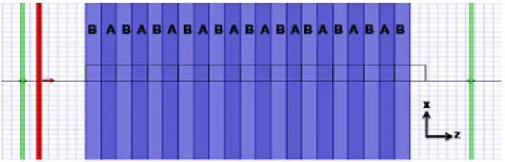
ate the two [1]. In other words due to a long-range order a quasiperiodic system can form forbidden frequency re-gions called pseudo band gaps similar to the band gaps of a PC and simultaneously possess localized states as in disor-dered media [5]. The Fibonacci multilayer structure (well-known quasiperiodic structure) has been studied in past decade, and recently the resonant states at the band edge of the photonic structure in the Fibonacci sequence are stud-ied experimentally, too [6]. A 1D quasi-periodic Fibonacci sequence is based on a recursive relation, which has the form, Sj+1={Sj-1, Sj} for jⰇ1, with S0={B}, S1={A}, S2={BA}, S3={ABA}, S4={BAABA} and so on, where Sj is a structure obtained after j iterations of the generation rule. Here A and B are defined as being two dielectric ma-terials, with different refractive indices (nA, nB) and have geometrical layer thickness (dA, dB). In place of materials A and B, we used air (A) and anisotropic antimony sul-foiodide and antimony selenium iodide (B;SbSI, SbSeI) re-spectively [7]. In Fig. 1 and 2 we show schematically the geometry of conventional PCs and Fibonacci PCs. 1D pho-tonic crystals are characterized by the refractive index con-trast and filling fraction. The refractive index concon-trast is the ratio of the higher refractive index to the lower refrac-tive index in the multiplexer system. The filling fraction f is the ratio between the thickness of the lower refractive index layer(air) and the period of the PC, i.e., f=d1/(d1+d2). A typical 1D PCs and Fibonacci PCs are shown in Fig. 1 and Fig. 2.
Figure 1 1-dimensional SbSI based photonic crystal structure (PCs).
Figure 2 1-dimensional SbSI based Fibonacci photonic crystal structure (FPCs).
The refractive index contrasts of SbSI are taken as follows: na=2.87 nb=3.63 nc=4.55 Tc=22 ºC (paraelectric phase)
2.2 Finite difference time domain (FDTD)
method and plane wave expansion method (PWE)
In our calculations, we used OptiFDTD software package [8]. The OptiFDTD software package is based on the fi-nite-difference time-domain (FDTD) method for transmis-sion spectra and the plane wave expantransmis-sion method (PWE) for photonic band structure.
The photonic band structures of the proposed PCs were calculated by solving the Maxwell equations. The Maxwell equation in a transparent, time-invariant, source free, and non-magnetic medium can be written in the following form:
( )
( )
( )
2 2 1 ω ε c — ¥ — ¥H r = H r r (1)where e r
( )
is the space dependent dielectric function, andc is the speed of light in vacuum. H r
( )
is the magnetic field vector of frequency ω and time dependence ej tw . This equation is sometimes called the Master Equation, and represents an Hermitian eigenproblem, which would not be applicable if the wave equation were derived in terms of the electric field. The Bloch theorem states that, due to infinite periodicity, the magnetic field will take the form( )
jkr( )
k e h = H r r (2) where( )
(
)
k =hk + h r r R (3)for all combinations of lattice vectors R. Thus, Maxwell equation is given in operator form:
(
)
( ) (
)
k 22 k 1 ω j jk ε c È ˘ — ¥ ¥Í — ¥ ˙¥ = Î ˚ k h h r (4)By solving these equations for the irreducible Brillouin zone, we can obtain the photonic band structure.
FDTD algorithm is one of the most appropriate calcula-tion tools [9]. For solving Maxwell's equacalcula-tions depending on the time, FDTD algorithm divides the space and time in a regular grid. Perfect matched layers (PMLs) can be used in the determination of the boundary conditions [10]. In general, the thickness of PML layer in overall simulation area is equal to a lattice constant. FDTD solves electric and magnetic fields by rating depending on space and time and deploys that rating in different spatial regions by sliding each field component half of a pixel. This procedure is known as Yee grid discretization. Fields in these grids can
3 Result and discussion We calculate the spectral
properties in the n-th order (n=10) Fibonacci-type quasipe-riodic layered structures consisting of a A5B6C7 com-pounds. The photonic band structures of 1D A5B6C7 based PCs have been calculated in high-symmetry directions in the first Brillouin. The band structures with transmittance spectra for both photonic crystals are shown in Fig. 4 and Fig. 5. The calculated photonic band structures for both crystals are similar. The all pseudogaps exist in the fre-quencies where the effective refractive index of the struc-ture is positive and the spectral width of the gaps is invari-ant with the change in the transmittance (see Tables 1 and 2). Figures 8 and 9 show the transmittivity of the structure containing a finite number (n=10) layers A and B arranged in the Fibonacci sequence. The positions of the minima in
the transmission spectrum correlate with the gaps obtained in the calculation. A transmission spectrum of a 1D SbSI based PC is compared in Fig. 8 and Fig. 9 with a 1D SbSI based Fibonacci PC. One full period in spectrum which corresponds to the frequency range (0.2-0.5) (ωa/2πc) is presented. Although there is still a gap in the transmission spectrum of the Fibonacci structure around (0.2-0.5) (ωa/2πc), the spectrum is modified significantly. For the SbSeI based PC and Fibonacci PC the results we obtained are very close to the SbSI.
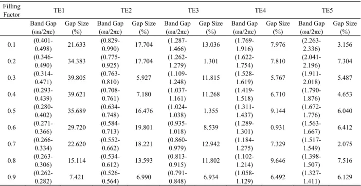
Table 1 Variation of full band gap size for TE modes with filling factor for anisotropic SbSI based layers in air background. Filling
Factor TE1 TE2 TE3 TE4 TE5
Band Gap (ωa/2πc) Gap Size (%) Band Gap (ωa/2πc) Gap Size (%) Band Gap (ωa/2πc) Gap Size (%) Band Gap (ωa/2πc) Gap Size (%) Band Gap (ωa/2πc) Gap Size (%) 0.1 (0.401-0.498) 21.633 (0.829-0.990) 17.704 (1.287-1.466) 13.036 (1.769-1.916) 7.976 (2.263-2.336) 3.156 0.2 (0.346-0.490) 34.383 (0.775-0.925) 17.704 (1.262-1.279) 1.301 (1.622-1.754) 7.810 (2.041-2.196) 7.304 0.3 (0.314-0.471) 39.805 (0.763-0.810) 5.927 (1.109-1.248) 11.815 (1.528-1.619) 5.767 (1.911-2.018) 5.487 0.4 (0.293-0.439) 39.621 (0.708-0.761) 7.180 (1.037-1.161) 11.268 (1.419-1.518) 6.710 (1.790-1.876) 4.653 0.5 (0.280-0.402) 35.689 (0.634-0.748) 16.476 (1.024-1.038) 1.355 (1.311-1.437) 9.144 (1.672-1.776) 6.040 0.6 (0.271-0.366) 29.720 (0.584-0.713) 19.801 (0.935-1.018) 8.539 (1.289-1.301) 0.931 (1.563-1.667) 6.412 0.7 (0.266-0.334) 22.620 (0.552-0.662) 18.221 (0.860-0.979) 12.942 (1.184-1.275) 7.329 (1.517-1.549) 2.075 0.8 (0.263-0.306) 15.114 (0.534-0.612) 13.593 (0.813-0.915) 11.802 (1.102-1.214) 9.646 (1.398-1.507) 7.516 0.9 (0.262-0.282) 7.421 (0.526-0.564) 6.990 (0.791-0.848) 6.934 (1.058-1.129) 6.492 (1.327-1.411) 6.129
The numerical results of variation of full band gap with changing filling factor from 0.1 to 0.9 is given in Tables 1 and 2. Variation of band gap sizes is expressed as a percentage as a function of filling factor and is shown for TE mode in Fig. 5 and Fig. 6. In Fig. 5 and Fig. 6, it is clear that the size of the gap increases with filling fac-tor for the first band gap. The largest gap size is about 38 % when the filling factor is as high as 0.4, but it
de-creases when the filling factor continues to increase. On the other hand, the fifth band gap size does not change too much according to filling factor, but it reaches the minimum value when filling factor is 0.7.
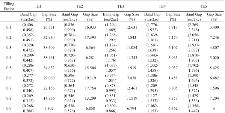
Filling
Factor TE1 TE2 TE3 TE4 TE5
Band Gap (ωa/2πc) Gap Size (%) Band Gap (ωa/2πc) Gap Size (%) Band Gap (ωa/2πc) Gap Size (%) Band Gap (ωa/2πc) Gap Size (%) Band Gap (ωa/2πc) Gap Size (%) 0.1 (0.406-0.498) 20.531 (0.836-0.990) 16.933 (1.294-1.469) 12.631 (1.776-1.922) 7.917 (2.269-2.348) 3.400 0.2 (0.352-0.491) 32.930 (0.781-0.930) 17.393 (1.268-1.292) 1.843 (1.639-1.761) 7.170 (2.056-2.211) 7.246 0.3 (0.320-0.472) 38.409 (0.770-0.820) 6.364 (1.124-1.256) 11.084 (1.541-1.638) 6.102 (1.937-2.032) 4.807 0.4 (0.299-0.442) 38.461 (0.720-0.767) 6.281 (1.051-1.176) 11.243 (1.443-1.532) 5.963 (1.810-1.903) 5.020 0.5 (0.286-0.407) 34.632 (0.650-0.756) 15.504 (1.037-1.057) 1.919 (1.332-1.458) 9.032 (1.702-1.796) 5.425 0.6 (0.277-0.372) 29.060 (0.596-0.722) 19.119 (0.954-1.031) 7.838 (1.306-1.326) 1.458 (1.590-1.696) 6.482 0.7 (0.272-0.340) 22.156 (0.564-0.674) 17.754 (0.878-0.995) 12.461 (1.209-1.295) 6.805 (1.548-1.572) 1.596 0.8 (0.269-0.312) 14.836 (0.546-0.624) 13.299 (0.831-0.933) 11.519 (1.127-1.237) 9.357 (1.429-1.536) 7.204 0.9 (0.268-0.288) 7.302 (0.538-0.576) 6.858 (0.809-0.866) 6.794 (1.082-1.153) 6.362 (1.358-1.442) 6
Figure 3 TE band structure and transmittance spectra of ani-sotropic SbSI.
Figure 4 TE band structure and transmittance spectra of ani-sotropic SbSeI.
field (E) at the left interface of the dielectric layer is simply related to E at the right interface of the same layer by using matrix relation [11]. For 1D structures, it is also possible to compute the electric field distribution inside the sample (Fig. 7). The figure shows the normal-ized field intensity distribution for the wavelength of 1.55 μm on the n-th (n=7) interface.
Figure 7 TE electric field distribution in A5B6C7 based PCs.
Figure 8 TE transmittance spectra of 1D SbSI based PCs.
Figure 9 TE transmittance spectra of 1D SbSI based Fibo-nacci PCs.
4 Conclusion The photonic band structures and
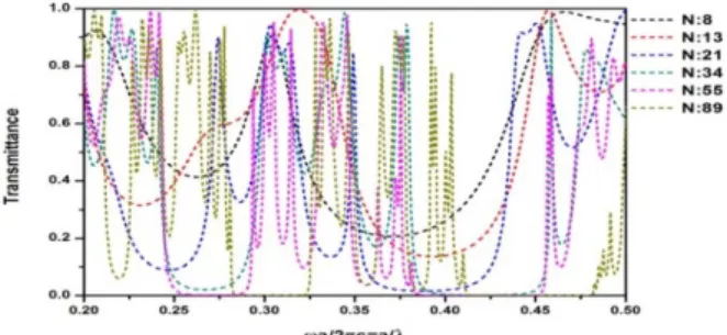
transmission properties of the 1D A5B6C7 PCs consist-ing of dielectric layers immersed in air were studied. We have investigated transmittance spectra of A5B6C7 based both normal PCs and Fibonacci PCs from 8 to 89 layers. The results show that the numbers of pseudo band gaps increase for Fibonacci PCs, when the num-bers of the layers increase.
Acknowledgements This work is supported by the projects DPT-HAMIT, DPT-FOTON, NATO-SET-193 and TUBITAK under Project Nos. 113E331, 109A015, 109E301. One of the authors (Ekmel Ozbay) also acknowledges partial support from the Turkish Academy of Sciences.
References
[1] S. V. Gaponenko, Introduction to Nanophotonics (Cam-bridge University Press, N.Y. 2010), p. 485.
[2] M. Maksimovic and Z. Jaksic, J. Opt. A 8, 355-362 (2006).
[3] A. N. Poddubny and E. L. Ivchenko, Physica E 42, 1871 – 1895 (2010).
[4] A. Rostami and S. Matloub, Opt. Comm. 247, 247-256 (2005).
[5] H. Rahimi, A. Namdar, S. R. Entezar, and H. Tajalli, Prog. Electromagn. Res. 102, 15-30 (2010).
[6] L. Dal Negro, S. J. Oton, Z. Gaburro, L. Pavesi, P. John-son, A. Lagendijk, R. Righini, M. Colossi, and D. S. Wiersma, Phys. Rev. Lett. 90, 055501 (2003).
[7] D. Lusk, I. Abdulhalim, and F. Placido, Opt. Commun. 198, 273-279 (2001).
[8] OptiFDTD 10, http://www.optiwave.com/.
[9] A. Taflove and S. C. Hagness, Computational Electro-dynamics: The Finite-Difference Time-Domain Method, 2nd ed. (Artech House Publishers, Boston, 2000). [10] J. P. Berenger, J. Comput. Phys. 114, 185-200 (1994). [11] F. L. Pedrotti and L. S. Pedrotti, Introduction to Optics