Effect of processing options on ultra-low-loss
lead
–magnesium–niobium titanate thin films for high density capacitors
Wenbin Chen
a,⁎
, Kevin G. McCarthy
b, Shane O'Brien
c, Mehmet Çopuro
ğlu
d, Miao Cai
a,
Richard Win
field
c, Alan Mathewson
ca
Guangxi Key Laboratory of Manufacturing System & Advanced Manufacturing Technology, School of Mechanical and Electrical Engineering, Guilin University of Electronic Technology, 1 Jinji Road, Guilin 541004, Guangxi, China
b
Department of Electrical and Electronic Engineering, University College Cork, Ireland c
Tyndall National Institute, University College Cork, Ireland
dDepartment of Chemistry, Bilkent University, 06800 Bilkent, Ankara, Turkey
a b s t r a c t
a r t i c l e i n f o
Available online 7 January 2013 Keywords:
Loss tangent PMNT Thinfilms Sol–gel
This work studies the impact of annealing temperatures on PMNT (lead–magnesium niobate–lead titanate, Pb(Mg0.33Nb0.67)0.65Ti0.35O3) thinfilms grown on a silicon substrate. The electrical properties of the thin
films, such as dielectric constant and loss tangent, are shown to depend strongly on the annealing tempera-ture, with the best electrical properties being achieved at the highest annealing temperature. It is seen that the perovskite phase is highest in the sample annealed at 750 °C indicating that a relatively high temperature is necessary for complete transition of PMNT to the perovskite phase. The sample annealed at 400 °C exhibits the lowest loss tangent of approximately 0.007 at a frequency of 1 MHz.
© 2013 Elsevier B.V. All rights reserved.
1. Introduction
PMNT (lead–magnesium niobate–lead titanate, Pb(Mg0.33Nb0.67) 0.65Ti0.35O3) ferroelectric material has been shown to have promising
characteristics for the formation of high-performance, low cost, thin films for integrated circuit (IC) applications. These thin films have high dielectric constants and low leakage currents and are therefore suitable for use as the insulator layers of high-density capacitors (with a high capacitance per unit area) in integrated circuits for small, low-power, portable, silicon electronic systems[1–3]. How-ever, like any material system that is proposed for incorporation into an integrated circuit fabrication process, PMNT must be extensively characterised, and the trade-offs between processing conditions and the electrical performance understood, before the material can be considered for integration. This paper studies one of the important trade-offs, the annealing temperature, and outlines how the electrical properties of the PMNT thinfilms vary for a range of annealing temper-atures from 400 °C to 750 °C.
2. Sample fabrication
The PMNT thinfilms were grown on a Pt(111)/TiO2/SiO2/Si substrate
using a sol–gel technique[4–6]. All the chemicals employed were sup-plied by Sigma-Aldrich Co. Mg(C2H5O)2, Nb(C2H5O)5, Ti(n-C3H7O)4,
2-methoxyethanol (2ME), formamide and 1-hydroxy-cyclohexyl phe-nyl ketone (1HPK) were used as received. Pb(C2H3O2)2·3H2O was
dehydrated in a laboratory vacuum oven (Heraeus VT 5042 EK) at 70 °C for 16 h prior to use. A 0.5 M Pb(Mg0.33Nb0.67)0.65Ti0.35O3+ 15%
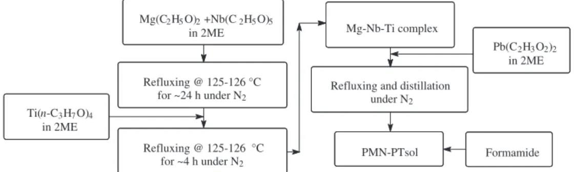
PbO was synthesised by the sol–gel method, a flowchart of which is given inFig. 1, resulting in a clear yellow/light brown sol. A stabiliser (formamide) amounting to 4% by volume was added. The precise concentration was adjusted by adding extra 2ME, where necessary. The sol–gel was spin-coated using a WS-400A-6NPP/LITE Spin-Coater (Laurell Technologies) at a spin rate of 3000 rpm for 30 s at room-temperature (RT). The coated wafers were then transferred onto a hot-plate, which had been set to 300 °C and kept at this temperature for approximately 1 min. The wafers were then allowed to rest at RT for approximately 30 s. The samples were then annealed using a Jipelec Jetfirst 150 rapid thermal processor at the desired annealing tempera-ture in an O2atmosphere[5]. The spin-coating and annealing cycles
were repeated three times to obtain the desired film thicknesses. Samples were prepared with four annealing temperatures — these temperatures and the associated film thicknesses are as follows: 400 °C (128.2 nm), 450 °C (475 nm, estimated), 600 °C (147.6 nm) and 750 °C (380 nm).
Following growth and annealing of the PMNT layers, a composite top metal layer was deposited and patterned to form capacitor test structures which allow the dielectric properties of the PMNT to be measured. The composite top metal layer consists of 100 nm Pt and 200 nm Au. The Pt has good adhesion properties to the PMNT and the Au is used to reduce the overall resistance of the top metal layer and give good electrical contact to the probes used for measurement. Thin Solid Films 541 (2013) 117–120
⁎ Corresponding author. Tel.: +86 15907886352. E-mail address:[email protected](W. Chen).
0040-6090/$– see front matter © 2013 Elsevier B.V. All rights reserved.
http://dx.doi.org/10.1016/j.tsf.2012.12.092
Contents lists available atSciVerse ScienceDirect
Thin Solid Films
This top Pt/Au layer was patterned by photography and a lift-off pro-cess to create thefinal capacitor test structures. A cross-section and a top view of the test structures are shown inFig. 2. Capacitors from the top metal layer to the underlying Pt layer are formed by simple square pad structures of dimensions 125μm×125 μm as shown.
The crystal structure of the samples was determined by X-ray diffraction (XRD) using a PANalytical “X'Pert PRO XRD” system, using copper Kα1radiation. XRD patterns were recorded in the normal
Θ/2Θ mode.
Scanning electron microscope (SEM) images were obtained using an FEI NovaNano 630, high-resolution, SEM instrument. The SEM accelerator voltage was adjusted to ensure good contrast, while mitigating the effects of charging, with a value of 20 kV for the 400 °C and 600 °C samples and 6 kV for the 750 °C sample.
The capacitance and loss tangent of the test capacitors were measured at zero-bias at frequencies up to 2 MHz using an HP4284A precision LCR meter[3]. The capacitors were contacted by means of metal probes in an electrically and light-shielded probe station which were connected to the LCR meter by means of low-leakage, shielded cables. To zero any offsets in the system, the capacitance wasfirst measured with the probes raised in the air above the samples and this offset was subtracted from the capacitance measured with the probes touching the samples. The dielectric constant was determined by rearrangement of the standard capacitance formula
C¼εOεr tD ⋅A⇒εr¼ C A ⋅ tD εO ð1Þ
whereεois the permittivity of free-space,εris the relative permittivity
(dielectric constant) of the dielectric thinfilm, tDis the thickness of the
thinfilm and A is the area of the capacitor. 3. Physical properties
Fig. 3shows the XRD data for PMNT samples annealed at 400 °C, 600 °C and 750 °C, respectively. The dominant peak in each of the plots corresponds to the perovskite phase of the material with the lower peaks corresponding to the pyrochlore phase and to the Si substrate. It is seen that the perovskite phase is highest in the sample annealed at 750 °C indicating that a relatively high temperature is necessary for complete transition of PMNT to the perovskite phase.
Fig. 4shows the SEM images of the samples annealed at 400 °C, 600 °C and 750 °C, respectively. In these SEM images all thefilms appear dense and compact and there is no evidence of porosity (pinholes) in thefilms [6]. This is further evidenced by the very small leakage current in the films as indicated by the low loss tangents observed in the electrical measurements.
When the samples annealed at 400 °C and 600 °C were inspected in an optical microscope some areas of the samples displayed a green colour unlike the other samples. Such colour changes can indicate minor thickness inhomogeneity which can occur as part of the spinning process when excess liquid is pushed from the centre of the samples to the sides resulting in thefilms being thicker at the edges than in the centre. Electrical measurements were performed for both the normal and the coloured areas of these samples. 4. Electrical properties
Fig. 5 presents the electrical measurements for the samples annealed at different temperatures. In all cases, the thinfilms display a high dielectric constant accompanied by a low loss tangent. A general trend across all the samples is that the dielectric constant decreases with frequency across most of the frequency range and the loss tangent follows a similar trend. For calibration purposes, other test capacitors were fabricated with SiO2 as the dielectric
layer and these samples displayed dielectric constant and loss tangent across the frequency range, indicating that the measurement setup was performing an accurate measurement over frequency and the behaviour indicated for the PMNT samples inFig. 5 represents the intrinsic behaviour of the material and is not an artefact of the measurement setup.
Fig. 5illustrates the strong relationship between the annealing temperature and the dielectric properties of the PMNT thinfilms. At a frequency of 1 MHz, the samples annealed at 400 °C have a dielectric constant of approximately 14, those annealed at 450 °C have a dielectric constant of approximately 80 while the samples annealed at 750 °C achieve an exceptionally high dielectric constant of approximately 1115. As indicated by the XRD data presented in Fig. 3, higher annealing temperatures favour the formation of the perovskite phase of the material compared to the pyrochlore phase Mg(C2H5O)2+Nb(C2H5O)5 in 2ME Ti(n-C3H7O)4 in 2ME Pb(C2H3O2)2 in 2ME Refluxing @ 125-126 °C for ~24 h under N2 Refluxing @ 125-126 °C for ~4 h under N2 PMN-PTsol Mg-Nb-Ti complex Formamide Refluxing and distillation
under N2
Fig. 1. Flowchart of the sol–gel synthesis process.
m
m
m
m
m
m
m
m
µ
m
µ
2µ
m
m
µ
D 2Fig. 2. Cross-section and top view of the fabricated capacitor test structures.
Fig. 3. XRD patterns of PMNT samples of different thickness prepared with no nucleation seed after annealing at 400, 600 and 750 °C (For peak assignment, S=substrate, 1=pyrochlore, 2=perovskite).
Fig. 4. Tilted SEM image (45°) of PMNT samples of different thickness prepared with no nucleation seeds after annealing at 400, 600 and 750 °C. Image of the sample annealed at 750 °C is reproduced from[3].
Fig. 5.εrand loss tangent of PMNT samples annealed at 400, 450, 600 and 750 °C. Measurements have been taken on the centre areas and on the edge regions of the samples for the ones annealed at 400 and 600 °C.
119 W. Chen et al. / Thin Solid Films 541 (2013) 117–120
at lower temperatures and the dielectric constant is thus seen to increase as the perovskite phase becomes dominant. The measure-ments shown in Fig. 5 indicate that the dielectric constant has improved by a factor of almost 100 when the annealing temperature changes from 400 °C to 750 °C, indicating the dramatic difference be-tween the pyrochlore and perovskite phases of the material. The loss tangent is low for all the samples shown. At a frequency of 1 MHz it is lowest at approximately 0.007 for the sample annealed at 400 °C and rises to approximately 0.02 for the sample annealed at 750 °C. While this indicates some degradation in the loss tangent for the sample annealed at 750 °C, this would be an acceptable trade-off with the very high dielectric constant of approximately 1115 in many applica-tions. The sample annealed at 600 °C follows the general trend in the loss tangent but deviates from the trend for the dielectric constant having the lowest dielectric constant of all the samples. For the samples with the colour variations, the measurements for the normal and coloured areas follow the same general trends with frequency but show slightly different values consistent with small variations in the thickness of the PMNT thinfilm layers.
5. Conclusions
The electrical characteristics of capacitor test structures based on the PMNT thinfilm layers have been presented. The electrical proper-ties have been shown to be strongly influenced by the annealing temperature, with the dielectric constant changing by a factor of almost 100 as the annealing temperature is changed from 400 °C to 750 °C, corresponding to the material changing from the pyrochlore phase to the perovskite phase. The results show that the perovskite
phase is highest in the sample annealed at 750 °C indicating that a relatively high temperature is necessary for complete transition of PMNT to the perovskite phase. The sample annealed at 400 °C exhibits the lowest loss tangent of approximately 0.007 at a frequency of 1 MHz. PMNT is therefore a promising material for high density capacitor applications in future integrated circuit processes if the annealing temperature required to form the perovskite phase can be lowered.
Acknowledgements
This work was supported in part by the European Union Sixth Framework Programme through STREP project 033103 (CAMELIA). W. Chen also received support from PRTLI 4— NEMBES. Some of the measurements reported here were facilitated by Science Foundation Ireland National Access Programme, project NAP351. This research was also supported by Guangxi Key Laboratory of Manufacturing System & Advanced Manufacturing Technology (Grant No. 11-031-12_001) and Guangxi Natural Science Foundation (2012GXNSFFA060010).
References
[1] E. Fribourg-Blanc, E. Cattan, D. Remiens, E. Defay, Solid State Electron. 47 (2003) 1631.
[2] X. Zhu, E. Defay, A. Suhm, E. Fribourg-blanc, M. Aid, Appl. Phys. Lett. 94 (12) (2009). [3] W. Chen, K.G. McCarthy, A. Mathewson, M. Copuroglu, S. O'Brien, R. Winfield, IEEE
Electron Device Lett. 3 (1/9) (2010) 996.
[4] D. Kuscer, J. Holc, M. Kosec, J. Am. Ceram. Soc. 90 (1) (2007) 29.
[5] W. Chen, K. McCarthy, M. Copuroglu, S. O'Brien, R. Winfield, A. Mathewson, Thin Solid Films 520 (2012) 4523.
[6] W. Chen, K. McCarthy, M. Copuroglu, H. Doyle, B. Malic, B. Kuznik, M. Kosec, S. O'Brien, R. Winfield, A. Mathewson, Thin Solid Films 519 (2011) 5800.