Air-Stable
n‑channel Diketopyrrolopyrrole−Diketopyrrolopyrrole
Oligomers for High Performance Ambipolar Organic Transistors
Tushita Mukhopadhyay,
†Boregowda Puttaraju,
†Satyaprasad P. Senanayak,
‡Aditya Sadhanala,
‡Richard Friend,
‡Hendrik A. Faber,
§Thomas D. Anthopoulos,
§Ulrike Salzner,
∥Andreas Meyer,
⊥and Satish Patil
*
,††Solid State and Structural Chemistry Unit, Indian Institute of Science, Bangalore 560012, India
‡Cavendish Laboratory, Department of Physics, University of Cambridge, Cambridge CB3 0HE, United Kingdom
§Department of Physics and Centre for Plastic Electronics, Blackett Laboratory, Imperial College London, London 7W72BW, United Kingdom
∥Department of Chemistry, Bilkent University, 06800 Bilkent/Ankara, Turkey ⊥Institut für Physikalische Chemie, Universität Hamburg, 20148 Hamburg, Germany
*
S Supporting InformationABSTRACT: n-channel organic semiconductors are prone to oxidation upon exposed to ambient conditions. Herein, we report design and synthesis of diketopyrrolopyrrole (DPP)-based oligomers for ambipolar organic thin-film transistors (OFETs) with excellent air and bias stability at ambient conditions. The cyclic voltammetry measurements reveal excep-tional electrochemical stability during the redox cycle of oligomers. Structural properties including aggregation, crystallinity, and morphology in thin film were investigated by UV−visible spectroscopy, atomic force microscopy (AFM), thin-film X-ray diffraction (XRD), and grazing incidence small-angle X-ray scattering (GISAXS) measurements. AFM reveals morphological changes induced by different processing conditions whereas GISAXS measurements show an increase in the population of face-on oriented crystallites infilms subjected to a combination of solvent and thermal treatments. These measurements also highlight the significance of
chalcogen atom from sulfur to selenium on the photophysical, optical, electronic, and solid-state properties of DPP−DPP oligomers. Charge carrier mobilities of the oligomers were investigated by fabricating top-gate bottom-contact (TG−BC) thin-film transistors by annealing the thin thin-films under various conditions. Combined solvent and thermal annealing of DPP−DPP oligomer thinfilms results in consistent electron mobilities as high as ∼0.2 cm2V−1s−1with an on/off ratio exceeding 104.
Field-effect behavior was retained for up to ∼4 weeks, which illustrates remarkable air and bias stability. This work paves the way toward the development of n-channel DPP−DPP-based oligomers exhibiting retention of field-effect behavior with superior stability at ambient conditions.
KEYWORDS: TFT, oligomers, aggregation, crystallinity, annealing, n-channel
1. INTRODUCTION
Organic thin-film transistors (OFETs) have potential applica-tions in numerous electronic devices such as displays, integrated circuits (IC), and radio frequency identification (RFID) tags.1Recently, the performance of p-channel OFETs has increased notably, as polymeric semiconductors with hole mobilities of 6−23 cm2 V−1 s−1 have been reported.2
Unfortunately, n-channel OFETs fabricated using organic semiconductors are notoriously prone to oxidation within minutes of air exposure.3 The low performance of n-channel OFETs is recognized as a serious limitation for fabrication of rectifying junctions.4 However, ambipolar transistors are the fundamental building blocks of modern electronic devices such as bipolar transistors’ complementary logic circuits, inverters,
and printed ring oscillators.5Hence, it is essential to develop π-conjugated semiconductors with ambipolar transport.6,7 To fully realize n-channel OFETs, organic semiconductors should meet the following criteria: (i) anions formed by electron injection should be stable upon exposure to ambient conditions, especially toward water and air; (ii) the electron affinity should match the Fermi levels of an environmentally stable electrode (Au or Ag) for optimal electron injection; (iii) the intermolecular overlap of semiconductor LUMOs should be large with minimum traps to facilitate electron hopping.3 In
Received: July 18, 2016 Accepted: September 5, 2016 Published: September 5, 2016
Research Article
www.acsami.org copying and redistribution of the article or any adaptations for non-commercial purposes.
Downloaded via BILKENT UNIV on December 23, 2018 at 17:55:09 (UTC).
addition, many other factors such as thin-film morphology, molecular packing, and interface between dielectric and semiconductor need to be optimized to achieve high perform-ance ambipolar organic transistors.8 By now, chemistry design approaches have been developed to effectively meet these criteria.9 Ambipolar transport has been realized in donor− acceptor-based conjugated polymers.10,11In donor−acceptor π-conjugated systems, backbone co-planarity and good intra-molecularπ-orbital overlap leads to delocalized occupied and unoccupied frontier molecular orbitals which are essential for ambipolar charge transport. Remarkable progress in the performance of optoelectronic devices has been realized by incorporating DPP units in polymers and oligomers.12−14DPP is comprised of an electron deficient fused lactam ring, flanked by donors. With the DPP acceptor unit, the frontier molecular orbital positions and the intramolecular and intermolecular interactions can be tuned to achieve the desired optoelectronic and transport properties.15,16
Several research groups have carried out backbone and side-chain architectural modifications on DPP-based conjugated materials by increasing the electron deficiency of the backbone thereby stabilizing the n-channel OFET against ambient oxidation. Qiao et al. have increased the DPP backbone planarity and electron affinity by covalently linking DPP with dicyanomethane to obtain electron mobilities of 0.55 cm2V−1 s−1.17Semiconductor−dielectric interface modifications by self-assembly techniques and usage of low work function top electrodes can effectively extract electrons.8,18 Side-chain engineering has been shown to be pivotal in altering molecular packing and backbone torsional conformations.12For example, Lee et al. obtained an electron mobility of 4.34 cm2V−1s−1in a
DPP−selenophene copolymer by varying the alkyl spacer length in a hybrid siloxane group.19 Kanimozhi et al.
demonstrated the role of triethylene glycol side chains in a DPP−DPP-based copolymer to obtain electron mobilities as high as ∼3 cm2 V−1 s−1.20,21 The modification of backbone dipole orientations and the promotion of halogen−chalcogen supramolecular interactions by heavy atom introduction have been shown to improve electron and hole mobilities.22,23Sun et al. reported the highest electron mobility of 6.3 cm2V−1s−1by combining pyridine with DPP which leads to highly crystalline
polymers and oriented thin films.24 Coupling DPP to
selenophene has resulted in higher hole and electron mobilities (1.62 and 0.14 cm2 V−1 s−1) compared to their thiophene counterparts.25−27DPP−vinylene and selenophene−vinylene− selenophene-based co-polymers have shown electron mobilities of∼0.05 cm2V−1s−123and hole mobilities as high as 4.97 cm2 V−1 s−1.26 Various film processing techniques have been implemented to promote self-assembly in thinfilms to enhance n-channel charge carrier mobilities. Off-center spinning is one such technique which makes use of directional forces to align the chains radially with respect to the transistor channel.28 Thermal and solvent annealing techniques29 and controlled solvent evaporation rate using a mixture of high boiling and low boiling solvents,30etc., have also helped to achieve remarkable enhancements in charge carrier mobilities.
The research discussed so far is based on donor−acceptor π-conjugated polymers. Polymers, however, inherently suffer from conformational, structural, and positional disorder which results in torsional defects and chain entanglements.31,32These phenomena reduce the effective conjugation length and increase π−π stacking distances leading to a lower degree of thin-film crystallinity and higher activation energy for charge carrier hopping.33 Tail states within the band gap of such systems and chemical traps originating from end groups localize charge carriers and adversely affect substrate−polymer Scheme 1. Synthetic Scheme for Four DPP-Based Oligomers
interaction energies.34 The strong dependence of charge transport properties on molecular weight and polydispersity impedes the elucidation of the fundamental charge transport mechanisms and structure−property correlations in polymeric systems. It is therefore important to design model compounds with low defect densities and improved solution process-ability.35In this regard, oligomers inherit the long-range order, low defect density of crystals and retain the goodfilm-forming abilities of polymers. Oligomers have well-defined and monodisperse molecular structures and show minimum batch-to-batch variation during synthesis.36Herein, we report synthesis, photophysical, and transport properties of four air-stable n-channel DPP-based oligomers. We systematically varied the central unit for linking DPP to DPP and probed the role of aggregation and torsional defects on photophysical properties using UV−visible spectroscopy. We found that although torsional defects influence self-organization and the degree of order in thinfilms, they have negligible influence on transport properties of DPP−DPP oligomers. Notably, room temperature solvent annealing and thermal treatment further enhance crystallinity and reduce dispersion in the population of microstructures possessing long-range order. We refer to these samples as as-cast (AC), solvent annealed (SA), thermally annealed (TA), and solvent and thermally annealed (STA) throughout this work. The unique structural organizational
features such as π−π stacking originated after different annealing processes were probed by grazing incidence small-angle X-ray scattering (GISAXS) and X-ray diffraction (XRD) measurements. Subsequently, transport properties TG-BC in field-effect transistor geometry has been measured for AC, SA, TA, and STA samples. The STA samples gave rise to superior electron mobility of up to 0.16 cm2V−1s−1with enhanced air
stability.
2. RESULTS AND DISCUSSION
2.1. Synthesis and Characterization. The four oligomers shown in Scheme 1are end-capped with a phenyl group and
have been named as TDPP−BTZ−TDPP, TDPP−TDPP−
TDPP, TDP−SeDPP−TDPP, and TDPP−PDPP−TDPP. The
oligomers were synthesized by a Suzuki cross-coupling reaction involving appropriate monomers having a boronic ester functionality in the presence of a palladium catalyst Pd2(dba)3with an active ligand P(o-tol)3. The crude oligomers
were precipitated in methanol and further purified through Soxhlet extraction in hot methanol and acetone to remove unreacted starting materials and byproducts. The terminal monomers have been functionalized with long and branched 2-octyldodecyl side chains to increase theirfilm-forming abilities. The central monomers have been N-alkylated with the short
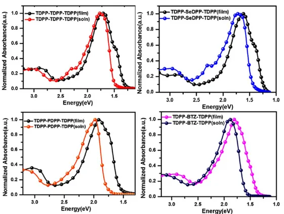
Figure 1.Comparison of solution and as-cast (AC) thin-film UV−visible spectra of four DPP-based oligomers.
Table 1. Summary of UV−Vis and Electrochemical Properties of Four DPP-Based Oligomers UV−vis absorption spectra
λmax(eV) electrochemical properties
oligomer solution film Egopt(eV) Eox(eV) Ered(eV) Egelec(eV)
TDPP−TDPP−TDPP 1.77 1.67 1.30 5.29 3.62 1.70
TDPP−SeDPP−TDPP 1.73 1.60 1.20 5.17 3.65 1.50
TDPP−PDPP−TDPP 1.99 1.91 1.70 5.32 3.52 1.80
TDPP−BTZ−TDPP 1.89 1.80 1.50 5.28 3.53 1.75
hexyl chain to facilitate greater solid-state packing. Structural characterization of the monomers and the oligomers was carried out using1H NMR and 13C NMR spectroscopies and mass spectrometry (Supporting Information (SI) Figures S1− S21).
2.2. Optical Properties and Electronic Structure. The optical properties of the oligomers, in particular the effect of the donor on backbone planarity and aggregation during different film processing methods, have been investigated by UV−visible spectroscopy. The UV−visible spectra in solution and AC thin films are shown inFigure 1, and the peak positions are listed in Table 1. Thin films of all four oligomers exhibit dual band absorption spectra typical of donor−acceptor-based sys-tems.23,37 Solution spectra of TDPP−TDPP−TDPP and
TDPP−SeDPP−TDPP exhibit a third band between the
other two. All absorption bands show a gradual bathochromic shift on going from TDPP−PDPP−TDPP to TDPP−BTZ−
TDPP to TDPP−TDPP−TDPP and TDPP−SeDPP−TDPP.
The reduction in the optical gap may be due to reduced aromaticity of the donor which varies as phenyl\>thiophene \>selenophene. The lower aromaticity of selenophene shortens the interring donor−acceptor bond and decreases the band gap by destabilizing both HOMO and LUMO.38Selenium is larger and therefore more polarizable than thiophene and has lower ionization energy. This makes selenophene a slightly stronger electron donor than thiophene.39−41 Kanimozhi et al. have shown previously that the larger band gap of phenyl systems is mainly due to the electronic nature of the phenyl ring.31Steric interactions between the alkyl hydrogens and the ortho hydrogens of the phenyl group, which induce a twist angle of ∼35° between the phenyl ring and DPP, lead to a small additional blue shift in the solution phase. Hence, the absorption energy of TDPP−PDPP−TDPP (1.99 eV) is larger
than those of TDPP−TDPP−TDPP (1.77 eV) and the
TDPP−SeDPP−TDPP (1.73 eV). TDPP−BTZ−TDPP
ab-sorbs between the phenyl and chalcogenyl systems at 1.89 eV. A detailed analysis of the spectra is presented in the theoretical part below. The association of the oligomers on solid substrates can be controlled by thermal and solvent−vapor annealing which assists the organization into ordered structures. The aggregation behavior of the oligomers under different thin-film processing conditions is shown in Figure S22, SI. Annealing treatments further induce interactions between extended oligomer chains leading to aggregate formation. The differences in the relative orientation of the dipole moments in AC, TA, SA, and STAfilms manifest themselves as red/blue shifts in the absorption spectra, depending on the annealing conditions. The aggregation-dependent spectral shifts can also be attributed to Davydov splitting.42When the chain dipole moments arrange in a head-to-tail fashion, there is a red shift in the absorption spectra whereas a blue shift implies a parallel arrangement.43,44 In TDPP−TDPP−TDPP oligomers, a significant red shift is seen in TA, SA, and STAfilms. In contrast, spectral shifts in
TA, SA, and STA films of TDPP−SeDPP−TDPP are
insignificant. TDPP−PDPP−TDPP shows an interesting
response to thermal and solvent annealing. The low energy vibronic feature is enhanced on solvent annealing showing an increased aggregation tendency. This implies that there is an increase in population of the molecular transition dipoles which are arranged in a head-to-tail fashion. On thermally annealing the AC and SA films, the spectral broadening is further enhanced implying increased aggregation at higher temper-ature. There is a minor spectral red shift in the
post-thermally-annealedfilms, as compared to the AC and SA films. For the TDPP−BTZ−TDPP oligomer, the TA and the STA films show the evolution of a resolvable vibronic feature while for the solvent treated film there is a slight bathochromic shift along with the evolution of a vibronic feature near the absorption edge. Such differences in the aggregation behavior under varying processing conditions have important implications on charge transport properties as discussed in subsequent sections. 2.3. Electrochemical Properties. The electrochemical properties of the oligomers were investigated by cyclic voltammetry (CV). Platinum electrodes were used as working and counter electrodes, where Ag/Ag+ have been employed as the reference electrode. Energy levels have been calibrated with respect to an internal standard ferrocene/ferrocenium redox couple.
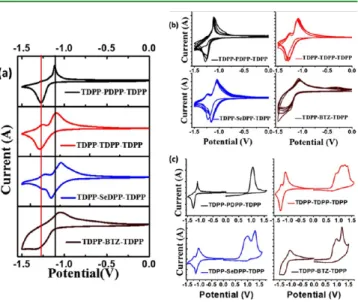
Voltammograms are shown inFigure 2. Electrochemical and optical data are compared inTable 1. As shown inFigure 2a,
the onset of the reduction potential gets more negative from
TDPP−PDPP−TDPP to TDPP−BTZ−TDPP, while the onset
of oxidation is less affected. The CVs of oligomers reveal reversible reductive processes and quasi-reversible oxidation cycles (Figure 2c). The stability of the reductive cycle is verified by CV with multiple cycles in negative potential as shown in Figure 2b. We observed a shift of the peak potential during the first cycles before it stabilizes. The shift is presumably due to low reorganization energy of the oligomer backbones.45 The electrochemical data indicate that the oligomers are extremely stable during electrochemical reduction.
The ionization energies were also obtained from ultraviolet photoemission spectroscopy (UPS) and extracted from the plots as shown in Figures S23−S24, SI. The positions of HOMO and LUMO levels as elucidated from UPS measure-ments corroborate well with the redox potential values obtained from electrochemical values. The intrinsic nature of charge carriers can be estimated by evaluating the difference between frontier orbitals and Fermi levels. The difference between the Fermi energies and LUMO (obtained from electrochemical measurements, Table 1) follows this trend: TDPP−SeDPP− TDPP (0.33 eV) < TDPP−TDPP−TDPP (0.45 eV) < TDPP−
BTZ−TDPP (0.59 eV) < TDPP−PDPP−TDPP (0.71 eV).
Figure 2.Cyclic voltammograms of four DPP-based oligomers: (a) negative cycle, (b) negative cycle for multiple segments, and (c) complete redox cycle at 0.1 V/s scan rate.
The energy difference between HOMO and Fermi energy levels follows this sequence: TDPP−SeDPP−TDPP (0.65 eV)
< TDPP−TDPP−TDPP (0.52 eV) < TDPP−PDPP−TDPP
(0.71 eV) < TDPP−BTZ−TDPP (0.70 eV). The relatively low energy difference between the frontier levels and Fermi level of TDPP−SeDPP−TDPP shows that it stabilizes the LUMO and
Figure 3.Thin-film X-ray diffractograms of DPP-based oligomers.
Figure 4.GISAXS of four DPP-based oligomers under different annealing conditions.
destabilizes the HOMO. Similarly, the trends in the electro-chemical gaps follow those in the optical gaps, although electrochemical gaps are larger by∼0.4, 0.3, 0.1, and 0.3 eV for
TDPP−TDPP−TDPP, TDPP−SeDPP−TDPP, TDPP−
PDPP−TDPP, and TDPP−BTZ−TDPP, respectively. These
differences can be accounted for by the interface barrier between electrode and oligomer film and by the exciton binding energy. The observed trend indicates that the large electron affinities of selenophene and benzothiadiazole reduce the electrochemical band gaps and cause the substantial red shift in the optical band gap.
2.4. Thin-Film X-ray Diffraction Measurements. The samples annealed with different processes (AC, SA, TA, and STA) were investigated by X-ray diffraction as shown inFigure 3. The diffusion of solvent vapors into the films enables formation of a “soft phase” which imparts a high degree of freedom for reorganization of the oligomers in thinfilms.46,47
The d-spacing on solvent annealing implies a favorable interdigitation of the alkyl chains which helps to establish better connectivity of the oligomer units along the lamellae for enhanced charge transport. The films were subjected to chloroform vapor, for a period of 30 min in a sealed Petri dish. Small d-spacing (enhanced crystallinity) is an important factor that facilitates charge transport. Grain sizes can be estimated from the full width at half-maximum (fwhm) values by fitting a Gaussian to the peaks corresponding to lamellar packing. The fwhm values along with the d-spacing have been tabulated in Table S1a,SI. We observed that the d-spacing is less infilms that have been subjected to solvent vapor (SA films than TAfilms). We find that there is a minor increase in the fwhm values in SA films as compared to TA and STA films, implying that there is a decrease in crystallinity. This indicates that solvent annealing leads to enhanced crystallinity in the thin film with a broader distribution of crystallite size. Apart from
Figure 5.Height images obtained by atomic force microscopy (noncontact mode) for four DPP-based oligomers (scale bar, 4μm).
the variations in d-spacings and fwhm, we observed changes in the peak intensities for different annealing conditions, as shown in Figure S29, SI, which reveals that a combination of STA leads to high crystallinity to the thinfilms of all oligomers.
2.5. Grazing Incidence X-ray Diffraction Measure-ments. In a π-conjugated system, nonbonding interchain interactions govern the π−π stacking of the molecular backbones. To reduce the charge carrier hopping barrier, these stacks must have a the proper orientation with minimum tilt between stacked planes, enhanced microstructural order, and reduced grain boundary defects. The lamellar d-spacing must be as small as possible. A more detailed view such as the orientation degree of the stacks, thickness of the lamellae in the domains, and lamellar d-spacing is found by GISAXS measurements. The two-dimensional scattering patterns are shown inFigure 4. The oligomers exhibit face-on orientation irrespective of the film processing method. Interestingly, we observed substantial structural differences between the AC, SA, TA, and STAfilms of oligomers. The AC films of both TDPP−
TDPP−TDPP and TDPP−SeDPP−TDPP show less intense
diffraction spots on the Qxyaxis while those of TDPP−PDPP−
TDPP and TDPP−BTZ−TDPP show intense spots with arc-like features. The presence of arc-arc-like features indicates the existence of both edge-on and face-on oriented crystallites in thefilm and the presence of grain boundaries. The simplified Herman’s orientation function “f ” follows the order for AC film: TDPP−TDPP−TDPP (0.952) > TDPP−SeDPP−TDPP
(0.918) > TDPP−PDPP−TDPP/TDPP−BTZ−TDPP
(0.911). The lamellar d-spacing of TDPP−PDPP−TDPP and
TDPP−BTZ−TDPP are larger than those of TDPP−TDPP−
TDPP and TDPP−SeDPP−TDPP. As a result the films of
TDPP−TDPP−TDPP and TDPP−SeDPP−TDPP exhibit
better adjacent “interchain electronic coupling” and are inherently more ordered with better oriented and larger crystallites than those of TDPP−PDPP−TDPP and TDPP− BTZ−TDPP. The detailed structural results obtained from 2D GISAXS analysis are listed in Table S1b,SI. The domain size
follows the order in AC films: TDPP−SeDPP−TDPP >
TDPP−TDPP−TDPP > TDPP−BTZ−TDPP > TDPP−
PDPP−TDPP. The stronger the interaction between the oligomer backbones, the greater is the extent of solid-state packing and the larger is the domain size. Backbone interaction energy is a cumulative effect of electrostatic, dispersion, and induction forces. Because selenium is soft and more polarizable than sulfur, the induction and dispersion forces are stronger in TDPP−SeDPP−TDPP which drives the association of the chains in the solid state via strong nonbonding interchain forces arising from Se···C−H σ* interactions.48
Although STAfilms have a higher degree of orientation than TA and SAfilms (as indicated by the f values shown in Table S1b, SI), the crystallinity (d-spacing) of STA films is comparable to those of TA and SAfilms. In SA films, the d-spacings are smaller compared to those in TAfilms for TDPP−
TDPP−TDPP and TDPP−SeDPP−TDPP, whereas, for
TDPP−PDPP−TDPP and TDPP−BTZ−TDPP, the
d-spac-ings are unchanged. This shows that crystallinity induced by solvent vapor is comparable to that induced by thermal annealing. SAfilms have a reduced degree of flat-on orientation as compared to TAfilms as manifested in their lower f values. The degree of stacking improves on thermal treatment of the SAfilms which is implied by a higher degree of microstructural order and fewer grain boundary defects in STAfilms. Although the order in the stacks improves in STAfilms of TDPP−BTZ−
TDPP compared to TDPP−PDPP−TDPP, it is to be noted
that TDPP−BTZ−TDPP has smaller domain sizes than
TDPP−PDPP−TDPP. Although TDPP−TDPP−TDPP and
TDPP−SeDPP−TDPP show disorder in the stacks in STA
films compared to TDPP−PDPP−TDPP and TDPP−BTZ− TDPP, their domain sizes (thickness per lamellar stack) are larger. Thermal annealing of SAfilms results in the removal of the grain boundaries created due to nonuniform crystallization in the film thereby increasing the stacking order. In TDPP− PDPP−TDPP oligomer, we observed that the STA film has minimum arc-like features, which means that the crystallites are highly oriented. The (010) peak intensity versus azimuthal angle plots are shown in the Supporting Information (Figure S25).
2.6. Morphological Studies. The changes in the thin-film morphology of these materials by different annealing treat-ments were probed by AFM using the noncontact mode. The thinfilms were prepared by spin coating from dilute solutions of the oligomers from a mixture of chlorobenzene and chloroform, and AFM images are shown in Figure 5. Solvent annealing was carried out by keeping thefilms in a sealed Petri dish under chloroform vapor atmosphere for 30 min. STAfilms were prepared by annealing the SAfilms for 30 min at their melting temperatures as obtained from DSC measurements. We observed that the nucleation phenomenon was critically influenced by different annealing treatments.49 Apart from crystallinity, grain sizes and densities, and their connectivities are also affected by different film processing methods. Post-thermal and solvent treatments induce aggregation. The TA film of TDPP−TDPP−TDPP is comprised of fibers. On solvent annealing, the length of thefibers is shorter. On further thermal annealing, there is little change in the morphology. The STAfilm has a greater roughness of 27 nm compared to the SA film (13 nm). The STA film of TDPP−SeDPP−TDPP has a roughness of 26 nm whereas the SAfilm has a roughness of 16 nm. We observe that the root-mean-square roughness of STA films of TDPP−PDPP−TDPP and TDPP−BTZ−TDPP are 99 and 23 nm, respectively. SAfilms of TDPP−PDPP−TDPP and TDPP−BTZ−TDPP exhibit fibrous morphologies. On further thermal treatment, the density and connectivity of the grains/ domains improves resulting in a betterfilm coverage, which is beneficial to charge transport. These observations reveal that
thermal treatment of solvent annealed films improves
morphology by reducing defects arising from nonuniform crystallization of the oligomers. The diffusion of the solvent molecules to the grain boundaries creates mixed phases with higher levels of aggregation. The increment in root-mean-square roughnesses in STA films on annealing treatments indicates higher aggregation which favors charge transport.
2.7. Thermal Properties. The thermal properties of the oligomers were investigated by thermogravimetric analysis (TGA) and differential scanning calorimetry (DSC) under a N2
atmosphere (Figure S26, SI). Oligomers were found to be stable up to a temperature of 390 °C. Importantly, TDPP−
TDPP−TDPP and TDPP−BTZ−TDPP have melting
temper-atures of about 221 °C, whereas TDPP−SeDPP−TDPP has
the highest melting temperature of 248°C. This is attributed to the strong intermolecular interactions between the TDPP− SeDPP−TDPP oligomer chains. The enthalpies of melting vary
as TDPP−SeDPP−TDPP (36.5 kJ/mol) < TDPP−TDPP−
TDPP (41.5 kJ/mol) > TDPP−PDPP−TDPP (31.43 kJ/mol). The melting point of TDPP−SeDPP−TDPP is higher because of increased interchain interactions in the lattice due to high
polarizability and larger size of selenium. The thermal hysteresis
lowers as we move from TDPP−PDPP−TDPP, TDPP−BTZ−
TDPP, and TDPP−TDPP−TDPP to TDPP−SeDPP−TDPP.
This shows that the incorporation of the highly polarizable Se atom in the oligomer backbone makes the transition from disordered state to the ordered state enthalpically more favorable and allows the molecules to recrystallize better.50
2.8. Charge Transport Measurements. The electronic properties of the oligomer materials were evaluated in thin-film transistors (TFTs) using a top-gate, bottom-contact device architecture with Cytop dielectric and lithographically patterned silver source/drain electrodes (details in SI). The transistor performance was optimized by implementing two strategies: (i) modification of the work function of the source− drain (S−D) electrodes to facilitate injection of charge carriers and (ii) utilizing various annealing and processing conditions for the oligomeric layer.51
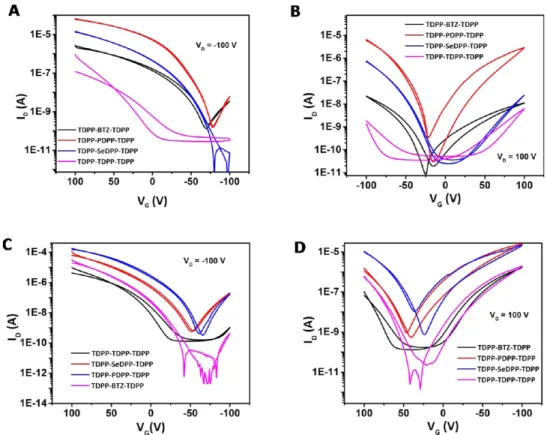
An overview of representative transfer curves (ID−VG) for all materials upon thermal annealing is depicted in Figure 6A,C; the extracted electron and hole mobility values are summarized in Table S2,SI. It is evident that all materials exhibit ambipolar charge transport characteristics. The gate voltage (VG) induced
current modulation under negative as well as positive gate bias leads to changes of the drain current (ID) typically over 3−5 orders of magnitude. The devices demonstrated clear linear and saturation regime transport with negligible hysteresis as exemplified in Figure 6B,D. Overall, the oligomers demon-strated pronounced p-type character compared to its n-type counterpart. The hole mobilities of oligomerfilms were found
to be generally higher than the electron mobilities and range from 6× 10⁻³cm2V−1s−1, for SeDPP, to 6× 10⁻²cm2V−1s−1
for the TDPP−TDPP−TDPP oligomer whereas the electron mobilities range from 10−3and 10−2cm2V−1s−1. The highest electron mobility of close to 10−2cm2V−1s−1was determined
for TDPP−PDPP−TDPP. To understand the role of the
injecting electrodes on the ambipolar nature of the charge transport, transistor characteristics were measured with Au S− D electrodes. Transport parameters measured using Au S−D electrodes are summarized in Table S3,SI. An injection limited behavior is evident in the Au S−D electrodes accompanied by a 1 order of magnitude decrease in theμFETe However, the hole
mobility remains unaffected for most of the oligomers upon comparing the performance of the device fabricated from both Au or Ag electrodes which indicates that the injection barrier significantly modifies the transport levels of electrons compared to the transport levels of holes. Further optimization of the oligomeric transistor was performed with SA by treating the thinfilms with CHCl3vapors. Typical transfer plots for all the
oligomer-based transistors are shown in Figure 7A,B. Interestingly the SAfilms demonstrated comparable or higher μFETe andμFETh than TAfilms.
This opens up the possibility of obtaining high performance ambipolar organic FETs from low temperature processing techniques. Upon thermal annealing of the SA films average μFETe of up to 0.16 cm2/(V s) and hole mobility (μFETh ) of 0.02
cm2/(V s) were obtained with current modulation of up to 105
for TDPP−PDPP−TDPP (Figure 7C,D. Similar enhancement in STAfilms was also observed in other molecules which are
Figure 6.Transfer and output characteristics of thermally annealedfilms obtained from the various oligomer-based thin-film transistors. Panels A and C depict transfer curves (ID−VG) for all oligomers at negative/positive drain voltage (VD). Panels B and D show typical output curves (ID−VD)
for TDPP−TDPP−TDPP-based devices. All TFTs share the same dimensions of channel width (W) and length (L) of 1000 and 30 μm, respectively.
detailed in Table S2,SI. The magnitude of balancedfield-effect mobility in this class of oligomeric systems is one of the best reported to date. A microscopic and macroscopic under-standing of the charge transport can be developed to understand the trends in the transport properties.
Morphological analysis of the samples provides further insight into the difference in the mechanism involved in the charge transport enhancement observed with thermal and solvent annealing. As observed from the AFM images, thermal annealing induces crystallinity to the films with the develop-ment of well-defined crystallites. This enhancement in crystallinity is reflected in higher electron and hole mobilities in the FETs. However, in the case of solvent treatment it is possible that the solvent molecules diffuse to the grain boundaries thereby resulting in soft mixed phases with a
relatively high level of aggregation. Upon thermal annealing of the SAfilms, the morphology is converted into interconnected aggregates, where transport is possible without being hampered by the grain boundaries. Thus, the observed enhancement in the charge transport properties of the DPP oligomers upon combined solvent and thermal treatments can be attributed to formation of interconnected aggregates and the decreased d-spacing and fwhm values responsible for the remarkable device performance. N-channel organic molecules are generally associated with limited air stability due to ease of oxidation originating from low electron affinities. Hence, it is essential to develop molecules which demonstrate considerable air stability. Interestingly in addition, to the excellent charge transport properties of 0.16 cm2/(V s) and ON/OFF ratio exceeding 104,
these oligomers also demonstrate remarkable air stability when
Figure 7.Transfer characteristics obtained from the various oligomer-based thin-film transistors (where, for example, 1E-5 represents 1 × 10⁻⁵). Panels A and B depict transfer curves (ID−VG) for all oligomers after solvent treatment. Panels C and D show typical transfer curves (ID−VG) for all
oligomers after solvent treatment and annealing. All TFTs have the same dimensions of channel width (W) and length (L) of 1000 and 20μm, respectively.
Figure 8.Mobility variation under nitrogen atmosphere and under ambient condition (A; where, for example, 1E-3 represents 1× 10⁻³). Bias stress measurement on TDPP-PDPP-TDPP oligomer-based thin-film transistors with Cytop dielectric layer (B).
the transport measurements were performed in air. It was observed that the devices demonstrated stable operation under ambient operation (RH∼ 20−40% and T ∼ 300 K) for about 1 week (as shown inFigure 8A). Moreover, distinctivefield-effect behavior was retained for the samples even after 4 weeks of exposure to ambient conditions which points to the excellent air stability of the samples to any unwanted oxidation.
Furthermore, bias stability of the best performing FETs was also studied to compare the dielectric−semiconductor interface of these oligomers with other n-channel materials (Figure 8B).
As an example, the best performing TDPP−PDPP−TDPP
molecule was chosen. FETs fabricated with TDPP−PDPP− TDPP demonstrated stable transconductance plots when measured over a time scale of up to 104 s. This level of stability observed in these oligomers toward unwanted oxidation and bias stress is comparable to that of state-of-the-art commercial N2200 polymers which points to the importance of our chemical design principles for realizing stable high performance organic transistors.52
2.9. Theoretical Analysis. In order to scrutinize the
surprising finding that the TDPP−PDPP−TDPP has the
highest electron mobility of the four systems, and to distinguish between the relative impact of intrinsic properties of the oligomers and macroscopic factors such as d-spacing, domain size, and crystalline order on transport properties, the four oligomers were theoretically analyzed at the B3P86/6-31+G* level of theory. The amount of Hartree−Fock exchange in the hybrid functional was increased to 30%.53The effects of solvent were included with the polarized continuum model. Charges were analyzed with the NBO method. UV spectra were calculated with time-dependent density functional theory. All calculations were done with standard methods as implemented in the Gaussian 09 program. Alkyl side chains were replaced by methyl groups. Structure optimizations were carried out without imposing planarity. Reorganization energies were computed from vertical and adiabatic ionization energies and electron affinities in the presence of solvent. Reorganization energies of holes were calculated as IPvert− IPadof the neutral form plus EAad− EAvertof the cation. Reorganization energies
of electrons are EAad− EAvertof the neutral form plus IPvert−
IPad of the anion. The terminal phenyl groups in all four systems are twisted by 26± 1° with respect to the backbone.
Apart from this, TDPP−TDPP−TDPP and TDPP−SeDPP−
TDPP are planar with deviations from planarity of less than 2°. TDPP−BTZ−TDPP is nonplanar only between the BTZ and thienyl units with dihedral angles of 16°. TDPP−PDPP−TDPP has dihedral angles of 35° between the phenyl groups and DPP and of 19° between the phenyl and thienyl rings. Theoretically predicted absorption spectra for the four oligomers are shown in Figure S27,SI. The spectra agree with experiment to within 0.21 eV and reproduce the observed trends. For all systems the lowest energy peak is strongest. TDPP−TDPP−TDPP and TDPP−SeDPP−TDPP have almost identical spectra. TDPP−
BTZ−TDPP and TDPP−PDPP−TDPP absorb at higher
energies (Table S4, SI). Two additional weaker absorptions are found at higher energy. The middle peak at around 2.4−2.5 eV is very weak for the TDPP−PDPP−TDPP and strongest for TDPP−BTZ−TDPP. Absorptions at around 2.3 eV are also visible in the experimental solution spectra of TDPP−TDPP−
TDPP and TDPP−SeDPP−TDPP but are absent for TDPP−
BTZ−TDPP and TDPP−PDPP−TDPP and for all of the thin films. As in the experimental spectra, the third band at around
3.3−3.8 eV is most pronounced for TDPP−PDPP−TDPP.
More than one peak in the absorption spectrum of neutral π-systems is an indication of localization of the charge density54 as it leads to reduced spatial overlap between HOMO and LUMO and reduced oscillator strength of thefirst excited state. The oscillator strength missing in thefirst peak is found in the higher energy absorptions in line with the Thomas−Reiche− Kuhn sum rule.55The sum of the oscillator strengths is about 5 for the three oligomers with only DPP acceptors. The overall smaller oscillator strength of TDPP−BTZ−TDPP is due to the fact that the oligomer is shorter by two thiophene rings. Localization reduces intra- and intermolecular charge transport as overlap between neighbors decreases and reorganization energies increase. The dominance of the first peak in the absorption spectra of the four systems indicates that there is only a little localization but it is stronger for the TDPP−
PDPP−TDPP and TDPP−BTZ−TDPP than for the other
two. Plots of the frontier orbitals of the present systems (Figure S28, SI) reveal that localization occurs not so much on the acceptor but on central versus terminal donor−acceptor blocks. The highest occupied molecular orbital (HOMO) and the lowest unoccupied molecular orbital (LUMO) of TDPP−
TDPP−TDPP and TDPP−SeDPP−TDPP are delocalized over
donor and acceptor and have larger electron density in the center of the molecule. In contrast, the HOMOs of TDPP−
PDPP−TDPP and TDPP−BTZ−TDPP have lower electron
densities toward the middle part of the molecules while the electron density in the LUMOs is highest in the middle. The reason for this is mainly the nonplanarity of these oligomers combined with the weak electron donating power of phenyl and weak accepting power of BTZ in the ground state. The charge transfer character of the strong absorption peaks (oscillator strength > 0.3) was quantified by comparing the charges of the terminal (DPP1) and the central acceptor units (DPP2 and BTZ, respectively) in ground and excited states (Table S5,SI). The data reveal that selenyl are stronger donors than thienyl and phenyl rings and that BTZ is only a very weak acceptor in the ground state. The first excited states (low energy peaks) of TDPP−TDPP−TDPP and TDPP−SeDPP− TDPP do not involve charge transfer; the second and third excited states involve transfer of electron density to the central
part of the molecules. For TDPP−PDPP−TDPP there is
moderate charge transfer to the central part of the molecule in both strong excited states. With BTZ thefirst and the second excited states involve a significant amount of charge transfer to BTZ. Thus, as discussed previously,56,57the acceptor strength of BTZ unfolds only upon excitation. Because hole mobility is influenced by the charge distribution of the valence band (frontier occupied MOs of oligomers) and electron mobility is influenced by the charge distribution of the conduction band (frontier unoccupied MOs), the smallest charges on the acceptor units in ground and excited states would be indicative of the best intrachain hole and electron mobilities, respectively. The strong negative charges in BTZ in the excited states reflect localization of the electrons on BTZ and predict lower electron conductivity. Based on charge distributions increasing mobi-lities are predicted in the order TDPP−SeDPP−TDPP ≈
TDPP−TDPP−TDPP < TDPP−PDPP−TDPP < TDPP−
BTZ−TDPP for holes and TDPP−BTZ−TDPP < TDPP−
SeDPP−TDPP ≈ TDPP−TDPP−TDPP ≈ TDPP−PDPP− TDPP for electrons. Crucial intrinsic parameters for charge carrier mobility are the reorganization energies associated with electron addition or removal. Ionization energies and electron affinities determine the stability of the conducting states and
the alignment of the energy levels with the external contacts. These parameters are collected inTable 2.
Calculated IPs and EAs are larger than the redox potentials (Table 1), but the trends are reproduced correctly. All systems have large EAs around 4 eV, which explains the observed excellent stability of the n-channel materials under ambient conditions. IPs and EAs vary by 0.25 eV among the four systems with TDPP−SeDPP−TDPP having the lowest IP and
largest EA. TDPP−SeDPP−TDPP and TDPP−TDPP−TDPP
have very similar values. TDPP−PDPP−TDPP has the highest IP and lowest EA; BTZ has intermediate IP but a large EA. The reorganization energies of electrons and holes range from 0.18 and 0.26 eV. BTZ has the highest value for holes and only a slightly smaller value than TDPP−PDPP−TDPP for electrons, which is expected as reorganization energies increase with
charge localization. TDPP−SeDPP−TDPP and TDPP−
TDPP−TDPP electrons have smaller reorganization energies
than holes; TDPP−PDPP−TDPP holes have the smaller
reorganization energy. Thus, according to reorganization
energies TDPP−SeDPP−TDPP and TDPP−TDPP−TDPP
are predicted to be the best electron conductors and TDPP− PDPP−TDPP the best hole conductor.
Although all theoretical predictions of molecular parameters are in agreement with experimental data, theory fails to rationalize the question, why is TDPP−PDPP−TDPP the best n-channel material among the four systems? According to their
intrinsic properties TDPP−SeDPP−TDPP and TDPP−
TDPP−TDPP are clearly more promising materials for n-channel transport because both are planar, have the largest EAs, and the smallest reorganization energies for electrons. TDPP− PDPP−TDPP has the smallest EA, its electron reorganization energy is largest among the four oligomers, and it is nonplanar. Because the experimental evidence is exactly the reverse, it must be concluded that macroscopic order which is not addressed with the present calculations plays a decisive role in determining the transport properties. Although intrinsic molecular properties might be less important for oligomers than for polymers, we found no reason why selenyl and thienyl containing oligomers should not be equally good conductors as the phenyl containing ones, and we expect that optimization of
the macroscopic properties of TDPP−SeDPP−TDPP and
TDPP−TDPP−TDPP films will afford even better n-channel materials.
3. CONCLUSIONS
DPP−DPP oligomers exhibit exceptional properties such as air-stable n-channel field-effect behavior, a high degree of solid-state packing, and a broad thin-film absorption extending to near-IR. We have demonstrated that balanced ambipolar mobilities can be achieved by varying the film processing conditions. Annealing has the largest effect on TDPP−PDPP− TDPP probably because of its nonplanar structure. Surprisingly
TDPP−PDPP−TDPP turned out to be the best electron
conductor among the four systems studied, despite optical and electrochemical data showing that it has the lowest EA and the
largest band gap. Moreover, although d-spacing in TDPP− PDPP−TDPP films decreases upon annealing, it remains larger than for the other oligomers and domain sizes are smaller than
for TDPP−TDPP−TDPP and TDPP−SeDPP−TDPP. Since
the only property that is superior for TDPP−PDPP−TDPP is the flat-on orientation, we conclude that electron mobility in these systems requires a high degree of flat-on orientation. Theoretical analysis confirms the trend in optical and electrochemical data and reveals that, in contrast to polymeric materials, transport properties of thienyl, selenyl, and phenyl containing oligomers do not follow established design rules as the nonplanar phenyl system with the lowest EA and the largest reorganization energy for electrons gives rise to the highest electron mobility. Since this is attributed to superior solid-state packing, we expect that optimization of the thienyl and selenyl materials processing will improve their charge transport properties. Remarkable air stability together with facile synthetic methods is the notable feature of this work for construction of optoelectronic devices such as inverters and logical circuits. Although electron mobilities as high as ∼0.2 cm2V−1s−1have been achieved, there is tremendous scope to achieve even higher mobilities by optimizing the annealing conditions for thinfilm.
■
ASSOCIATED CONTENT*
S Supporting InformationThe Supporting Information is available free of charge on the ACS Publications websiteat DOI:10.1021/acsami.6b08453.
Materials and methods, synthesis of DPP−DPP-based oligomers, NMR and mass spectra, theoretical and XRD calculation, thermal properties, UPS, and photophysical studies (PDF)
■
AUTHOR INFORMATIONCorresponding Author *E-mail:[email protected]. Notes
The authors declare no competingfinancial interest.
■
ACKNOWLEDGMENTSS.P. thanks Department of Science and Technology, New Delhi, India for a Swarnajayanti fellowship. S.P., A.S. and R.H.F. would like to acknowledge the funding support through the India-UK APEX-II and UKEIRI Program. Additionally, A.S. and R.H.F. would like to acknowledge the support from EPSRC. T.M. and S.P. thank the Proteomics Facility, Molecular Biophysics Unit, Indian Institute of Science (IISc), for MALDI spectra and NMR Research Centre for NMR facility. T.M. thanks the Indian Institute of Science, Bangalore for a Senior Research Fellowship.
Table 2. Ionization Energies, Electron Affinities, and Reorganization Energies (eV)
oligomers IPvert IPad λh EAvert EAad λe
TDPP−TDPP−TDPP 5.79 5.67 0.247 4.10 4.19 0.187
TDPP−SeDPP−TDPP 5.77 5.65 0.255 4.13 4.22 0.191
TDPP−PDPP−TDPP 6.02 5.93 0.181 3.84 3.97 0.257
TDPP−BTZ−TDPP 5.90 5.76 0.284 4.06 4.20 0.256
■
REFERENCES(1) Xu, Y.; Liu, C.; Khim, D.; Noh, Y. Y. Development of High-Performance Printed Organic Field-Effect Transistors and Integrated Circuits. Phys. Chem. Chem. Phys. 2015, 17, 26553−26574.
(2) Kang, I.; Yun, H. J.; Chung, D. S.; Kwon, S. K.; Kim, Y.-H. Record High Hole Mobility in Polymer Semiconductors via Side-Chain Engineering.J. Am. Chem. Soc. 2013, 135, 14896−14899.
(3) Di Pietro, R.; Fazzi, D.; Kehoe, T. B.; Sirringhaus, H. Spectroscopic Investigation of Oxygen- and Water-Induced Electron Trapping and Charge Transport Instabilities in n-type Polymer Semiconductors. J. Am. Chem. Soc. 2012,134, 14877−14889.
(4) Zhong, H.; Smith, J.; Rossbauer, S.; White, A. J. P.; Anthopoulos, T. D.; Heeney, M. Air-Stable and High-Mobility n-Channel Organic Transistors Based on Small-Molecule/Polymer Semiconducting Blends.Adv. Mater. 2012, 24, 3205−3211.
(5) Fabiano, S.; Usta, H.; Forchheimer, R.; Crispin, X.; Facchetti, A.; Berggren, M. Selective Remanent Ambipolar Charge Transport in Polymeric Field-Effect Transistors For High-Performance Logic Circuits Fabricated in Ambient. Adv. Mater. 2014,26, 7438−7443.
(6) Yun, H. J.; Choi, H. H.; Kwon, S. K.; Kim, Y. H.; Cho, K. Conformation-Insensitive Ambipolar Charge Transport in a Diketo-pyrrolopyrrole-Based Co-polymer Containing Acetylene Linkages. Chem. Mater. 2014, 26, 3928−3937.
(7) Meager, I.; Nikolka, M.; Schroeder, B. C.; Nielsen, C. B.; Planells, M.; Bronstein, H.; Rumer, J. W.; James, D. I.; Ashraf, R. S.; Sadhanala, A.; Hayoz, P.; Flores, J.-C.; Sirringhaus, H.; McCulloch, I. Thieno[3,2-b]thiophene Flanked Isoindigo Polymers for High Performance Ambipolar OFET Applications. Adv. Funct. Mater. 2014, 24, 7109− 7115.
(8) Di, C. -a.; Liu, Y.; Yu, G.; Zhu, D. Interface Engineering: An Effective Approach toward High-Performance Organic Field-Effect Transistors. Acc. Chem. Res. 2009, 42, 1573−1583.
(9) Beaujuge, P. M.; Fréchet, J. M. J. Molecular Design and Ordering Effects in π-Functional Materials for Transistor and Solar Cell Applications. J. Am. Chem. Soc. 2011, 133, 20009−20029.
(10) Fan, J.; Yuen, J. D.; Wang, M.; Seifter, J.; Seo, J. H.; Mohebbi, A. R.; Zakhidov, D.; Heeger, A.; Wudl, F. High-Performance Ambipolar Transistors and Inverters from an Ultralow Bandgap Polymer. Adv. Mater. 2012, 24, 2186−2190.
(11) Chen, Z.; Lee, M. J.; Shahid Ashraf, R.; Gu, Y.; Albert-Seifried, S.; Meedom Nielsen, M.; Schroeder, B.; Anthopoulos, T. D.; Heeney, M.; McCulloch, I.; Sirringhaus, H. High-Performance Ambipolar Diketopyrrolopyrrole-Thieno[3,2-b]thiophene Copolymer Field-Effect Transistors with Balanced Hole and Electron Mobilities. Adv. Mater. 2012, 24, 647−652.
(12) Gruber, M.; Jung, S. H.; Schott, S.; Venkateshvaran, D.; Kronemeijer, A. J.; Andreasen, J. W.; McNeill, C. R.; Wong, W. W. H.; Shahid, M.; Heeney, M.; Lee, J. K.; Sirringhaus, H. Enabling High-Mobility, Ambipolar Charge-Transport in a DPP-benzotriazole Copolymer by Side-Chain Engineering. Chem. Sci. 2015, 6, 6949− 6960.
(13) Gibson, G. L.; Gao, D.; Jahnke, A. A.; Sun, J.; Tilley, A. J.; Seferos, D. S. Molecular Weight and End Capping Effects on the Optoelectronic Properties of Structurally Related ’Heavy Atom’ Donor-Acceptor Polymers. J. Mater. Chem. A 2014, 2, 14468−14480. (14) Liu, S.-Y.; Liu, W. Q.; Xu, J. Q.; Fan, C. C.; Fu, W. F.; Ling, J.; Wu, J. Y.; Shi, M. M.; Jen, A. K. Y.; Chen, H. Z. Pyrene and Diketopyrrolopyrrole-Based Oligomers Synthesized via Direct Aryla-tion for OSC ApplicaAryla-tions. ACS Appl. Mater. Interfaces 2014, 6, 6765− 6775.
(15) Li, Y.; Sonar, P.; Murphy, L.; Hong, W. High Mobility Diketopyrrolopyrrole (DPP)-Based Organic Semiconductor Materials for Organic Thin Film Transistors and Photovoltaics. Energy Environ. Sci. 2013, 6, 1684−1710.
(16) Głowacki, E. D.; Coskun, H.; Blood-Forsythe, M. A.; Monkowius, U.; Leonat, L.; Grzybowski, M.; Gryko, D.; White, M. S.; Aspuru-Guzik, A.; Sariciftci, N. S. Hydrogen-Bonded Diketopyrro-lopyrrole (DPP) Pigments as Organic Semiconductors. Org. Electron. 2014, 15, 3521−3528.
(17) Qiao, Y.; Guo, Y.; Yu, C.; Zhang, F.; Xu, W.; Liu, Y.; Zhu, D. Diketopyrrolopyrrole-Containing Quinoidal Small Molecules for High-Performance, Air-Stable, and Solution-Processable n-Channel Organic Field-Effect Transistors. J. Am. Chem. Soc. 2012, 134, 4084− 4090.
(18) Fabiano, S.; Braun, S.; Fahlman, M.; Crispin, X.; Berggren, M. Effect of Gate Electrode Work-Function on Source Charge Injection in Electrolyte-Gated Organic Field-Effect Transistors.Adv. Funct. Mater. 2014, 24, 695−700.
(19) Lee, J.; Han, A. R.; Yu, H.; Shin, T. J.; Yang, C.; Oh, J. H. Boosting the Ambipolar Performance of Solution-Processable Polymer Semiconductors via Hybrid Side-Chain Engineering. J. Am. Chem. Soc. 2013, 135, 9540−9547.
(20) Kanimozhi, C.; Yaacobi-Gross, N.; Chou, K. W.; Amassian, A.; Anthopoulos, T. D.; Patil, S. Diketopyrrolopyrrole−Diketopyrrolo-pyrrole-Based Conjugated Copolymer for High-Mobility Organic Field-Effect Transistors.J. Am. Chem. Soc. 2012, 134, 16532−16535.
(21) Senanayak, S. P.; Ashar, A. Z.; Kanimozhi, C.; Patil, S.; Narayan, K. S. Room-Temperature Bandlike Transport and Hall effect in a High-Mobility Ambipolar Polymer. Phys. Rev. B: Condens. Matter Mater. Phys. 2015, 91, 115302DOI: 10.1103/PhysRevB.91.115302.
(22) Dhar, J.; Kanimozhi, C.; Yaccobi-Gross, N.; Anthopoulos, T. D.; Salzner, U.; Patil, S. Selenium in Diketopyrrolopyrrole-Based Polymers: Influence on Electronic Properties and Charge Carrier Mobilities.Isr. J. Chem. 2014, 54, 817−827.
(23) Dhar, J.; Mukhopadhay, T.; Yaacobi-Gross, N.; Anthopoulos, T. D.; Salzner, U.; Swaraj, S.; Patil, S. Effect of Chalcogens on Electronic and Photophysical Properties of Vinylene-Based Diketopyrrolopyrrole Copolymers. J. Phys. Chem. B 2015, 119, 11307−11316.
(24) Sun, B.; Hong, W.; Yan, Z.; Aziz, H.; Li, Y. Record High Electron Mobility of 6.3 cm2V−1s−1 Achieved for Polymer Semi-conductors Using a New Building Block. Adv. Mater. 2014, 26, 2636− 2642.
(25) Lin, H. W.; Lee, W. Y.; Chen, W. C. Selenophene-DPP Donor-Acceptor Conjugated Polymer for High Performance Ambipolar Field Effect Transistor and Nonvolatile Memory Applications. J. Mater. Chem. 2012, 22, 2120−2128.
(26) Kang, I.; An, T. K.; Hong, J. a.; Yun, H. J.; Kim, R.; Chung, D. S.; Park, C. E.; Kim, Y. H.; Kwon, S. K. Effect of Selenophene in a DPP Copolymer Incorporating a Vinyl Group for High-Performance Organic Field-Effect Transistors. Adv. Mater. 2013, 25, 524−528.
(27) Lin, H. W.; Lee, W. Y.; Chen, W. C. Selenophene-DPP Donor-Acceptor Conjugated Polymer for High Performance Ambipolar Field Effect Transistor and Nonvolatile Memory Applications. J. Mater. Chem. 2012, 22, 2120−2128.
(28) Yuan, Y.; Giri, G.; Ayzner, A. L.; Zoombelt, A. P.; Mannsfeld, S. C. B.; Chen, J.; Nordlund, D.; Toney, M. F.; Huang, J.; Bao, Z. Ultra-High Mobility Transparent Organic Thin Film Transistors Grown by an Off-Centre Spin-Coating Method. Nat. Commun. 2014, 5, 3005 DOI: 10.1038/ncomms4005.
(29) Ullah Khan, H.; Li, R.; Ren, Y.; Chen, L.; Payne, M. M.; Bhansali, U. S.; Smilgies, D.-M.; Anthony, J. E.; Amassian, A. Solvent Vapor Annealing in the Molecular Regime Drastically Improves Carrier. ACS Appl. Mater. Interfaces 2013, 5, 2325−2330.
(30) Wei, Q.; Mukaida, M.; Naitoh, Y.; Ishida, T. Morphological Change and Mobility Enhancement in PEDOT: PSS by Adding Co-solvents. Adv. Mater. 2013, 25, 2831−2836.
(31) Kanimozhi, C.; Naik, M.; Yaacobi-Gross, N.; Burnett, E. K.; Briseno, A. L.; Anthopoulos, T. D.; Patil, S. Controlling Conformations of Diketopyrrolopyrrole-Based Conjugated Polymers: Role of Torsional Angle. J. Phys. Chem. C 2014, 118, 11536−11544.
(32) Wijsboom, Y. H.; Patra, A.; Zade, S. S.; Sheynin, Y.; Li, M.; Shimon, L. J. W.; Bendikov, M. Controlling Rigidity and Planarity in Conjugated Polymers: Poly(3,4-ethylenedithioselenophene). Angew. Chem., Int. Ed. 2009, 48, 5443−5447.
(33) Henson, Z. B.; Mullen, K.; Bazan, G. C. Design Strategies for Organic Semiconductors Beyond the Molecular Formula. Nat. Chem. 2012, 4, 699−704.
(34) Noriega, R.; Rivnay, J.; Vandewal, K.; Koch, F. P. V.; Stingelin, N.; Smith, P.; Toney, M. F.; Salleo, A. A General Relationship between Disorder, Aggregation and Charge Transport in Conjugated Polymers. Nat. Mater. 2013, 12, 1038−1044.
(35) Liu, S.-Y.; Shi, M. M.; Huang, J. C.; Jin, Z.-N.; Hu, X. L.; Pan, J. Y.; Li, H. Y.; Jen, A. K. Y.; Chen, H. Z. C-H Activation: Making Diketopyrrolopyrrole Derivatives Easily Accessible. J. Mater. Chem. A 2013, 1, 2795−2805.
(36) Lin, Y.; Zhan, X. Oligomer Molecules for Efficient Organic Photovoltaics. Acc. Chem. Res. 2016, 49, 175−183.
(37) Zhang, Q. T.; Tour, J. M. Alternating Donor/Acceptor Repeat Units in Polythiophenes. Intramolecular Charge Transfer for Reducing Band Gaps in Fully Substituted Conjugated Polymers.J. Am. Chem. Soc. 1998, 120, 5355−5362.
(38) Planells, M.; Schroeder, B. C.; McCulloch, I. Effect of Chalcogen Atom Substitution on the Optoelectronic Properties in Cyclopentadithiophene Polymers. Macromolecules 2014, 47, 5889− 5894.
(39) Fringuelli, F.; Marino, G.; Taticchi, A.; Grandolini, G. A Comparative Study of the Aromatic Character of Furan, Thiophen, Selenophen, and Tellurophen. J. Chem. Soc., Perkin Trans. 2 1974, 332−337.
(40) Hollinger, J.; Gao, D.; Seferos, D. S. Selenophene Electronics. Isr. J. Chem. 2014, 54, 440−453.
(41) Shahid, M.; McCarthy-Ward, T.; Labram, J.; Rossbauer, S.; Domingo, E. B.; Watkins, S. E.; Stingelin, N.; Anthopoulos, T. D.; Heeney, M. Low Band Gap Selenophene-Diketopyrrolopyrrole Polymers Exhibiting High and Balanced Ambipolar Performance in Bottom-Gate Transistors. Chem. Sci. 2012, 3, 181−185.
(42) Breuer, T.; Celik, M. A.; Jakob, P.; Tonner, R.; Witte, G. Vibrational Davydov Splittings and Collective Mode Polarizations in Oriented Organic Semiconductor Crystals.J. Phys. Chem. C 2012, 116, 14491−14503.
(43) Chau, L. K.; England, C. D.; Chen, S.; Armstrong, N. R. Visible Absorption and Photocurrent Spectra of Epitaxially Deposited Phthalocyanine Thin Films: Interpretation of Exciton Coupling Effects.J. Phys. Chem. 1993, 97, 2699−2706.
(44) DiCésare, N.; Belletête, M.; Marrano, C.; Leclerc, M.; Durocher, G. Intermolecular Interactions in Conjugated Oligothiophenes. 1. Optical Spectra of Terthiophene and Substituted Terthiophenes Recorded in Various Environments.J. Phys. Chem. A 1999, 103, 795− 802.
(45) Bässler, H.; Köhler, A. Charge Transport in Organic Semiconductors. In Unimolecular and Supramolecular Electronics I: Chemistry and Physics Meet at Metal-Molecule Interfaces; Metzger, M. R., Ed.; Springer: Berlin, Heidelberg, 2012; pp 1−65, DOI: 10.1007/ 128_2011_218.
(46) Gregg, B. A. Evolution of Photophysical and Photovoltaic Properties of Perylene Bis(phenethylimide) Films Upon Solvent Vapor Annealing. J. Phys. Chem. 1996, 100, 852−859.
(47) Dickey, K. C.; Anthony, J. E.; Loo, Y. L. Improving Organic Thin-Film Transistor Performance through Solvent-Vapor Annealing of Solution-Processable Triethylsilylethynyl Anthradithiophene. Adv. Mater. 2006, 18, 1721−1726.
(48) Bleiholder, C.; Gleiter, R.; Werz, D. B.; Köppel, H. Theoretical Investigations on Heteronuclear Chalcogen−Chalcogen Interactions: On the Nature of Weak Bonds between Chalcogen Centers. Inorg. Chem. 2007, 46, 2249−2260.
(49) Chung, H.; Diao, Y. Polymorphism as an Emerging Design Strategy for High Performance Organic Electronics. J. Mater. Chem. C 2016, 4, 3915−3933.
(50) Dhar, J.; Venkatramaiah, N.; A, A.; Patil, S. Photophysical, Electrochemical and Solid State Properties of Diketopyrrolopyrrole-Based Molecular Materials: Importance of the Donor Group. J. Mater. Chem. C 2014, 2, 3457−3466.
(51) Di, C. a.; Lu, K.; Zhang, L.; Liu, Y.; Guo, Y.; Sun, X.; Wen, Y.; Yu, G.; Zhu, D. Solvent-Assisted Re-annealing of Polymer Films for Solution-Processable Organic Field-Effect Transistors. Adv. Mater. 2010, 22, 1273−1277.
(52) Chen, Z.; Zheng, Y.; Yan, H.; Facchetti, A. Naphthalenedi-carboximide- vs PerylenediNaphthalenedi-carboximide-Based Copolymers. Synthesis and Semiconducting Properties in Bottom-Gate N-Channel Organic Transistors. J. Am. Chem. Soc. 2009, 131, 8−9.
(53) Salzner, U.; Pickup, P. G.; Poirier, R. A.; Lagowski, J. B. Accurate Method for Obtaining Band Gaps in Conducting Polymers Using a DFT/Hybrid Approach. J. Phys. Chem. A 1998, 102, 2572−2578.
(54) Salzner, U.; Aydin, A. Improved Prediction of Properties of π-Conjugated Oligomers with Range-Separated Hybrid Density Func-tionals. J. Chem. Theory Comput. 2011, 7, 2568−2583.
(55) Izuyama, T. The Thomas-Kuhn Sum Rule and Superfluidity. I: Applicability of Linear Response Theory to Macroscopic Systems. Prog. Theor. Phys. 1976, 56, 1674−1688.
(56) Salzner, U. Effect of Donor−Acceptor Substitution on Optoelectronic Properties of Conducting Organic Polymers. J. Chem. Theory Comput. 2014, 10, 4921−4937.
(57) Levitin, M.; Parnovski, L. Commutators, Spectral Trace Identities, and Universal Estimates for Eigenvalues. J. Funct. Anal. 2002, 192, 425−445.