COMPENSATION OF MUTUAL COUPLING IN
TRANSMITTING ARRAYS OF THIN WIRE
ANTENNAS
a thesis submitted to
the graduate school of
engineering and natural sciences
of istanbul medipol university
in partial fulfillment of the requirements for
the degree of
master of science
in
electrical, electronics engineering and cyber systems
By
Sana Khan
August, 2017
ABSTRACT
COMPENSATION OF MUTUAL COUPLING IN
TRANSMITTING ARRAYS OF THIN WIRE ANTENNAS
Sana Khan
M.S. in Electrical, Electronics Engineering and Cyber Systems Advisor: Prof. Dr. Erc¨umend Arvas
August, 2017
In the classical approach of antenna array theory, mutual coupling between elements is usu-ally ignored. However, depending on the application, errors due to mutual coupling can be significant. This thesis presents a numerical study for the compensation of mutual cou-pling between elements in small dipole arrays using Method of Moment. By using the mutual impedance of the antenna elements, it is possible to compute a new set of excitation voltages. Using these new compensated voltages one can obtain the pattern that would be similar to the pattern obtained by the original voltages if there were no mutual coupling. This compen-sated pattern is compared with the radiation pattern obtained using pattern multiplication method which does not include mutual coupling. In this thesis, mutual coupling has been compensated for different array configurations including linear arrays, circular arrays as well as 3-Dimensional arrays. Individual element of the arrays can have different length, radius and relative positions in space.
Keywords: Method of Moments, Mutual Coupling Compensation, Linear Arrays, Planar Arrays, 3-Dimensional Arrays, Arrays of Dipoles.
¨
OZET
VER˙IC˙I ˙INCE TEL ANTEN D˙IZ˙ILER˙INDE KARS
¸ILIKLI
BA ˘
GLANMANIN TAZM˙IN ED˙ILMES˙I
Sana Khan
Elektrik Elektronik M¨uhendisli˘gi ve Siber Sistemler, Y¨uksek Lisans Tez Danı¸smanı: Prof. Dr. Erc¨umend Arvas
A˘gustos, 2017
Anten dizisi teorisinin klasik yakla¸sımında, ¨o˘geler arasındaki kar¸sılıklı ba˘glanma genellikle dikkate alınmaz. Bununla birlikte, uygulamaya ba˘glı olarak, kar¸sılıklı ba˘glantıdan kay-naklanan hatalar ¨onemli olabilir. Bu tez, Moment Metodu’nu kullanarak k¨u¸c¨uk dipol dizilerindeki elemanlar arasındaki kar¸sılıklı ba˘gın tazmini i¸cin sayısal bir ¸calı¸sma sunmak-tadır. Anten elemanlarının kar¸sılıklı empedansını kullanarak yeni bir uyartım gerilimi seti hesaplamak m¨umk¨und¨ur. Bu yeni dengelenmi¸s gerilimleri kullanarak, kar¸sılıklı bir ba˘glanma olmasaydı orijinal gerilimlerle elde edilen desene benzer bir model elde edebilir. Bu den-gelenmi¸s desen, kar¸sılıklı e¸sle¸sme i¸cermeyen ¸carpma metodu deseni kullanılarak elde edilen radyasyon deseni ile kar¸sıla¸stırılır. Bu dengelenmi¸s desen, kar¸sılıklı e¸sle¸sme i¸cermeyen ¸carpma metodu deseni kullanlarak elde edilen radyasyon deseni ile kar¸sıla¸stırılır. Bu tezde, kar¸sılıklı ba˘glantı, do˘grusal diziler, dairesel diziler ve 3 Boyutlu diziler de dahil olmak ¨uzere farklı dizi yapılandırmaları i¸cin telafi edilmi¸stir. Dizilerin bireysel elemanları, uzaydaki farklı uzunluk, yarı¸cap ve g¨oreli konumlara sahip olabilir.
Acknowledgement
I am grateful to my advisor Prof. Dr. Erc¨umend Arvas for his relentless efforts in guiding me and enabling me to take up this endeavor. Despite my shortcomings he never gave up on me. Thank you Sir.
I am thankful to my parents for letting me earn my dreams...My family and friends who always instilled hope in me in gloomy days. Last but not the least, I am thankful to my husband who has stood besides me through this whole journey.
I am thankful to Turkey (TUBITAK) as this thesis was partially supported by it under the project number 215E316.
vii
Contents
1 Introduction 1
1.1 Motivation . . . 4
1.2 Approach . . . 8
1.3 Overview . . . 9
2 Methods of Computational Electromagnetics (CEM) 11 2.1 Low-Frequency Methods . . . 13
2.1.1 Finite Difference Time Domain Method . . . 13
2.1.2 Finite Element Method . . . 14
2.1.3 Method of Moments . . . 14
2.2 High-Frequency Methods . . . 14
2.2.1 Uniform Theory of Diffraction (UTD) . . . 15
2.2.2 Geometrical Optics (GO) . . . 15
2.2.3 Physical Theory of Diffraction (PTD) . . . 15
CONTENTS ix
2.4 Dipoles . . . 17
2.4.1 Single Dipole in Free Space . . . 17
2.5 Array Theory . . . 20
2.6 Compensation Method . . . 22
2.7 Formulation of Matlab Code . . . 25
3 Simulations and Results 26 3.1 Identical Arrays . . . 26
3.1.1 Mutual Impedance . . . 26
3.1.2 Mutual Coupling Compensation . . . 33
3.2 Non-Identical Arrays . . . 40
3.2.1 Mutual Impedance . . . 40
3.2.2 Mutual Coupling Compensation . . . 43
3.3 Compensation of Circular Arrays . . . 55
3.3.1 Square Array . . . 55
3.3.2 Triangular Array . . . 59
3.4 Compensation of 3-Dimensional Circular Arrays . . . 62
3.5 Comparison with commercial software . . . 65
CONTENTS x
Appendix B Formulation of the Z matrix for N-segment solution 82
List of Figures
1.1 Circular array of four half-wave dipoles with radius of circle λ/4. a) Side View. b) Top View. . . 4 1.2 Four isotropic sources arranged in a circular array. . . 5 1.3 Theoretical pattern of the circular array of four dipoles calculated by pattern
multiplication method. . . 6 1.4 The real practical pattern of circular array of four dipoles. . . 7 1.5 Radiation pattern of a circular array of four dipoles. . . 8
2.1 A flow chart showing different computational electromagnetic techniques. . . 13 2.2 Normalized E-plane pattern of a half-wave dipole. . . 18 2.3 Normalized H-plane pattern of a half-wave dipole. . . 19 2.4 Magnitude and phase of the current distribution for a center-fed dipole in free
space with length L = 0.4781λ, radius a = λ/1000 and number of expansion functions N P = 63. . . 20 2.5 Equally spaced linear array of isotropic point sources [1]. . . 21 2.6 Equivalent circuit of N antennas with no mutual coupling . . . 22
LIST OF FIGURES xii
3.1 Two parallel dipole antennas in non-staggered arrangement with length L = 0.4781λ, radius a = 0.001λ, separation d/λ, and λ = 1 m. . . 27 3.2 Real part of mutual impedance between two parallel dipole antennas as a
function of spacing relative to wavelength with L = 0.4781λ and a = 0.001λ. Geometry shown in Fig. 3.1 . . . 27 3.3 Imaginary part of mutual impedance between two parallel dipole antennas as
a function of spacing relative to wavelength with L = 0.4781λ and a = 0.001λ. Geometry shown in Fig. 3.1. . . 28 3.4 Two identical parallel dipole antennas in staggered arrangement with length
L = 0.4781λ, radius a = 0.001λ, fixed horizontal separation of 0.25λ, and staggered by h/λ. . . 29 3.5 Real part of mutual impedance between two identical but staggered dipole
antennas of length L = 0.4781λ, radius a = 0.001λ, fixed horizontal separation of 0.25λ, and staggered by h/λ. . . 30 3.6 Imaginary part of mutual impedance between two identical but staggered
dipole antennas of length L = 0.4781λ, radius a = 0.001λ, fixed horizontal separation of 0.25λ, and staggered by h/λ. . . 30 3.7 Two dipole antennas in collinear arrangement as a function of spacing relative
to wavelength with length L = 0.4781λ and radius a = 0.001λ. . . 31 3.8 Real part of mutual impedance between two collinear dipole antennas as a
function of spacing relative to wavelength with length L = 0.4781λ and radius a = 0.001λ. . . 32 3.9 Imaginary part of mutual impedance between two collinear dipole antennas
as a function of spacing relative to wavelength with length L = 0.4781λ and radius a = 0.001λ. . . 32 3.10 Two parallel antennas of length λ/2 with a = λ/200. . . 33
LIST OF FIGURES xiii
3.11 Radiation patterns for two parallel dipole antennas with different element separations. (a) d = 0.1λ (b) d = 0.2λ (c) d = 0.3λ (d) d = 0.4λ (e) d = 0.5λ. 36 3.12 Five dipole antennas of length λ/2, a = λ/200 and spacing d. . . 37 3.13 Radiation pattern for five-element dipole array with separation d = 0.5λ and
main-beam direction ϕ = 45◦. . . 38 3.14 Radiation pattern for five-element dipole array with separation d = 0.3λ and
main-beam direction ϕ = 60◦. . . 39 3.15 Two parallel dipole antennas in non-staggered arrangement of lengths λ/2
and λ/3 as a function of spacing relative to wavelength with radius a = 0.001λ. 40 3.16 Mutual impedance curves between two parallel antennas in non-staggered
ar-rangement of lengths λ/2 and λ/3 as a function of spacing relative to wave-length with a = 0.001λ. . . 41 3.17 Two parallel dipole antennas of lengths λ/2 and λ/3 in staggered arrangement
as a function of spacing relative to wavelength with a = 0.001λ, horizontal separation d and staggered by h = λ/4. . . 41 3.18 Mutual impedance curves between two parallel antennas of lengths λ/2 and
λ/3 with a = 0.001λ, staggered by h = λ/4. . . 42 3.19 Two antennas of lengths λ/2 and λ/3 in collinear arrangement as a function
of spacing relative to wavelength with radius a = 0.001λ. . . 42 3.20 Mutual impedance curves for two dipole antennas of lengths λ/2 and λ/3 in
a collinear arrangement with radius a = 0.001λ. . . 43 3.21 Two parallel antennas in non-staggered arrangement of lengths λ/2 and λ/3
as a function of spacing relative to wavelength with radius a = 0.001λ, and separation d. . . 44
LIST OF FIGURES xiv
3.22 Radiation pattern of two-elements non-identical non-staggered dipoles with different element separations. (a) d = 0.1λ (b) d = 0.2λ (c) d = 0.3λ (d) d = 0.4λ (e) d = 0.5λ. . . 47 3.23 Two parallel dipole antennas of lengths λ/2 and λ/3 in staggered arrangement
as a function of spacing relative to wavelength with radius a = 0.001λ, and staggered by h = λ/4. . . 48 3.24 Radiation pattern of two-element non-identical staggered dipoles with
differ-ent elemdiffer-ent separations. (a) d = 0.1λ (b) d = 0.2λ (c) d = 0.3λ (d) d = 0.4λ (e) d = 0.5λ. . . 51 3.25 Two antennas of lengths λ/2 and λ/3 in collinear arrangement as a function
of spacing relative to wavelength with a = 0.001λ. . . 52 3.26 Three staggered dipole antennas of different lengths L1 = λ/2, L2 = λ/4,
L3 = λ/3. . . 53
3.27 Radiation pattern of three element staggered array in xy-plane at 300 MHz. 53 3.28 Radiation pattern of three element staggered array in yz-plane at 300 MHz. 54 3.29 Radiation pattern of three element staggered array in xz-plane at 300 MHz. 54 3.30 Circular array of four half-wave dipoles with radius of circle λ/4. a) Side view.
b) Top view. . . 55 3.31 Radiation pattern of four element circular array in XY plane at 300 MHz with
uniform excitation. . . 56 3.32 Current distribution of the four dipole array when all antennas are uniformly
excited. . . 57 3.33 Radiation pattern of four element circular array in XY plane at 300 MHz with
LIST OF FIGURES xv
3.34 Current distribution of the four dipole array when antennas are excited with a progressive phase. . . 59 3.35 Triangular array of three dipole antennas. a) Side view. b) Top view. . . 60 3.36 Radiation pattern of three element triangular array in xy-plane at 300 MHz
with uniform excitation. . . 61 3.37 Radiation pattern of three element triangular array in XY plane at 300MHz
with progressive phase excitation. . . 62 3.38 Three-dimensional dipole array with seven elements. Four dipoles are placed
along a circle of radius 0.5λ and three dipoles along a radius of 0.4λ which are displaced in the z-axis by h = λ/4. . . 63 3.39 Radiation pattern in xy-plane for a 3-Dimensional dipole array at 300 MHz. 64 3.40 Radiation pattern in yz-plane for a 3-Dimensional dipole array at 300 MHz. 64 3.41 Radiation pattern in xz-plane for a 3-Dimensional dipole array at 300 MHz. 65 3.42 Radiation pattern comparison of HFSS and MATLAB in xy-plane for a
3-Dimensional dipole array at 300 MHz with mutual coupling. . . 66 3.43 Radiation pattern comparison of HFSS and MATLAB in yz-plane for a
3-Dimensional dipole array at 300 MHz with mutual coupling. . . 66 3.44 Radiation pattern comparison of HFSS and MATLAB in xz-plane for a
3-Dimensional dipole array at 300 MHz with mutual coupling. . . 67 3.45 Circular array of four dipole elements in HFSS. . . 68 3.46 Radiation pattern comparison of HFSS and MATLAB in xy-plane for a square
array excited with uniform phase progression operating at 300 MHz with mutual coupling. . . 68
LIST OF FIGURES xvi
3.47 Compensated radiation patterns comparison of HFSS and MATLAB in xy-plane for a square array excited with uniform phase progression operating at 300 MHz. . . 69 3.48 Mean Square Error for the compensation of circular array of four dipoles. . . 70
A.1 A wire scatterer of length L and radius a illuminated by an incident plane wave. 75 A.2 Surface equivalence model with equivalent surface current density Js in free
space. . . 76 A.3 Equivalent filamentary line source for a z-directed wire when wire radius a λ
[1]. . . 77 A.4 Expansion functions. a)“Staircase” approximation to an actual current
dis-tribution. b) Set of overlapping triangular functions. c) Set of overlapping piecewise sinusoidal functions [1]. . . 79 A.5 Piecewise sinusoidal expansion function [1]. . . 80
B.1 Wire segment along z-axis [2]. . . 82
C.1 a) Coaxial line feeding a monopole through a ground plane. b) Mathematical model of (a) [1]. . . 86
List of Tables
3.1 Compensation voltages Vs10 and Vs20 for the two element dipole array for dif-ferent element separations. . . 36 3.2 Compensation voltages for the five-element dipole array with different
inter-element separations d and main-beam directions ϕ. . . 38 3.3 Excitation voltages for the five-element dipole array with different
inter-element separations d and main-beam directions ϕ. . . 39 3.4 Compensation voltages Vs10 and Vs20 of two-element non-identical non-staggered
dipole array for different antenna separations. . . 44 3.5 Compensation voltages Vs10 and Vs20 for two-elements non-identical staggered
dipole array for different antenna separations. . . 48 3.6 Compensation voltages Vs10 and Vs20 of two-element non-identical collinear
Chapter 1
Introduction
Antenna arrays have a wide range of applications involving commercial and military ap-plications [1],[3]. They are used in systems such as radio, television broadcasting, weather research, radar, missile guidance systems and space communications. Due to miniaturization of electronic devices, small-sized antenna arrays also called as compact antenna arrays has attracted a lot of interest. One such example of compact antenna arrays is called Multiple Input Multiple Output (MIMO) system. In conventional wireless communications, a single main antenna was used to transmit and receive data. Nowadays, mobile phones or smart phones provide us with multiple services. These services include GPS, WiFi, Bluetooth, In-frared etc. All of these services require an antenna in order to receive and transmit data. In the current industry, the single main antenna has been evolved to multiantenna solution as MIMO. In a MIMO system these multiple antennas are placed at a close proximity inside the handset. Due to the small distance between the antenna elements they interact with one an-other. This electromagnetic interaction is called mutual coupling. This interaction changes the current magnitude, phase, and distribution on each element from their free space values. As a consequence, total array pattern is altered. Compact antenna arrays suffer from mu-tual coupling which can alter the overall radiation pattern, gain, bandwidth and impedance matching of the antenna. Mutual coupling between the antenna elements in an antenna array is a classic problem which is responsible for the degradation of array performance [4], [5], [6]. In the classical array theory, it is often taken that the radiation pattern of an array of identical antenna elements is the product of an element pattern and an array factor. The element pattern is the pattern of an isolated element with center usually at origin. This element is assumed to be excited by a unit voltage. The array factor is a sum of fields from
isotropic point sources located at center of each array element and is found from the element voltages (amplitudes and phases) and their locations [1]. Therefore, in the classical array theory, it is assumed that all the elements of the array have equal radiation pattern, in other words, the coupling between individual elements is ignored. For a practical array, this is not entirely true since mutual coupling causes each element to see a different environment and consequently has a different radiation pattern from its neighboring elements. Several techniques to reduce mutual coupling and improve the isolation have been investigated [7], [8]. Some of them are given below:
Decoupling Networks (DN): These networks use lumped elements and hybrid cou-plers to reduce mutual coupling. It has a disadvantage of narrow bandwidth. Parallel resonant circuits can be used to achieve broad bandwidth. Strips and slots introduce different resonances at different frequencies to help increase the isolation.
Defected Ground Plane Structure (DGS): In this technique ground plane is modified by introducing slits of different shapes. This modification creates a band-stop filter and suppresses the coupling fields.
Parasitic Elements: Inductance and capacitance is introduced using Electromagnetic Band Gap (EBG) to create a forbidden band of frequencies which helps in isolation of the antennas.
Meta-materials: These are materials with special properties, e.g., negative permit-tivity or permeability or both. They are used due to existence of band gaps in their frequency response. The band gaps act as band notch filters and destroy mutual cou-pling between the elements. Mostly used structures are split ring resonators (SRR) and complementary split ring resonators (CSRR). Due to the substrate there is a de-terioration of bandwidth.
Neutralization Lines (NL): In this technique current at the input element is taken at a location where impedance is minimum and current is maximum and then its phase is reversed by choosing suitable length of NL. The reversed current is then fed to nearby antenna to lessen the amount of coupled current. This method has a narrow bandwidth and the location of maximum current is difficult to find.
elements or special materials may be needed to reduce the coupling. This dissertation uses a non-invasive method in which the physical structure or design of the antenna is not changed. Neither any special materials or elements are required. Instead, only the excitation voltages of the antenna are changed and these new excitation voltages which are called compensated voltages produce a radiation pattern which is very similar to the pattern obtained from pattern multiplication method. In summary, the array factor method gives us the theoretical pattern of antenna arrays without mutual coupling. The real practical pattern is different from the theoretical pattern because of mutual coupling. In order to make the real practical pattern similar to our desired theoretical pattern, we compensate for the mutual coupling.
This thesis considers arrays of thin wire dipole antennas with length less than or equal to λ/2. Such antennas are usually called as single mode antennas. The individual elements in the array may not be identical in length, radius or position. A number of methods have been suggested for the compensation of mutual coupling [6], [9] and [10]. Here a numerical method has been used to compensate for mutual coupling, called Method of Moments (MoM). By using thin wire approximation the exact integral equation is solved approximately using MoM which helps us to compute the current distribution on the thin wire antennas. This gives us the radiation pattern in the presence of mutual coupling. Using the moment matrix for the array, we can calculate the coupling effect in terms of scattering matrix which is then used to find the new input voltages or compensated voltages to the antennas. When the antennas are excited by these new voltages it is observed that the pattern is similar to the theoretical pattern which we expect using the array factor theory and thus compensation is achieved.
1.1
Motivation
(a) (b)
Figure 1.1: Circular array of four half-wave dipoles with radius of circle λ/4. a) Side View. b) Top View.
Figure 1.1 shows an array of four half-wave dipole antennas placed on a circle of radius a = λ/4. The elements are identical with radius λ/200. The radiation pattern of such an array can be found easily using pattern multiplication method which is discussed in detail in Sec. 2.5. The element pattern of a half-wave dipole antenna in the H-plane is a unit circle. Since the total pattern is the product of the element pattern and array factor, we can say that total pattern is simply equal to the array factor in this case. The setup for the array factor can be seen in Fig. 1.2 where θ = 90◦ and the xy-plane can be seen with ϕ starting from the x-axis. The elements (P1, P2, P3 and P4) are assumed to be excited with voltages
Figure 1.2: Four isotropic sources arranged in a circular array.
Then the array factor can be expressed as follows
AF = 4 X n=1 Vnejβbr.r 0 n (1.1)
wherebr is the position vector from the origin to the field point and r0n is the vector from the origin to the source point. They are defined as
br = xx + yb by + zbz = sin θ cos ϕx + sin θ sin ϕb by + cos θbz r0n = xnx + yb nby = a cos ϕnbx + a sin ϕnby
for the spherical co-ordinate system. Then the array factor is simply given by
AF =
4
X
n=1
0
°
15
°
30
°
45
°
60
°
75
°
90
°
105
°
120
°
135
°
150
°
165
°
±180
°
-165
°
-150
°
-135
°
-120
°
-105
°
-90
°
-75
°
-60
°
-45
°
-30
°
-15
°
-8
-6
-4
-2
0
Figure 1.3: Theoretical pattern of the circular array of four dipoles calculated by pattern multi-plication method.
Fig. 1.3 shows the resultant pattern after plotting Eq. 1.2. This is the total radiation pattern of the circular array of four dipoles calculated theoretically since element pattern in H-plane is a unit circle. It must be noted that this method does not take into account the effects of mutual coupling. In reality the practical pattern is very different from the theoretical pattern because of mutual coupling. The same antennas when excited with the same voltages gives the pattern as shown in Fig. 1.4.
0° 15° 30° 45° 60° 75° 90° 105° 120° 135° 150° 165° ±180° -165° -150° -135° -120° -105° -90° -75° -60° -45° -30° -15° -8 -6 -4 -2 0
Figure 1.4: The real practical pattern of circular array of four dipoles.
It can be seen that the theoretical pattern and practical pattern are totally different from one another because of mutual coupling. When the same antenna is excited by V10 = 0.29∠83◦, V20 = 0.23∠94◦, V30 = 0.16∠136◦ and V40 = 0.056∠177◦ respectively, the following pattern is achieved as shown in Fig. 1.5.
0° 15° 30° 45° 60° 75° 90° 105° 120° 135° 150° 165° ±180° -165° -150° -135° -120° -105° -90° -75° -60° -45° -30° -15° -8 -6 -4 -2 0 Practical Pattern Compensated Pattern Theoretical Pattern
Figure 1.5: Radiation pattern of a circular array of four dipoles.
The black curve in Fig. 1.5 is the radiation pattern of the same circular array in the presence of mutual coupling excited by these new voltages. It can be seen that this black pattern is very similar to the theoretical pattern in pink. This is called the compensated pattern which has been obtained after the compensation of mutual coupling in the circular array. The situation shown in Fig. 1.5 is the main motivation behind this dissertation. The purpose of this work is to compute the so called compensated voltages for an array of thin wire antennas. In this work we use method of moment [11] to compute the mutual impedance between the array elements which are then used to compute the compensated voltages. The details are given in Section 2.6.
1.2
Approach
The intent of this study is to numerically compensate for mutual coupling using method of moment in small arrays in different configurations. The compensation is performed for
MoM. Piecewise sinusoidal (PWS) functions are used as expansion functions. Testing is performed using Galerkin method. The moment matrix [11] is computed by a closed form of the integral in Appendix B using the Si and Ci functions [2]. From the moment matrix and its inverse Z, Y, and S parameters for the array can be computed. A magnetic frill current [12] is used for the excitation of the individual antenna element as shown in Appendix C. The radiation pattern computed using MoM is calculated in the presence of mutual coupling. The S parameters are used for calculating the new compensated voltages. When the array is excited with these new compensated voltages the radiation pattern is the compensated pattern where the effect of mutual coupling has been reduced. The result is compared with the theoretical pattern calculated using the pattern multiplication method since it does not take into account the mutual coupling. When perfect mutual compensation has been achieved, the theoretical pattern and compensated pattern should be exactly the same, otherwise the two patterns will differ. The computed compensated radiation patterns for the 2-D and 3-D arrays have been verified using ANSYS® HFSS software.
1.3
Overview
This work analyzes thin wire dipole arrays with identical and non-identical elements us-ing method of moments and then compensate for the mutual couplus-ing between the array elements. The organization of the thesis is as following.
Chapter 2 gives a brief background of the different computational electromagnetic methods for low and high frequencies. A single thin wire antenna is analyzed using MoM in free space which is further extended to an array of thin wire dipoles. Finally, the compensation method has been discussed which is derived using the scattering matrix.
Chapter 3, presents the simulation results. First, mutual impedances have been shown for identical and non-identical arrays in different configurations, i.e., co-linear, staggered, and non-staggered. The simulated results are compared with theoretical results [1], [13]. Next, the compensation technique is applied to the above array configurations and the results are compared with those of pattern multiplication. In case of non-identical arrays, the array factor is calculated by summing the isolated pattern of each wire antenna in the array. Compensation has been shown for planar arrays and compared with [14] and [15]. Circular and 3-D arrays compensation are shown and compared with the results from ANSYS® HFSS software simulations.
Finally, Chapter 4 concludes this thesis with a summary of the main findings and sugges-tions for future work.
Chapter 2
Methods of Computational Electromagnetics
(CEM)
Numerical methods have been used extensively to speed up antenna computations. Nowa-days, plenty of commercial softwares are available but due to their high cost and complex na-ture they may not be the best choice for researchers. The simulations using these commercial softwares may last for days and months depending on the complexity of the geometry even with the most high-end CPUs. Hence, for a specific complex problem developing a source code to efficiently calculate an approximate solution using FORTRAN® or MATLAB®, maybe more feasible in terms of cost and time.
While the data gathered from the experimental measurements can be useful, the process itself can be extremely expensive in terms of time and money. On the other hand, the CEM algorithms can help simulate a variety of problems in much shorter time. Many design parameters can be varied and its effect can be analyzed before actually building the real system. CEM can help the designer in better visualization of the problem with computer aided designs.
Due to the broad range of electromagnetic (EM) problems, many numerical methods have been developed. These numerical techniques can be divided into two broad classes. Full-wave methods (also known as low frequency and/or exact methods) and High-Frequency methods (also known as approximate methods).
which are not very large electrically. The computational domain, which includes the antenna and/or scatterer, is first discretized and then a matrix equation of the form [A][x] = [B] with solution of x = [A−1][B] is generated. Whereas, the high frequency methods are used for electrically large problems.
Maxwell’s equations exist in both differential and integral form, hence the full-wave prob-lems can be solved with Partial Differential Equations (PDEs) or Integral Equations (IEs). The PDE technique divides the antenna/scatterer and the space surrounding it into small seg-ments. Due to computational limitations the surrounding space can not be infinite, therefore, some absorbing boundary conditions (ABC) must be introduced around the antenna/scatter to simulate infinite space [16].
On the other hand, IE technique subdivides the antenna/scatterer into small segments but not the surrounding space. Equivalence theorem is used to produce equivalent currents, where required, which radiate in free space. The three different types of integral equations are, Electric Field Integral Equation (EFIE), Magnetic Field Integral Equation (MFIE), and Combined Field Integral Equation (CFIE).
Under IE and PDE techniques problems can be divided into time domain and frequency domain. Frequency domain solves the Maxwell’s equation at a single frequency, which makes it a suitable candidate for solving problems with narrow bandwidths. The time domain on the other hand, calculates the system response to a time limited pulse of appropriate shape, which makes it a relatively better technique for wide bandwidth problems. The CEM techniques, as mentioned above, can be divided into different groups as shown in the Fig. 2.1.
Figure 2.1: A flow chart showing different computational electromagnetic techniques.
2.1
Low-Frequency Methods
Low-frequency methods solve problems that are usually electrically small due to limitations of computational and time resources. The methods included in this sub-group of the CEM techniques are briefly mentioned below.
2.1.1 Finite Difference Time Domain Method
The Finite Difference Time Domain (FDTD) method is a well known technique for solving electromagnetic problems. It can be applied to a variety of problems such as, scattering from dielectrics, metal objects, antennas, and electromagnetic absorption in human body when exposed to EM radiations. The method is simple and easy to implement even in programming.
FDTD solves Maxwell’s equations in the time domain by discretizing the solution workspace into small elements. The electric and magnetic fields are computed from one another in a ‘leap-frog’ manner. Despite high memory requirements this method excels in
the analysis of inhomogeneous and nonlinear media. The memory requirement is high due to discretization of the entire solution space. In addition to this, FDTD suffers from the dispersion issues and the need to truncate the solution boundary. This time domain method has a wide variety of applications ranging from packaging and waveguide problems, and the study of wave propagation in complex dielectrics.
2.1.2 Finite Element Method
The Finite Element Method (FEM) is used to solve frequency domain boundary valued electromagnetic problems. Canonical elements of differing shapes are used which allows for a highly accurate discretization of the solution domain. The solution domain needs to be truncated in FEM similar to the FDTD case, which limits its use for radiation and scattering problems unless a boundary integral equation approach is used.
2.1.3 Method of Moments
The Method of Moments is one of the first full-wave numerical method used for solving electromagnetic radiation and scattering problems [11]. It is used to solve electromagnetic boundary or volume integral equations in the frequency domain. It models the problem with an exact equation usually an integral equation then solves it numerically/ approximately. As the electromagnetic sources are the quantities of interest, MoM is very useful in solving radiation and scattering problems. It is considered to be the best method when metallic objects and wires are of interest. This method is explained in more detail in Section 2.3.
2.2
High-Frequency Methods
Even prior to the birth of super computers, large scale problems existed, which were difficult to solve. For example calculation of an antenna’s radiation pattern when mounted on a large structure or radar cross section of an electrically large target. For electrically large problems asymptotic methods produce accurate results and at times these initial results can be passed on to other computationally demanding methods if further accuracy is required. Some of the high-frequency methods are briefly introduced below.
2.2.1 Uniform Theory of Diffraction (UTD)
UTD utilizes ray-optics to determine EM wave propagation. It takes into account the fields diffracted from the edges. The method is fast but does not produce accurate results for complex structures.
2.2.2 Geometrical Optics (GO)
This method is used to approximate high-frequency surface currents which allows boundary integration to obtain the fields. GO does not account for the diffracted fields from the edges and the multiple reflections, thus some corrections have to be added to it. GO can be used in reflector antenna analyses and radar cross section prediction codes.
2.2.3 Physical Theory of Diffraction (PTD)
This method is mostly used in radar cross section and scattering analyses. PTD aids the GO solution by adding the effects of non-uniform currents at the diffracting edges of an object.
2.3
The Method of Moments
The basic approach used in this frequency domain method is to expand an unknown function in terms of known functions with unknown coefficients. This method usually starts with an exact linear operator equation and solves it approximately. On the other hand, FDTD approximates the differential equation with a difference equation and solves it exactly. In both cases the computed result is an approximation to the exact result. This process can be formally introduced as the method of weighted residuals known as the method of moments. Given the operator equation,
L(f ) = g (2.1)
where L is a linear operator, g is a known function, and f is unknown. In case of electromag-netics L is an integro-differential operator, f is the unknown function (current, charge) and g is a known excitation source (incident field). f can be expanded into a sum of N weighted basis or expansion functions,
f =
N
X
n=1
where hn(x) is the expansion function and αn is the expansion coefficient. After substituting
(2.2) in (2.1), we have the following,
L N X n=1 αnhn(x) ! = g (2.3)
Since L is a linear operator, (2.3) can be written as
N
X
n=1
αnL(hn(x)) = g (2.4)
Equation (2.4) is tested by defining a set of testing (weighting) functions wm(x),
* wm, N X n=1 αnL(hn(x)) + = < wm, g > where m = 1, 2, . . . , N. (2.5)
The bracket <> stands for the defined inner product which is used in the testing process. Equation (2.5) can be written as N separate equations:
< w1, α1L(h1(x)) > + < w1, α2L(h2(x)) > + · · · + < w1, αNL(hN(x)) >= < w1, g > (2.6a) < w2, α1L(h1(x)) > + < w2, α2L(h2(x)) > + · · · + < w2, αNL(hN(x)) >= < w2, g > (2.6b) .. . < wN, α1L(h1(x)) > + < wN, α2L(h2(x)) > + · · · + < wN, αNL(hN(x)) >= < wN, g > (2.6c) The above N equations in N unknowns can be written in matrix form as :
Z11 Z12 . . . Z1N Z21 Z22 . . . Z2N .. . ... ... ... Zm1 . . . Zmn ZmN .. . ZN 1 ZN 2 . . . ZN N α1 α2 .. . αm .. . αN = g1 g2 .. . gm .. . gN (2.7)
and
gm = < wm, g(x) > (2.9)
Then the unknown expansion coefficients can be calculated by taking the inverse of the moment matrix, as shown below,
α1 α2 .. . αN = Z11 . . . Z1N .. . ... .. . ... ZN 1 . . . ZN N −1 g1 g2 .. . gN (2.10)
If the weighting function is wm(x) = δ(x − xm), then the testing method is called
point-matching, whereas for wm(x) = hm(x), it is called Galerkin’s Method [1].
2.4
Dipoles
Wire antennas are one of the most popular antennas that are still an integral part of our technological society due to its infallible characteristics. They are inexpensive, robust and simple to understand and use. Due to these features, it is one of the most widely researched antenna since it can be used as a building block for developing other complex antennas.
2.4.1 Single Dipole in Free Space
The ideal Hertzian dipole is the fundamental building block of a practical dipole. The ideal dipole can be defined as an infinitesimal element with a uniform current magnitude and phase. Therefore, we can assume that a dipole of any length can be approximated as the vector sum of the contributions from all the ideal dipoles weighted by the current distributions. The far-field pattern of a z-directed dipole in an array is called the element pattern (EP), which is sin θ for the Hertzian dipole. When the length of the dipole is finite the current and phase are no longer constant. Dipoles that have L 6 λ/2 are known as single mode antennas. The current distribution may change in magnitude or phase but not in shape. Similarly, a short dipole whose length L << λ/2 the amplitude can be approximated by a triangle where as the current is in phase. In case of a half-wave dipole, the amplitude is sinusoidal with current in phase. The exact expression for the radiation pattern of a
half-wave dipole (assuming zero radius) is given by F (θ) = cos [(π/2) cos θ]
sin θ (2.11)
For these dipoles, the radiation pattern will be strongest along the normal and weakest along the axis of the dipole as shown in Fig. 2.2.
0° 15° 30° 45° 60° 75° 90° 105° 120° 135° 150° 165° ±180° -165° -150° -135° -120° -105° -90° -75° -60° -45° -30° -15° -15 -10 -5 0 F(θ) Using MoM
Figure 2.2: Normalized E-plane pattern of a half-wave dipole.
0° 15° 30° 45° 60° 75° 90° 105° 120° 135° 150° 165° ±180° -165° -150° -135° -120° -105° -90° -75° -60° -45° -30°-15° -0.4 -0.3 -0.2 -0.1 0 F(θ) Using MoM
Figure 2.3: Normalized H-plane pattern of a half-wave dipole.
The above figures show that the radiation pattern plotted due to the exact Eq. 2.11 which assumes zero radius is approximately equal to the numerical pattern computed using method of moments which assumes a finite radius λ/1000. This close approximation shows us the accuracy of the numerical method used. The short dipole or ideal dipole has a half-power beamwidth of 90◦ which is decreased to 78◦ in the case of the half-wave dipole. For dipoles longer than one wavelength, the currents on the antenna are out of phase on some sections with the others, which results in partial or total cancellation in the far-fields. The Appendix A gives the details of application of MoM to thin wire antennas. Using this method, a sample calculation of the current and phase is shown in Fig. 2.4, for a wire of length 0.4781λ, radius λ/1000, and number of expansion functions N P = 63. An input impedance of Zin = 73.7210 + 5.3596i Ω was calculated which suggests that the radiation
0 10 20 30 40 50 60 70 No. of Expansion Functions, NP
0 5 10 15 Millamperes [mA] -25 -20 -15 -10 Phase [deg]
Figure 2.4: Magnitude and phase of the current distribution for a center-fed dipole in free space with length L = 0.4781λ, radius a = λ/1000 and number of expansion functions N P = 63.
The impedance is inductive in this case due to the imaginary part which can be made totally resistive by shortening the dipole length. For dipoles with lengths λ/2 and below, the radiation resistance decreases monotonically with length and is almost independent of diam-eter, whereas the reactive component depends heavily on diameter. The thinner antennas are more capacitive for a given length. In practice, a dipole has a finite length-to-diameter ratio. Additionally, the environment surrounding the antenna also affects its impedance. Both the radiation pattern and impedance are influenced by the presence of nearby objects.
2.5
Array Theory
Principle of pattern multiplication states that the radiation pattern of an array is the product of the pattern of the individual antenna with the array pattern. The array pattern is a function of the location of the antennas in the original array and their relative complex excitation amplitudes. Array factor is the pattern of the array with actual elements replaced by isotropic point sources. The total pattern of the array is then the product of the element pattern and array factor.
Figure 2.5: Equally spaced linear array of isotropic point sources [1].
Consider a linear array of dipoles with elements equally spaced along the z-axis. In order to calculate the array factor for such an array the elements of the array are replaced by isotropic point sources which are placed at the center of these elements as shown in Fig. 2.5. These point sources respond equally in all directions to an incoming plane wave. The point source at origin has a zero phase for convenience. The corresponding phase of waves at element 1 relative to the origin is βd cos θ which is the spatial phase delay. Similarly, the phase at each corresponding element on the right is less than its nearest neighbor on the left. In other words, the wave will first hit the nth element and lastly the element at the origin [1].
AF = I0+ I1ejβd cos θ+ I2ejβ2d cos θ+ · · · = N −1
X
n=0
Inejβnd cos θ (2.12)
In the case of short dipole the element pattern is simply sin θ in the E-plane which is similar to that in Fig. 2.2. Since we are using single mode antennas the element pattern can be taken as sin θ in E-plane and a unit circle in the H-plane similar to Fig. 2.3. Pattern multiplication has the advantage of giving us a quick sketch of the pattern by just knowing the pattern of an isolated element and array pattern but it does not consider mutual coupling between the array elements. The limitation of pattern multiplication is that all the elements of the array must be identical. Hence, we can use pattern multiplication as a reference for comparing when the mutual coupling has been compensated for an array of identical elements. The compensated far-field pattern must be similar to that of pattern multiplication method. In case of non-identical elements, e.g., when the length or radius of the elements are different in the array then the conventional method of pattern multiplication does not apply. In that case, the array factor method could be redefined as simply taking the isolated individual patterns of each element and then adding it up. This will give the complete pattern of the
array without mutual coupling which can be used as a reference for comparing with the patterns that have been mutually compensated.
2.6
Compensation Method
Consider an array of N thin wire antennas as shown in Fig. 2.6. The pattern of this array can be changed by fixing the input current In of the nth element of the array. These input
currents without mutual coupling can be found as, In =
Vgn
Z0+ Zn
for n=1,2..N. (2.13)
Here Vgn is the generator voltage feeding the nth antenna, Z0 = 50 Ω is the characteristic
impedance of the transmission line (of zero length), which is equal to the internal resistance of the source Zg, and Zn is the input impedance of the nth antenna when it is isolated, that
is, when the other N-1 antennas are removed.
Figure 2.6: Equivalent circuit of N antennas with no mutual coupling
Figure 2.6 shows the equivalent circuit. When mutual coupling exists, the input impedance of each individual antenna changes to Zn0, thus changing the input currents which would change the radiation pattern of the element. Note that two isolated identical antennas
the currents back to the desired values In, the generator voltages must be readjusted to V
0
gn.
The input impedance has changed from Zn to Z
0
n whereas the input currents must remain
the same as shown in Fig. 2.7. Our problem is to find these adjusted voltage source values Vgn0 to give the desired currents In in the presence of mutual coupling.
Figure 2.7: Equivalent circuit of N antennas with mutual coupling
Thus the source voltages are changed from Vgn to V
0
gn. The desired current can be written
as, In = Vgn0 Z0+ Z 0 n (2.14) Here both Zn0 and Vgn0 are unknown. However, Zn0 can be calculated using MoM.
Using transmission line theory, we know that the current can be expressed as, In = V+ n − V − n Z0 (2.15) where V+
n is the forward (incident) voltage entering the nth antenna of the N-port network
defined by,
Vn+= V
0
gn
2 (2.16)
and Vn− is the reflected voltage from the nth antenna. It can be written as,
Vn− = Sn1V1++ Sn2V2++ · · · + SnNVN+ = (Sn1Vg1 0 + Sn2Vg2 0 + · · · + SnNVgN 0 )/2 (2.17)
Where, Sij is the element of the scattering matrix for the system. Substituting the values of (2.16) and (2.17) in (2.15) we get I1 = (V1+− V − 1 )/Z0 = Vg10 /(2Z0) − (1/Z0){S11V1++ S12V2++ · · · + S1NVN+} = 1/(2Z0){Vg1 0 − S11Vg1 0 − S12Vg2 0 − · · · − S1NV 0 gN} , (2.18) I2 = 1/(2Z0){Vg2 0 − S12Vg1 0 − S22Vg2 0 − · · · − S2NV 0 gN} , (2.19) IN = 1/(2Z0){VgN 0 − SN 1Vg1 0 − SN 2Vg2 0 − · · · − SN NV 0 gN} . (2.20)
The above equations can be written in matrix form as
I1 I2 .. . IN = 1 2Z0 Vg10 Vg20 .. . VgN0 − 1 2Z0 S11 S12 . . . S1N S21 S22 . . . S2N .. . ... ... ... SN 1 SN 2 . . . SN N Vg10 Vg20 .. . VgN0
Or in short hand notation as
[I] = 1 2Z0
{U − S}[Vg0] (2.21)
Here [I] is the N × 1 column vector of the desired input currents. U is N × N unit matrix and [V g0] is the N × 1 column vector of the desired compensated source voltages feeding the antennas. The desired compensated source voltages (in the presence of mutual coupling) are given by, [Vg0] = (2Z0){U − S}−1[I] (2.22) Or [Vg0] = (2Z0){U − S}−1 Vg1 Z0+Z1 Vg2 Z0+Z2
2.7
Formulation of Matlab Code
In order to solve the currents on the wire antennas, MoM using the Galerkin’s method has been applied. This means, the basis function and testing function are the same, which are the PWS functions defined by (A.8) in the Appendix. Using (2.10), we define α as the coefficients of the expansion functions of the unknown currents on the wires in the array, Z matrix as the moment matrix and g matrix is the excitation or voltage matrix.
The Z matrix is the moment matrix which is found using (B.1) in the Appendix. Equation (B.1) may be evaluated without difficulty by numerical integration. However, when ρ = a and a is small (i.e., wires of very small radius) it may be preferable to carry out the integration in the form of sine “Si” and cosine “Ci” integrals given in (B.4) and (B.5). The elements of Zmn are given by Zmn = Rmn+ jXmn, which are defined in the closed form equations given
by (B.6) and (B.7). This calculates the moment matrix for the arrays of wires.
The wires are center fed and the voltage source used for the wires is modelled using magnetic frill current given by (C.5). Once the moment matrix, Z, and voltage matrix, V , are known we can calculate the current matrix, I, for the array. Using this the radiation pattern for the array in the presence of mutual coupling can be computed. This pattern is the real life practical pattern of the array. Using the moment matrix and its inverse one can compute the open circuit parameters matrix Zo, and the short circuit parameters Ys matrix,
and scattering matrix S for the array. The compensated current is calculated by, Icompensated= [Z−1][V
0
g] (2.23)
This current produces the radiation pattern when the mutual coupling has been compensated for. This new compensated radiation pattern is then compared with the theoretical pattern obtained using principle of pattern multiplication. In the following we plot three patterns: (i) uncompensated voltages (this pattern is produced by the original voltages in the presence of mutual coupling. (ii) compensated voltages (this pattern is computed using the compensated voltages in the presence of mutual coupling), and (iii) pattern multiplication method (this pattern is computed using the original voltages and without mutual coupling). Chapter 3 shows comparison of the above three mentioned patterns for different antenna orientations.
Chapter 3
Simulations and Results
Simulation results are divided into two sections, identical and non-identical arrays. For each section the mutual impedance has been calculated and then the far-field patterns are shown.
3.1
Identical Arrays
Two element identical arrays are presented in this section. Length of a single element is L = 0.4781λ and radius a = λ/1000. The number of expansion functions (NP) used for each dipole are thirty one. The elements are arranged in three different configurations:
Non-staggered (parallel) Staggered
Collinear
3.1.1 Mutual Impedance
The mutual impedance for two element identical arrays is calculated in this section. These results have been calculated in the literature before [2]. They have been regenerated in order to confirm the proper working of the algorithm.
3.1.1.1 Non Staggered
Figure 3.1: Two parallel dipole antennas in non-staggered arrangement with length L = 0.4781λ, radius a = 0.001λ, separation d/λ, and λ = 1 m.
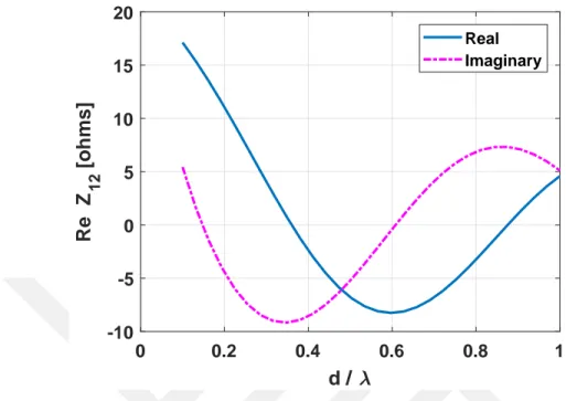
Figure 3.2: Real part of mutual impedance between two parallel dipole antennas as a function of spacing relative to wavelength with L = 0.4781λ and a = 0.001λ. Geometry shown in Fig. 3.1
Figure 3.3: Imaginary part of mutual impedance between two parallel dipole antennas as a function of spacing relative to wavelength with L = 0.4781λ and a = 0.001λ. Geometry shown in Fig. 3.1.
3.1.1.2 Staggered
Figure 3.4: Two identical parallel dipole antennas in staggered arrangement with length L = 0.4781λ, radius a = 0.001λ, fixed horizontal separation of 0.25λ, and staggered by h/λ.
The mutual impedance between two staggered dipole antennas, as a function of spacing relative to wavelength, which were computed by [2], were removed from the later editions of the book due to ambiguity in the results. The correct results for this case are presented below in Figs. 3.5 and 3.6.
0 0.5 1 1.5 2 h / λ -10 0 10 20 30 40 Re Z 1 2 [ohms]
Figure 3.5: Real part of mutual impedance between two identical but staggered dipole antennas of length L = 0.4781λ, radius a = 0.001λ, fixed horizontal separation of 0.25λ, and staggered by h/λ. 0 0.5 1 1.5 2 h / λ -40 -30 -20 -10 0 10 Im Z 1 2 [ohms]
It can be noted easily when h/λ = 0, the case is similar to that of non-staggered antenna and by examining the mutual impedance at d/λ = 0.25, the value of Fig. 3.2 matches with that of Fig. 3.5. Similarly, the same holds true for Fig. 3.3 and Fig. 3.6, which also verifies the authenticity of the results. These results were also verified with [13].
3.1.1.3 Collinear
Figure 3.7: Two dipole antennas in collinear arrangement as a function of spacing relative to wavelength with length L = 0.4781λ and radius a = 0.001λ.
Figure 3.8: Real part of mutual impedance between two collinear dipole antennas as a function of spacing relative to wavelength with length L = 0.4781λ and radius a = 0.001λ.
Figure 3.9: Imaginary part of mutual impedance between two collinear dipole antennas as a function of spacing relative to wavelength with length L = 0.4781λ and radius a = 0.001λ.
3.1.2 Mutual Coupling Compensation
The following subsections present results for the the mutual compensation technique that has been applied to different array configurations shown in the above sections. The un-compensated, un-compensated, and pattern multiplication patterns are compared. From these patterns it can be observed that the compensation technique explained in section 2.6 works effectively.
3.1.2.1 Two element Uniform Linear Array (ULA)
Figure 3.10: Two parallel antennas of length λ/2 with a = λ/200.
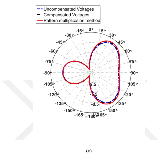
A two-element dipole antenna array similar to that of [15] with length λ/2 and radius λ/200 is used as shown in Fig. 3.10. The antennas are center fed with a magnetic frill source. The antenna element spacing is varied from 0.1λ to 0.5λ. The source internal impedance Z0 is 50 Ω and the original excitation voltage sources are Vg1= 1 V and Vg2 = 1∠135◦V . The
compensated voltages are tabulated in Table 3.1. The results are in close agreement with [15] and [14]. The resultant far field patterns in Figs. 3.11(a-e) show the far field patterns due to the uncompensated voltages, compensated voltages and pattern multiplication method in the plane perpendicular to the dipole axis. It can be observed that the array patterns due to the compensated voltages is almost the same as that of the isolated pattern results computed using pattern multiplication method. When the antennas are spaced closely, there is strong coupling between the antennas. This is evident from Fig. 3.24a as well as the compensated voltages in Table 3.1. The pattern due to the compensated voltage is in close approximation with that of the array factor pattern. As the distance between the dipoles increases the
mutual coupling decreases, therefore, at d = 0.5λ the compensated voltages in Table 3.1 become closer to the original voltages.
0° 15 ° 30° 45° 60° 75° 90° 105° 120° 135° 150° 165° ±180° -165° -150° -135° -120° -105° -90° -75° -60° -45° -30° -15° -15 -10 -5 0 Uncompensated Voltages Compensated Voltages Pattern multiplication method
(a) 0° 15° 30° 45° 60° 75° 90° 105° 120° 135° 150° 165° ±180° -165° -150° -135° -120° -105° -90° -75° -60° -45° -30° -15° -15 -10 -5 0 Uncompensated Voltages Compensated Voltages Pattern multiplication method
0° 15° 30° 45° 60° 75° 90° 105° 120° 135° 150° 165° ±180° -165° -150° -135° -120° -105° -90° -75° -60° -45° -30° -15° -15 -10 -5 0 Uncompensated Voltages Compensated Voltages Pattern multiplication method
(c) 0° 15° 30° 45° 60° 75° 90° 105° 120° 135° 150° 165° ±180° -165° -150° -135° -120° -105° -90° -75° -60° -45° -30° -15° -15 -10 -5 0 Uncompensated Voltages Compensated Voltages Pattern multiplication method
0° 15° 30° 45° 60° 75° 90° 105° 120° 135° 150° 165° ±180° -165° -150° -135° -120° -105° -90° -75° -60° -45° -30° -15° -15 -10 -5 0 Uncompensated Voltages Compensated Voltages Pattern multiplication method
(e)
Figure 3.11: Radiation patterns for two parallel dipole antennas with different element separa-tions. (a) d = 0.1λ (b) d = 0.2λ (c) d = 0.3λ (d) d = 0.4λ (e) d = 0.5λ.
Table 3.1: Compensation voltages Vs10 and Vs20 for the two element dipole array for different element separations. Antenna separation d(λ) Vs10 , (V ) Vs20 , (V ) 0.1 0.870∠31.58◦ 0.566∠104◦ 0.2 1.06∠23.7◦ 0.524∠134◦ 0.3 1.20∠15.3◦ 0.692∠151◦ 0.4 1.27∠6.81◦ 0.893∠153◦ 0.5 1.25∠ − 1.01◦ 1.05∠149◦
3.1.2.2 Five Element Uniform Linear Array
Figure 3.12: Five dipole antennas of length λ/2, a = λ/200 and spacing d.
A five element uniform linear array of dipoles as shown in Fig. 3.12 is studied in two different configurations similar to that in [15] and [14]. Same parameters for length, radius and internal source impedances are used as in the case of two-element dipole arrray except for excitation voltages and element spacing. In the first case, d = 0.5λ is used as element spacing and main-beam direction is excited at ϕ = 45◦. The excitation voltages are shown in Table 3.3 [15]. For the second case, d = 0.3λ and ϕ = 60◦. The resultant far field patterns in the plane perpendicular to the dipole axis are shown in Figs. 3.13 and 3.14. The compensated voltages for both cases are tabulated in Table 3.2 which are in close agreement with [15] and [14].
0° 15 ° 30° 45° 60° 75° 90° 105° 120° 135° 150° 165° ±180° -165° -150° -135° -120° -105° -90° -75° -60° -45° -30° -15° -15 -10 -5 0 Uncompensated Voltages Compensated Voltages Pattern multiplication method
Figure 3.13: Radiation pattern for five-element dipole array with separation d = 0.5λ and main-beam direction ϕ = 45◦.
Table 3.2: Compensation voltages for the five-element dipole array with different inter-element separations d and main-beam directions ϕ.
Voltages ϕ = 45◦, d = 0.5λ ϕ = 60◦, d = 0.3λ Vs10 0.803∠19◦ 0.770∠ − 5.34◦ Vs20 1.12∠ − 113◦ 1.19∠ − 71.96◦ Vs30 1.30∠110◦ 1.29∠ − 127◦ Vs40 1.37∠ − 26.8◦ 1.29∠159◦ Vs50 1.28∠ − 168◦ 1.25∠116◦
0° 15 ° 30° 45° 60° 75° 90° 105° 120° 135° 150° 165° ±180° -165° -150° -135° -120° -105° -90° -75° -60° -45° -30° -15° -15 -10 -5 0 Uncompensated Voltages Compensated Voltages Pattern multiplication method
Figure 3.14: Radiation pattern for five-element dipole array with separation d = 0.3λ and main-beam direction ϕ = 60◦.
Table 3.3: Excitation voltages for the five-element dipole array with different inter-element sepa-rations d and main-beam directions ϕ.
Voltages ϕ = 45◦, d = 0.5λ ϕ = 60◦, d = 0.3λ Vs1 1∠0◦ 1∠0◦ Vs2 1∠ − 127.28◦ 1∠ − 54◦ Vs3 1∠ − 254.56◦ 1∠ − 108◦ Vs4 1∠ − 381.84◦ 1∠ − 162◦ Vs5 1∠ − 509.12◦ 1∠ − 216◦
The results infer that when d = 0.3λ, there is strong mutual coupling which is evident from Table. 3.2 and its corresponding excitation voltages.
3.2
Non-Identical Arrays
3.2.1 Mutual Impedance
The mutual impedance for two element non-identical arrays is calculated in this section. Similar to Section 3.1, three different configurations are studied. Two dipoles of unequal lengths are considered such that L1 = λ/2 and L2 = λ/3. The radius a for both the wires is
same, a = 0.001λ. The mutual impedance of unequal length dipoles for infinitely thin wires has been studied in [13]. It should be noted that in [13], the author considers infinitely thin wires where as in this thesis a finite wire radius is considered hence the mutual impedances presented in [13] and here are not exactly the same but in close approximation in the overall trend. Figure 3.15 to Fig. 3.20 show the geometry of the arrays considered and the computed mutual impedances.
3.2.1.1 Non Staggered Array
Figure 3.15: Two parallel dipole antennas in non-staggered arrangement of lengths λ/2 and λ/3 as a function of spacing relative to wavelength with radius a = 0.001λ.
0 0.2 0.4 0.6 0.8 1 d / -20 -10 0 10 20 30 40 Re Z 1 2 [ohms] Real Imaginary
Figure 3.16: Mutual impedance curves between two parallel antennas in non-staggered arrange-ment of lengths λ/2 and λ/3 as a function of spacing relative to wavelength with a = 0.001λ.
3.2.1.2 Staggered Array
Figure 3.17: Two parallel dipole antennas of lengths λ/2 and λ/3 in staggered arrangement as a function of spacing relative to wavelength with a = 0.001λ, horizontal separation d and staggered by h = λ/4.
0 0.2 0.4 0.6 0.8 1 d / -10 -5 0 5 10 15 20 Re Z 1 2 [ohms] Real Imaginary
Figure 3.18: Mutual impedance curves between two parallel antennas of lengths λ/2 and λ/3 with a = 0.001λ, staggered by h = λ/4.
0 0.2 0.4 0.6 0.8 1 d / -5 0 5 10 15 20 25 30 Re Z 1 2 [ohms] Real Imaginary
Figure 3.20: Mutual impedance curves for two dipole antennas of lengths λ/2 and λ/3 in a collinear arrangement with radius a = 0.001λ.
3.2.2 Mutual Coupling Compensation
3.2.2.1 Two element Non-Staggered Array
The compensation for two element non-identical array as shown in Fig. 3.21 is computed in this section. The dipoles are excited with a magnetic frill source at their center. The original excitation voltage sources are Vg1 = 1 V and Vg2 = 1∠135◦V , respectively. The antenna
element spacing is varied from 0.1λ to 0.5λ. The compensated voltages are tabulated in Table 3.4. The resultant far field patterns in Figs. 3.22(a-e) show the far field patterns due to the uncompensated voltages, compensated voltages and pattern multiplication method in the plane perpendicular to the dipole axis, i.e., the H-plane. As compared to the identical two element dipole case in Fig. 3.11 and Table 3.1, it can be noted that the mutual coupling is weaker here since L2 is shorter than L1 we expect less coupling.
Figure 3.21: Two parallel antennas in non-staggered arrangement of lengths λ/2 and λ/3 as a function of spacing relative to wavelength with radius a = 0.001λ, and separation d.
Table 3.4: Compensation voltages Vs10 and Vs20 of two-element non-identical non-staggered dipole array for different antenna separations.
Antenna separation d(λ) Vs10 , (V ) Vs20 , (V ) 0.1 0.8199∠−6.46◦ 0.7517∠128.0◦ 0.2 0.8307∠−0.65◦ 0.7723∠135.2◦ 0.3 0.8752∠3.56◦ 0.8314∠140.7◦ 0.4 0.9360∠5.29◦ 0.9117∠142.9◦ 0.5 0.9921∠4.92◦ 0.9877∠142.3◦
0° 15° 30° 45° 60° 75° 90° 105° 120° 135° 150° 165° ±180° -165° -150° -135° -120° -105° -90° -75° -60° -45° -30° -15° -4 -3 -2 -1 0 Uncompensated Voltages Compensated Voltages Pattern multiplication method
(a) 0° 15° 30° 45° 60° 75° 90° 105° 120° 135° 150° 165° ±180° -165° -150° -135° -120° -105° -90° -75° -60° -45° -30° -15° -4 -3 -2 -1 0 Uncompensated Voltages Compensated Voltages Pattern multiplication method
0° 15° 30° 45° 60° 75° 90° 105° 120° 135° 150° 165° ±180° -165° -150° -135° -120° -105° -90° -75° -60° -45° -30° -15° -4 -3 -2 -1 0 Uncompensated Voltages Compensated Voltages Pattern multiplication method
(c) 0° 15° 30° 45° 60° 75° 90° 105° 120° 135° 150° 165° ±180° -165° -150° -135° -120° -105° -90° -75° -60° -45° -30° -15° -4 -3 -2 -1 0 Uncompensated Voltages Compensated Voltages Pattern multiplication method
(e)
Figure 3.22: Radiation pattern of two-elements non-identical non-staggered dipoles with different element separations. (a) d = 0.1λ (b) d = 0.2λ (c) d = 0.3λ (d) d = 0.4λ (e) d = 0.5λ.
3.2.2.2 Two Elements Staggered Array
The compensation for two elements non-identical staggered array as shown in Fig. 3.23 is computed in this section. The dipoles are staggered by h = λ/4. With excitation source voltages Vg1 = 1 V and Vg2 = 1∠135◦V and element spacing varied from 0.1λ to 0.5λ,
the compensated voltages are tabulated in Table 3.5. The resultant far field patterns in Figs. 3.24(a-e) show the far field patterns due to the uncompensated voltages, compensated voltages and pattern multiplication method in the plane perpendicular to the dipole axis. As compared to the identical two element dipole case in Fig. 3.11 and Table 3.1, it can be noted that the mutual coupling is weaker here since L2 is not in line with L1, which results
Figure 3.23: Two parallel dipole antennas of lengths λ/2 and λ/3 in staggered arrangement as a function of spacing relative to wavelength with radius a = 0.001λ, and staggered by h = λ/4.
Table 3.5: Compensation voltages Vs10 and Vs20 for two-elements non-identical staggered dipole array for different antenna separations.
Antenna separation d(λ) Vs10 , (V ) Vs20 , (V ) 0.1 0.9278∠−4.83◦ 0.8893∠129.1◦ 0.2 0.9230∠−0.81◦ 0.8902∠134.5◦ 0.3 0.9453∠1.71◦ 0.9221∠137.9◦ 0.4 0.9782∠2.62◦ 0.9670∠139.1◦ 0.5 1.0081∠2.27◦ 1.0082∠138.5◦