See discussions, stats, and author profiles for this publication at: https://www.researchgate.net/publication/281116301
Strain modulated band gaps of semiconducting zigzag single walled carbon
nanotubes
Article in Journal of Optoelectronics and Advanced Materials · August 2015
CITATIONS 2 READS 108 3 authors, including: Gulay Dereli Koc University 19PUBLICATIONS 325CITATIONS SEE PROFILE Önder Eyecioğlu Gelisim Üniversitesi 7PUBLICATIONS 19CITATIONS SEE PROFILE
All content following this page was uploaded by Önder Eyecioğlu on 21 August 2015.
Strain modulated band gaps of semiconducting zigzag
single walled carbon nanotubes
G. DERELIa , Ö. EYECIOĞLUb* , B. S. MISIRLIOĞLUc
aKoc University, Apt.18/4, Istanbul, 34450, Turkey b
Istanbul Gelisim University, Department of Mechatronics Engineering, Istanbul, 34310,Turkey
cYildiz Technical University, Department of Physics, Istanbul, 34220, Turkey
Strain can alter the electronic properties of materials. At the nanoscale, small displacements of atoms could have large effects. In this study, we have examined how elastic strain can modify the energy band gaps of semiconducting zigzag Single Walled Carbon Nanotubes (SWCNTs). The electronic structure of SWCNTs have been computed for each deformed configurations by means of real space, Order(N) Tight Binding Molecular Dynamic (O(N) TBMD) simulations. During the applications of uniaxial strain, carbon atoms are moved slightly from their equilibrium positions, but their atomic bonds are not broken. Three different kinds of semiconducting zigzag SWCNTs are chosen. (12,0) SWCNT, although a semiconducting SWCNT, is quasi-metallic in its pristine state. Application of stretching and compression opens its band gap. Thus under strain (12,0) SWCNT shows metallic-semiconducting transitions. (13,0) and (14,0) zigzag SWCNTs are semiconductors having energy band gap values of 0.44eV and 0.55eV in their pristine state. The energy band gap of (13,0) SWCNT decreases with increasing absolute value of compression. On the other hand, the energy band gap of (14,0) SWCNT decreases with increasing value of tension. So in both cases, the energy band gap closes and semiconducting - metallic transitions are observed. Flexibilities of the stretched hexagonal network of SWCNTs are displayed in terms of carbon-carbon bond-lengths, bond-angles and radial distribution functions. Correlations between the strain induced structural changes and the electronic properties of SWCNTs are discussed.
(Received April 9, 2015; accepted June 24, 2015)
Keywords: Single-Wall Carbon Nanotubes, Tight-binding Molecular Dynamics, Order N, Strain, Energy Band Gaps
1. Introduction
Graphene and SWCNTs actually have very similar structures. The difference is that graphene is a flat layer of carbon atoms, only one atom thick, whereas SWCNTs are sheets of carbon atoms rolled up into a tube shape. Graphene, despite its promising charge transport properties, due to the lack of an intrinsic bandgap faces problems to function as a switch in transistor devices. Zero band gap nature of the graphene is an unfavorable property and application of strain works in favor for graphene. Thus strain induced band gap engineering improves the electronic properties of graphene. On the other hand, SWCNTs can sustain their stability up to very high temperatures [1] and defect free SWCNTs can be stretched in axial direction 130% of the relaxed tube length without any bond breaking or 5-7 defects formation [2,3]. Application of strain can open or close the energy band gap depending on the type of SWCNT (armchair or zigzag). SWCNT’s electronic properties mainly depend on the helical arrangement of atoms [4]. The structure of a SWCNT is described by the chiral vector
2 1 ma
a n Ch where n and m are integers and a1and a2 are the unit vectors of graphene lattice. Depending on the chiral vector, SWCNTs can be classified into three types, namely, armchair (n,n),zigzag (n,0) and chiral (n,m). Achiral SWCNTs of the armchair (n,n) types are always metallic, and the zigzag (n,0) SWCNTs are only metallic when n is a multiple of 3. Application of uniaxial strain
(tensile or compressive) will not cause a metal-insulator transition for the armchair (n,n) SWCNTs. However, it can open up an energy band gap for the zigzag (n,0) when n is a multiple of 3. When n is not a multiple of 3, n (mod 3) can be either 1 or 2. These types of zigzag (n,0) SWCNTs are moderate-band gap semiconductors but their band gaps react differently to tensile stretching and compressing. Band gaps of n (mod 3) = 1 SWCNTs close with compressive strain and open up with tensile strain. On the other hand, in the case of n (mod 3) = 2, a SWCNT’s band gap decreases for tensile strain and opens up for compressive strain. The electronic band structure of SWCNT is derived from the graphene analogy. The Brillouin zone of graphene is a hexagon. The valence bands touch the conduction bands at the corners of the hexagon giving the semi-metallic characteristic of graphene. A SWCNT is a rolled-up graphene sheet and the periodic boundary conditions quantize the components of the electronic wave vectors along the circumferential direction. When the quantized components of the electronic wave vectors along the circumferential direction intersect the graphene Fermi sur- face, SWCNTs show metallic characteristics, otherwise not. For example (n,0) zigzag SWCNTs are metallic when n (mod 3) = 0, because only in this case quantized k vectors cross the vertices of the hexagonal Brillouin zone of the graphene. On the other hand n (mod 3) = 1 or 2 types of (n, 0) zigzag SWCNTs are semiconductors with no allowed electronic wave vectors crossing the vertices of the graphene’s Brillouin
Strain modulated band gaps of semiconducting zigzag single walled carbon nanotubes 919 zone. Tight-binding [5,6,7], ab initio GGA, LDA
computations [8,9] and first principle DFT studies [10,11,12] have shown that tensile deformations will modify the band gap of the carbon nanotubes. The application of the conventional ab initio electronic structure calculations to large systems is impeded by their inherent O(N3) scaling properties with N the number of atoms. In order to overcome this difficulty, efficient linear scaling algorithms, which are referred to as O(N) methods, have been developed. Real space algorithms have been successfully used to perform ab initio electronic structure calculations [13,14,15,16]. The main objective of this paper is to make use of real space O(N) parallel tight-binding molecular-dynamics algorithms [17,18,19] one of us (G. Dereli) has developed in studying the electronic structure of strained SWCNTs with diameters going up to 1 nm. It is of interest to investigate, Whether a
semiconducting zigzag SWCNT still remain
semiconducting after stretching and compressing? We applied the real space O(N) and parallelization techniques in particular to (12,0), (13,0) and (14,0) zigzag SWCNTs according to n (mod 3) = 0, n (mod 3) = 1 and n (mod 3) = 2 classification. Dimensions of the selected zigzag SWCNTs are given in Table 1. Electronic temperature is set to 300K. It is found that tubes sustain their tensile stability under applied strain values and the total energy quadratically increases under both tension and compression. We displayed the address of the strain that causes the first metal semiconductor and semiconductor - metal transitions in the zigzag SWCNTs. Zigzag SWCNTs that are represented as n (mod 3) = 0 are metallic and all others (i.e. n (mod 3) = 1 and n (mod 3) = 2) are semiconducting in unstrained conditions.
The energy band gap of zigzag (12,0) SWCNT with chiral vectors n (mod 3) = 0 increases so metallic-semiconducting transitions occur under both tension and compression. On the other hand, the energy band gap of zigzag (13,0) SWCNT with chiral vectors n (mod 3) = 1 increases under tension. However, it decreases under compression so semiconducting - metallic transition occurs. The energy band gap of zigzag (14,0) SWCNT with chiral vectors n (mod 3) = 2 increases under compression. However, it decreases under tension so semiconducting - metallic transition occurs. Our real space O(N) TBMD results support the trends of previous first principle studies of [8,9,10,11] and k-space tight-binding band gap calculations of [7] and reveals significant information of electronic behaviors of strained zigzag SWCNTs in real space. Since samples used in most of the experiments are mixtures of different chiral indices, a direct comparison with theoretical calculation is not possible. Real space results of the O(N) TBMD algorithms offer an alternative technique besides ab initio simulations and the model potential ones. Results are also substantiated by the changes observed in the radial distribution, bond- length distribution and bond-angle distribution functions in the paper.
2. Method
We use the parallel O(N) TBMD simulation technique which is successfully applied to the SWCNTs by G. Dereli et al. [17,18,19] in order to study the energetics and electronic properties of (12,0), (13,0) and (14,0) SWCNTs (Table 1).
Table 1. Physical properties of SWCNTs for tensile Simulations 𝑛(mod 3) = 0 (12,0) 𝑛(mod 3) = 1 (13,0) 𝑛(mod 3) = 2 (14,0) Buffer Skin Size (Å) 4.5 4.6 4.5 Number of Atoms 240 260 280 Radius (𝑛𝑚) 0.47 0.51 0.55 Length (𝑛𝑚) 1.99 1.99 1.99
Simulations are performed in two steps. Firstly, SWCNTs are simulated until their structural stability is sustained (3000 MD steps of simulation time is used and each time step is chosen as 1fs). A longer number of MD steps was tested (10000 MD steps) and it was seen that energy fluctuations remain unchanged. Secondly, axial strain is applied along the SWCNT axis and the tube is equilibrated for another 2000 MD steps. At each MD step, total energy and atomic forces are calculated. For MD scheme, equations of motion are integrated by using Velocity Verlet algorithm. Periodic boundary condition is applied in the uniaxial direction. All the simulations presented here are carried out in the canonical (NVT) ensemble. The results for sequential and parallel runs are compared and assured that they are the same both in numerical accuracy and in physical aspects.
In the classical TBMD, electronic structure of the system can be calculated by the TBMD Hamiltonian so that the quantum mechanical many-body nature is taken into account [20, 21]
n rep n n TBMD f T U m P H ( , ) 2 2 (1)The forces needed to move atoms is evaluated from TBMD Hamiltonian as r U T f r H f n n rep n n tot
( , ) , (2)the second term on the right hand side of the Eq. (2) is a repulsive force that will be given analytically as a function of the interatomic distance [22]. On the other hand the first term on the RHS of Eq. (2) is the Hellmann-Feynman contribution to the total force
n l n l l l l n l n n n n n C r r H C T T f r H
( , ) 2 ( , ) ( ) (3)Total energy, Etot, of a system of ion cores and
valance electrons can be written as:
n rep bs ee ii n TOT f T U U E E E ( , ) (4)where f (εn,T ) is the Fermi-Dirac distribution function.
The sum of all the single particle energies is commonly called the band structure energy Ebs. In order to calculate
the band structure energy and Hellman Feynman forces, we need the full spectrum of eigenvalues εn determined by
solving the secular Eq. (5) and the corresponding eigenvectors n l C: ( ) 0
n l l l n l l C H l (5)We diagonalize the TBMD Hamiltonian matrix at every time step of the simulation. Standard diagonalization of the TB matrix requires a computation time in cubic scaling with respect to the number of atoms and dominates the overall computational workload of the TBMD simulations. On the other hand, O(N) methods solve the band energy in real space and make the approximation that only the local environment contributes to the bonding and hence the band energy of each atom. In this case, the computation time would be in linear scaling with respect to the number of atoms [23]. One of the O (N) methods used to carry out quantum calculation is the divide and conquer (DAC) approach [24, 25]. The key idea of this approach is to provide a description of a large system in terms of contributions from subsystems. The system is split into subsystems described by a set of basis set of neigh- boring atoms that are called buffer. Each subsystem is solved separately, and the total electron density and the energy of the system are obtained by summing the corresponding contribution from all subsystems [18]. The accuracy of this description depends on the buffer size. The results obtained with the O(N) algorithm must be consistent with O(N3) results for the same system. Buffer skin size is calculated as 4.5 Å for (12,0) and (14,0) SWCNTs and 4.6 Å for (13,0) SWCNT [26]. Moreover, O(N) technique can be efficiently parallelized by use of message passing interface such as PVM. Details of the technique can be followed in [17, 18, 19].
Uniaxial strain is applied to the SWCNTs along the axial (z) direction and allowed to relax along radial direction. So the volume of the tube is kept constant. The axial strain is obtained from ε = (l − l0)/l0 where l0 is the
equilibrium length in the axial direction for unstrained SWCNT and l is the corresponding length in the strained SWCNT. Positive strain values correspond to tension and negative strain values to compression. We have calculated the total energy and energy band gap of (12,0), (13,0) and (14,0) zigzag SWCNTs under axial tension and compression. The energy band gap of the strained SWCNTs is determined from real space electronic density of states (eDOS) which is obtained from the general formula ( ) ( ) ( ) ) ( N N d dN g (6)
where N is number of electrons in the system and equals to
2 4 1 4 1 ) , ( * / ) (( 1 2 ) (
NCELL N i N j b i i j H T k E f E N (7)The existence of populated electronic states near Fermi energy level on the eDOS (Eq. (6)) determines the energy band gap. Simulations are performed at room temperature (300K) and the periodic boundary condition (PBC) is applied along the z direction.
3. Results and discussion
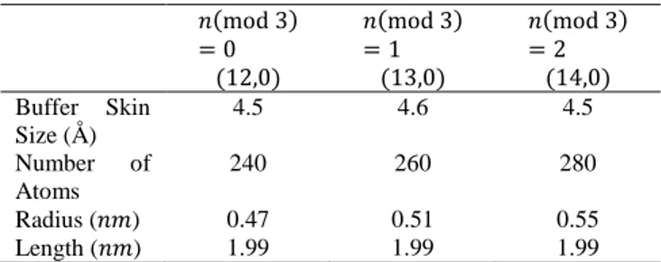
In this study, we have examined how elastic strain can alter the band gap of semiconducting zigzag SWCNTs. Figure.1 summarizes the effect of positive and negative strains applied to semiconducting zigzag (12,0), (13,0) and (14, 0) SWCNTs. First 3000 MD steps of simulations show the total energy fluctuations of the pristine SWCNTs (without strain). Longer simulation times have been tested but the energy fluctuations remained the same.
Fig. 1: Variation of the total energy (eV /Atom) as a function of applied strain. First 3000 MD steps give the energy of pristine SWCNTs (without strain), next 2000 MD steps give the energy under the applied strain. Positive and negative strain values correspond to the tension and compression, respectively. Simulations are
performed at 300K.
Several strain values are applied to a pristine tube to study the strain rate. Strain is obtained from ε = (l − l0)/l0 ,
Strain modulated band gaps of semiconducting zigzag single walled carbon nanotubes 921 strain, respectively. Positive strain values correspond to
tension and the negative strain values to compression. Strain is applied in steps of 1% in the elastic range of (−8%) to (+8%). SWCNTs are equilibrated under strain for another 2000 MD steps. Short fluctuations in total energy values indicate that (12,0), (13,0) and (14,0) zigzag SWCNTs are stable under applied strain values. Total energy values that are calculated from Figure 1 and presented as functions of strain in Figure 2.
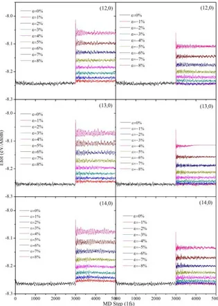
Fig. 2: Total energy (eV /Atom) versus strain curves of (a) (12, 0) SWCNT, (b) (13, 0) SWCNT and (c) (14, 0) SWCNT. The insets show the variation of band structure (Ebs) and repulsive (Erep) energies with
respect to the applied strain.
Total energy increases quadratically with the application of positive and negative strains, indicating the elastic behavior of the SWCNTs. At zero strain, minimum values of the total energy read as −8.24 (eV /Atom), −8.26 (eV /Atom) and −8.27 (eV /Atom) for zigzag (12, 0), (13, 0) and (14, 0) SWCNTs, respectively. Insets of Figure 2 show the band structure Ebs and the repulsive energy Erep
contributions to total energy.
Next, we investigated the strain induced change of electronic density of states (eDOS) of individual nanotubes. eDOS of zigzag (12,0), (13,0) and (14,0) SWCNTs are calculated from Eq. (6) and plotted in Figures 3, 4 and 5, respectively. eDOS graphs are normalized by moving the Fermi energy level to zero on the x axis. The existence of electronic states near Fermi energy level through the eDOS graphs defines the energy band gap (Eg) of SWCNTs. Figs. (3 a,b,c) display the
eDOS of (12,0) SWCNT under the strain values of 0, +8%, −8%, respectively. Here, a positive strain value corresponds to axial tension and a negative strain value corresponds to axial compression. In Fig. 3 a, (12, 0) SWCNT has no band gap at zero strain, indicating metallic behavior of the tube in the pristine state. When tensile strain is applied, a band gap appears and it opens up under both tension and compression as depicted in Figures 3 b and c. (12,0) SWCNT which is quasi metallic in the pristine state, with the application of positive and negative
strains can undergo band gap increases, leading to a metallic-semiconducting transition of (12, 0) tube. Fig. (4 a,b,c) give the change in the eDOS of (13, 0) SWCNT under the strain values of 0, +6%, −6%, respectively. In Fig. 4a, it is shown that the (13, 0) tube has a band gap at the strain of 0 and the gap disappears at the strain of −6% (Fig. 4c). This indicates that the tube, which is semiconducting in pristine state becomes metallic as the compression is applied. On the other hand, Figure 4b shows that at the strain of +6%, the band gap increases which means that (13, 0) tube retains its semiconducting behavior during tension. Figures (5 a, b, c) show the eDOS behavior of (14,0) SWCNT under the strain values of 0, +5%, −5%, respectively. In Figure 5a, it is shown that (14,0) tube has a band gap at zero strain similar to (13,0) SWCNT. However, in contrast with the (13,0) tube, at the strain of +5% the band gap disappears and the gap opens at the strain of −5%. So it is shown that (14,0) SWCNT shows semiconducting-metallic transition during tension. It retains its semiconducting behavior during compression.
Fig. 3: Calculated eDOS structure of (12, 0) SWCNT at different uniaxial strain: (a) ε = 0% (pristine state), (b) ε = +8% (tension) and (c)ε = −8% (compression).
Fig. 4: Calculated eDOS structure of (13, 0) SWCNT at different uniaxial strain: (a) ε = 0% (pristine state), (b) ε = +6% (tension) and (c) ε = −6% (compression).
Fig. 5. Calculated eDOS structure of (14, 0) SWCNT at different uniaxial strain: (a)ε = 0% (pristine state), (b) ε = +5% (tension) and (c)ε = −5% (compression).
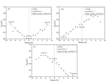
Next, we investigated the strain-induced change of band structure of individual nanotubes. The energy band gaps of (12,0), (13,0) and (14,0) zigzag SWCNTs are obtained from the existence of electronic states near Fermi energy level on the eDOS graphs and they are given as a function of strain in Fig. 6 a, b, c, respectively. As shown in Figure 6a, the band gap of (12, 0) nanotube is 0.01eV at zero strain. When tensile strain is applied, a band gap appears and increases up to 0.47eV under both +8% tension and −8% compression. These results are consistent with the first principle results of [10]. Fig. 6b shows that the band gap of (13, 0) nanotube is 0.44eV at zero strain. When tensile compression is applied, the band gap decreases and reaches 0.11eV under −8% tensile strain. On the other hand, the band gap of (13,0) nanotube increases with increasing tensile tension and reaches 0.74eV for +6% tensile strain. Our results are consistent with the first principle results of [8, 9, 10, 11, 12] and tight binding calculations of [7] for similar chirality SWCNTs. Figure 6c shows that the band gap of (14, 0) nanotube is 0.55eV at zero strain. When tensile tension is applied, the band gap decreases and reaches 0.04eV under +6% tensile strain. On the other hand, the band gap of (14,0) nanotube increases with increasing value of compression and reaches 0.67eV for −5% tensile strain. Our results are consistent with the first principle results of [10] and k-space tight binding calculations of [7] for similar chirality SWCNTs.
Fig. 6. Calculated energy band gap (eV ) versus uniaxial strain curves of (a) (12, 0) SWCNT, (b) (13, 0) SWCNT
and (c) (14, 0) SWCNT.
Fig. 7. Calculated energy band gap (eV ) modifications of (12, 0), (13, 0) and (14, 0) SWCNTs as a function of
uniaxial strain.
Fig. 8. Radial distribution functions of simulated (a) (12, 0) SWCNT, (b) (13, 0)SWCNT and (c) (14, 0)
Strain modulated band gaps of semiconducting zigzag single walled carbon nanotubes 923 Fig. 7 summarizes the strain-induced band gap
changes of (12,0), (13,0) and (14,0) SWCNTs. Previous theoretical predictions are confirmed by studying small axial strains in broad range. Small axial strains such as 0.1% can induce band gap increases or decreases in SWCNTs. For high strain rates, the changes in the Radial Distribution Function (RDF), Bond Length Distribution Function (BLDF) and Bond Angle Distribution Function (BADF) are given through Figures 8, 9 and 10. In the graphs, two-thirds of the bond lengths and one-third of the bond angles increase (decrease) when the tube is elongated (contracted) as expected. Bond angles and bond lengths are the two important factors that control the deformation. The effect of strain on the bonds is such that it alters the angles between two neighboring carbon bonds and changes the lengths of the C − C bonds.
Fig. 9. Bond-length distribution functions of simulated (a) (12, 0) SWCNT, (b) (13, 0)SWCNT and (c) (14, 0)
SWCNT.
Fig. 10: Bond-angle distribution functions of simulated (a) (12, 0) SWCNT, (b) (13, 0)SWCNT and (c) (14, 0)
SWCNT.
RDF graphs of unstrained SWCNTs, display a first peak at the nearest neighbor (nn) distance of 1.41 Å, second peak is at the second nn distance of 2.43 Å and the third peak is at 2.85 Å. For simulated pristine SWCNTs, Bond Angle Distribution Function (BADF) peaks around 119.4 degree and Bond Length Distribution Function (BLDF) around 1.42 Å.
Table 2: Radial Distribution Function (RDF), Bond Length Distribution Function (BLDF) and Bond Angle Distribution Function (BADF) peak positions at zero strain and also in strained conditions.
Physical Property BLDF (Å) BADF (deg ) RDF (Å) Strain(%) −6% 0% +6% −6% 0% +6% −6% 0% +6% (12, 0) 1.40 1.42 1.46 115.8 119.4 123 2.36 2.43 2.39 (13, 0) 1.41 1.42 1.44 115.8 119.4 123 2.38 2.43 2.39 (14, 0) 1.41 1.42 1.45 117 119.4 126.6 2.38 2.44 2.27
Numerical values of changes with elongation (contraction) are given in Table 2. Results are substantiated by the changes observed in the radial distribution, bond-length distribution and bond-angle distribution functions.
4. Conclusions
In this paper, we tried to find an answer to the question: “Whether a semiconducting zigzag Single-
Walled Carbon Nanotube (SWCNT) still remain semiconducting after stretching and compressing?”
We have used Order (N) TBMD algorithms which are successfully applied in real space simulations of (SWCNTs) [1, 2, 3, 17, 18, 19]. In the study, we used zigzag (n, 0) SWCNTs. These SWCNTs are only quasi metallic when n is a multiple of 3, otherwise they are semiconducting. In particular, (12,0), (13,0) and (14,0) zigzag SWCNTs are chosen according to n (mod 3) = 0, n (mod 3) = 1 and n (mod 3) = 2 classification. Nevertheless, uniaxial deformations are found to dissimilarly affect the band structures of such SWCNTs.
(13,0) SWCNT representing n (mod 3) = 1 type of SWCNT with 0.44eV energy band gap grows up to a maximum value of 0.74eV when the strain parameter achieves a value of 6%. On the other hand, (14,0) SWCNT representing n (mod 3) = 2 type of SWCNT with 0.50eV energy band gap reduces to 0.04eV at the strain parameter of 8%. Thus a semiconducting SWCNT no longer remains a semiconductor. On the other hand with the application of negative strain ( i.e compression) we observe the opposite behavior. Negative strain closes the band gap of (13,0) SWCNT. Semiconducting (13,0) SWCNT becomes metallic in conductivity. Application of negative strain in semiconducting (14,0) causes the evolution of the gap opening from 0.50eV to 0.67eV. The energy band gap of (12, 0) zigzag SWCNT with the chiral vector of n (mod 3) = 0 increases so that metallic- semiconducting transitions occur under both tension and compression.
It has been shown that armchair graphene ribbons having an edge with an armchair form, alternate periodically with width between metallic and semi- conducting behaviors, quite analogous to the behavior observed in SWCNTs [27]. Armchair graphene ribbons when rolled up into tube shape result in zigzag SWCNT. In this study, we used volume constant NVT algorithms; strain is applied along the z direction and SWCNT is allowed to relax along the radial direction in order to preserve the volume of the system. This process corresponds to width changes in armchair graphene ribbons.
This study provides useful insights for understanding the electronic behavior of deformed zigzag SWCNTs under uniaxial strain. The advantage of our technique is that the calculations are done in real space. Moreover, this study shows that O(N) TBMD simulation method is an efficient tool for clarifying the tensile behavior and electronic structure of SWCNTs which are important for designing the future SWCNT based electronic and opto electronic devices.
Acknowledgement
The research reported here is supported through the Yildiz Technical University Research Fund Project No: 2009-01-01-KAP01. Simulations are performed at the Carbon Nanotubes Simulation Laboratory at the Depart-
ment of Physics, Yildiz Technical University,
Istanbul,Turkey.(http://www.yildiz/edu/tr/˜gdereli/lab_ho mepage/index.html).
References
[1] G. Dereli, B. Süngü, C. Özdoğan, Nanotechnology 18, 245704 (2007).
[2] G. Dereli, B. Süngü, Phys. Rev. B 75, 184104 (2007). [3] G. Dereli, B. S. Misirlioglu, Ö.Eyecioğlu, N. Vardar, Comput. Mater. Sci. 69, 234 (2013).
[4] R. Saito, G.Dresselhaus, M. Dresselhaus, Physical Properties of Carbon Nanotubes, London: Imperial College Press (1998).
[5] G.Shan, S.Bao, Physica E 35, 161 (2006). [6] S.Ogata, Y.Shibutani, Phys. Rev. B 68, 165409 (2003).
[7] Y. Umeno, T. Kitamurai, Comput. Mater. Sci. 31, 33 (2004).
[8] T. Ito, K. Nishidate, M. Baba, M.Hasegawa, Surface Science 514, 222 (2002).
[9] A. Pullen, G. L. Zhao, D. Bagayoko, L. Yang, Phys. Rev. B 71, 205410 (2005).
[10] S. Sreekala, X.-H. Peng, P. M. Ajayan, S. K. Nayak, Phys. Rev. B 77, 155434 (2008).
[11] P. K. Valavala, D. Banyai, M. Seel, R. Pati, Phys. Rev. B 78, 235430 (2008).
[12] J.-M. Zhang, Rui-LiLiang, Ke-WeiXu, Physica B 405, 1329 (2010).
[13] M. B. Nardelli, Phys. Rev. B 60, 7828 (1999). [14] J.-L. Fattebert, J. Bernholc, Phys. Rev. B 62, 1713 (2000).
[15] L. Liu, C. S. Jayanthi, M. Tang, S. Y. Wu, T. W. Tombler, C.Zhou, L. Alexseyev, J. Kong, H. Dai, Phys. Rev. Lett. 84, 4950 (2000).
[16] T. Ozaki, K. Terakura, Phys. Rev. B 64 195126 (2001).
[17] C. Özdoğan, G. Dereli, T. Çağın, Comp. Phys. Commun. 148, 188 (2002).
[18] G. Dereli, C. Özdoğan, Phys. Rev. B 67, 035415 (2003).
[19] G. Dereli, C. Özdoğan, Phys. Rev. B 67, 035416 (2003).
[20] L. Colombo, Annual Reviews of Computational Physics 4, 147 (1996).
[21] L. Colombo, Comput. Mater. Sci. 12, 278 (1998). [22] C. H. Xu, C. Z. Wang, C. T. Chan, K. M. Ho, J. Phys.: Condens.Matter. 4, 6047 (1992). [23] P. Ordejon, Comput. Mater. Sci. 12, 157 (1998). [24] W. Yang, Phys. Rev. Lett. 66, 1438 (1991). [25] T. Zhu, W. Pan, W.Yang, Phys. Rev. B 53, 12713 (1996).
[26] Ö. Eyecioğlu, Computer simulations of electronic structure of carbon nanotubes, Ph.D. thesis, Yildiz Technical University, Istanbul, Turkey (2012). [27] K. Nakada, M. Fujita, G. Dresselhaus,
M. S. Dresselhaus, Phys Rev B Condens. Matter. 54, 17954 (1996).
____________________________
*
Corresponding author: [email protected]
View publication stats View publication stats