IEEE TRANSACTIONS ON ELECTRON DEVICES, VOL. 36. NO. 6, JUNE 1989 1009
Quantum Mechanical Simulation of Charge Transport
in
Very
Small Semiconductor Structures
M. C. YALABIK, G. NEOFOTISTOS, KARIM DIFF, HONG GUO, AND
JAMES D. GUNTON, MEMBER, IEEE
Abstract-A quantum mechanical simulation method of charge transport in very small semiconductor devices, based on the numerical solution of the time-dependent Schrodinger equation (coupled self-con- sistently to the Poisson equation to determine the electrostatic potential in the device), is presented. Carrier transport is considered within the effective mass approximation, while the effects of the electron-phonon interaction are included in an approximation that is consistent with the results of the perturbation theory and gives the correct two-point time correlation function. Numerical results for the transient behavior of a planar ultrasubmicrometer three-dimensional GaAs MESFET (gate length of 26 nm) are also presented. They indicate that extremely fast gate-step response times (switching times) characterize such short- channel GaAs devices.
I. INTRODUCTION
IMULATION of charge transport in very small geo-
S
metries has important applications in the field of semi-conductor devices, where the prediction and analysis of device operations can be carried out more economically through the use of computers. Several techniques have been used for the simulations, depending on the way the physics of the charge transport is modeled. If the mean free path of the carriers is much smaller than the typical geometric features of the structure, the diffusion equation may be used to describe the dynamics of the charges un- der the influence of a self-consistently determined electro- static potential. When the mean free path becomes com- parable to the device size, the semiclassical Boltzmann equation may be solved approximately either through the use of equations for its moments [ l ] or through a Monte
Carlo simulation [2]. In both methods, it is assumed that the quantum mechanical wavelength of the carriers is small compared to the size of the structure. However, the current trend toward miniaturization in the microelec- tronics technology, combined with the developments in the processing of new electronic materials with lower car-
Manuscript received August 17, 1988. This work was supported by the U . S . Office of Naval Research under Grant N00014-83-K-0382 and by an allocation of computer time by the Pittsburgh Supercomputer Center. The review of this paper was arranged by Associate Editor S . A . Pei.
M . C . Yalabik is with the Department of Physics, Bilkent University, Ankara, Turkey.
G . Neofotistos and K. Diff are with the Physics Department and the Center for Advanced Computational Science, Temple University, Phila- delphia, PA 19122.
H . Guo and J. D. Gunton are with the Department of Physics, Lehigh University, Bzthlehem, PA 18105.
IEEE Log Number 8826320.
rier effective masses (which results in high mobilities and long quantum mechanical wavelengths), indicate that many electronic devices will soon be operating in a re- gime different from that which can be simulated by the semiclassical Boltzmann transport equation. A number of laboratories have already reported devices with sizes comparable to the quantum mechanical wavelengths of the carriers.
At present, there is a very limited number of tools avail- able for the numerical simulation of quantum mechanical
charge transport in a given geometry. For one-dimen-
sional problems, the Wigner function [ 3 ] can be utilized
to follow the electron distribution function [4]. This
method has the advantage that the incoming and outgoing carriers are separate in the analysis, which results in rel- atively simple boundary conditions. A second advantage is that the dissipation effects due to inelastic scattering of the carriers can be included in an “intuitive” way, since the equation of motion has a striking similarity to the semiclassical Boltzmann equation. A disadvantage of the approach is its somewhat complicated stability properties. The Wigner function approach has at best a limited ap- plicability to higher dimensions, mainly due to the present
limitations of computer equipment ( a 2 X d-dimensional
mesh is necessary for a d-dimensional problem). One can construct equations for the moments of the Wigner func- tion [ 5 ] and solve these equations for a given geometry. This is a truncation scheme and has not found wide use. Recently, there has been some success in numerically im- plementing path integrals for quantum mechanical trans- port. The main advantage of this method is the accurate handling of some types of dissipative effects. However, the amount of computational time needed is prohibitively large (even for simple cases).
Availability of supercomputer resources now makes it feasible to carry out a simulation of charge transport in a given geometry through the solution of the Schrodinger equation. The major disadvantages of this approach are the numerical problems encountered in specifying the boundary conditions at the contacts of the device, and the fundamental problems associated with the incorporation of dissipative effects into the Schrodinger equation. Al- though more work is necessary to understand these diffi- culties, certain approximations are available for compu- tational purposes.
1010 IEEE TRANSACTIONS ON ELECTRON DEVICES. VOL. 36, NO. 6. J U N E 1989 In this work, we describe such a simulation, in which
we numerically integrate the time-dependent Schrodinger equation for carriers in a GaAs MESFET. Electrons in the I' and L valleys are considered within the effective mass
approximation. The carriers move under the influence of the electrostatic potential determined self-consistently through the simultaneous solution of the Poisson equa- tion. The carrier density is assumed to be sufficiently low so that interactions among the electrons (apart from the self-consistent electrostatic potential) can be neglected, and hence the system can be described by a superposition of single particle states. The effects of the electron- phonon interaction are included in an approximation dis- cussed below, which is consistent with the results of per- turbation theory and yields the correct two-point function in equilibrium. Intravalley optical and acoustical as well as equivalent and non-equivalent intervalley scattering events are considered in the simulation. We describe the method used and the approximations involved in the fol- lowing sections. Some initial results of the simulation are also reported.
11. NUMERICAL METHOD AND MODEL USED
We solve the time-dependent Schrodinger equation
where $i ( $j ) is the wave function (the indices i, j label the conduction band valleys,
r
or L , that the electron isin), A is Planck's constant, t is the time, V z - p h is the
potential corresponding to the intervalley electron-phonon scattering, and Hi is the Hamiltonian in the ith valley
Here, rn,+ is the electron effective mass in the ith valley,
+
is the electrostatic potential, and Vp-ph is the potentialcorresponding to the electron-phonon scattering in this valley. The electrostatic potential is determined by solv- ing the Poisson equation (subject to the boundary condi- tions of the device) with a source term that contains the charge distribution at that instant
EV2+ = e($?-$r +
$f$d
+
( 3 )In this equation, E is the dielectric permittivity of GaAs,
and n represents the fixed background dopant charge dis-
tribution. Note that the wave functions are normalized so that $ (x)*$ ( x ) represents the total density of particles at point x in the corresponding valley.
A correct treatment of the last term in (2) is a difficult fundamental problem. Before going into the details of our approximation of this term, we will discuss briefly the numerical integration method. If there is no electron-
phonon coupling term (Ve-Ph = 0), the time develop-
ment of the wave function can be obtained by
$ ( t > ( 4 4 - ( i A t / h ) ( K - e , Q ) $ ( t
+
A t ) e or $([ + A t ) e ( - ( i A t / 2 h ) K ) e ( i A r / h ) e . + $ ( t > (4b).
e ( - (rAt/2h)e' Q , K )where K stands for the kinetic energy term in (2). Note
that the decomposition shown in (4b) preserves the time reversal symmetry of the Schrodinger equation. Since the term associated with the kinetic energy is very simple in momentum space, that part of the operation was carried out in momentum space. This procedure enables one to include effects such as non-parabolicities of the band structure in the simulation, although no such attempt has been made in the present study. The terms in (4b) asso- ciated with the electrostatic potential can best be handled in position space, so that our integration procedure in- volves two Fourier transform operations per time step (corresponding to going back and forth between position and momentum spaces).
Concerning the electron-phonon coupling, the deter- mination of the dissipative effects of the phonons on the electron states is a difficult fundamental problem in quan-
tum transport theory [6]-[9]. Although there has been
considerable formal progress, it is computationally diffi- cult to implement these formalisms (such as the path in- tegral approach) in numerical simulations for devices. As a consequence, we consider here a simple approximation
scheme for the electron-phonon interaction that allows US
to simulate such dissipative effects within the context of a Schrodinger equation approach. The approximation consists of two parts. The first part involves the modifi- cation of the occupation numbers of the electron states (in momentum space) at each step, consistent with the elec- tron-phonon scattering rates one obtains from perturba- tion theory, i.e.,
x 6 ( E ( k ) - E ( k ' )
*
A w ) ( 5 )where ak is the amplitude of the k component of the wave
function, Vkkj is the matrix element of the electron scat-
tering from state k' to k due to phonons, and the 6 function
represents the energy conservation due to a phonon (of
energy h a ) absorption or emission process. It should be noted that the computation of these rates involves a long time limit (and hence conservation of energy) that ob- viously should not hold for the small time steps of this simulation. It could also be argued that the approximation would make better sense if transitions between the eigen- states of the Hamiltonian at that particular time (which unfortunately are not readily available) were considered instead of transitions between the momentum states. Nevertheless, the approximation we have used guarantees a correct equilibrium distribution and considerably stabi- lizes the numerical procedure.
Our second approximation is to assume that the effect of the phonons on the phase of the electrons is described
YALABIK et al.: SIMULATION OF CHARGE TRANSPORT IN SEMICONDUCTOR STRUCTURES 101 1
by a random noise term
where $k is the phase of the k component of the wave
function, and t k represents the noise term. In practice,
this is implemented by the following procedure: at each time step, the phase is modified by the addition of a term that is randomly distributed between - r k and r k . Identi-
fication of rk will be made below, using the equilibrium
two-point time correlation function that one obtains as a result of this approximation. With this approximation, the
phase of the k component of the wave function is expected
to have a diffusive behavior and will be distributed as ( 7 )
where G represents the probability density function for the
distribution of 6 k at time t , relative to its initial value at t
= 0, and A is a normalization constant. One can then
compute the expectation value of the equilibrium two-
point function for the homogeneous system in the pres-
ence of the electron-phonon interaction
G ( k , R , U , t ) =
S
d7S
dQ ( ( a f + ( Q / 2 ) ( e q )where ( (
-
) ) denotes statistical averaging over thephases of the wave-function components. This quantity will not have any position ( R ) or time dependence, due to the translational invariance in space and time. The de- tailed balance condition corresponding to the transition rates in (5) implies that, at equilibrium, the magnitude of the wave function is given by
( 9 )
I
akeqI
=ce
- f E ( k ) / 2 k a T )where C is a normalization constant, kB is the Boltzmann
constant, and T i s the temperature (due to the assumption of low density noninteracting particles). From
a k ( t ) = c e - ( E ( k ) / 2 k s T ) + i m k ( t )
(10) and noting that
one finally obtains for the two-point function
e - E ( k ) / k a T
‘(‘3 U ) - E ( k ) -
irk’
(12)Comparison of this expression with the field-theoretical result [8] leads to the identification of r k as the imaginary
part of the self-energy due to electron-phonon scattering,
apart from the correction of the quasi-particle energy due to the real part of the self-energy (which we may assume
is already included in E( k ) ) . This procedure therefore re-
sults in an equilibrium distribution function for the ho- mogeneous system that is consistent with the field-theo- retical result. At equilibrium, r k is given by
where nequil ( k ’ ) is the equilibrium electron distribution function.
Away from equilibrium, we have used for the imagi- nary part of the unknown non-equilibrium self-energy the approximation
Our treatment of the electron-phonon interaction would be expected to give good results for systems weakly cou- pled to the phonon field, and not too far from equilibrium. Since our theory is phenomenological, it is difficult to as- sess the degree of its validity more generally.
111. RESULTS
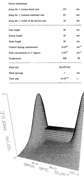
A planar GaAs MESFET has been simulated using the method described in the previous section. The gate length of the device was chosen to be 26 nm. GaAs MESFET’s, grown by MBE on semi-insulating substrates, with gate lengths as short as 27.5 f 2.5 nm have currently been fabricated [lo]. The lengths of the source and drain were considered to be both 24 nm. The complete list of device parameters used in our simulation is given in Table I. Physical parameters such as effective masses, valley sep- aration, phonon energies, etc., are given in [ 1 I].
The doping concentration of the nf contact regions is taken to be nonuniform (Gaussian-like) with a peak con- centration of 1 X l O I 7 ~ m - ~ . The incorporation of such a profile (representative of ion-implanted devices, although
unrealistically implemented in our simulation, with re-
spect to its actual spread), smoothes out the problems (i.e., spikes in the particle distribution) encountered at the boundaries of the much steeper, wall-like, doping profiles used in previous simulations [ 121. In addition, a higher, more realistic doping has not been considered since it ne- cessitates the use of the Pauli exclusion principle to take into account the degeneracy effect. The doping concen- tration of the conduction channel was taken to be uniform with a value of 2 X l o i 6 ~ m - ~ . The overall doping profile
considered in this simulation is shown in Fig. 1. During the initial time steps of the device operation (gate is “on”; see Fig. 2), thermally distributed electrons are injected at the source contact into the n+ region of the device. The outgoing components of the wavefunction are identified and removed at these contacts. However, the use of this kind of boundary conditions has been shown to lead to the development of “spikes” of the particle distribution at the contacts [ 121. In order to overcome this problem, we have kept the wave-function constant at these
1012 IEEE TRANSACTIONS ON ELECTRON DEVICES, VOL. 36, NO. 6, JUNE 1989
"1
TABLE IN U M E R I C A L A N D DEVICE PARAMETERS FOR A THREE-DIMENSIONAL TIME- DEPENDENT SIMULATION O F A PLANAR GaAs MESFET
-
3
Device dimensions:
along the - x (source-drain) axis 127 nm
along the -y (contacts-subsuate) axis 63 nm $ 0
r
6
ro
along the -z (width of the device) axis 16 nm
Gate length 26 nm Q
Source length 24 nm
Drain length
Channel doping concentration Peak concentration at n+ regions Temperature Mesh size 24 nm 2x10'~ cm-' 1x10" cm? 300 OK 63x127~16 1
Mesh spacings nm Fig. 2. Potential energy profile (as viewed from the contacts region) after
Time step 4~10-l~ s
-. .
the device has been switched on. The values of the potentials are V,,,,,,
= 0 v. V".,, = -0.3 v, V,+,," = 1 v .
0
Fig. 3 . Carrier density distribution in the device at time f = 4 fs (just before we switch the device off). Carriers in both
r
and L valleys have been taken into account ( I $ ( x ) 1' = I $ ( x ) 1; + I $(x) I;.). The external bias is that of Fig. 2.Fig. 1. Doping profile (normalized) used in our simulation. The dopant concentration at the peaks of the n + regions is taken to be 1 x 10'' ~ 3 1 7 ~ ~ .
The concentration in the conductive channel is 2 x 10l6 ~ m - ~ . In this graph, the device is viewed from the substrate region.
contacts after the first time steps. This is an ad hoc, but
reasonable, constraint.
The simulation was carried out on a 63 x 127 x 16
mesh (with 1-nm mesh spacing), with periodic boundary conditions in the --z direction (which represents the width of the device; see Table I), where translational invariance is expected. This choice of the mesh spacing satisfies the
sampling requirements [ 131 of the numerical method used,
and minimizes the numerical error due to the discretiza- tion of the kinetic energy operator [ 141. A time step of 4
x s has been used. With this time step, a simulation
corresponding to 1 ps takes approximately 70 h of com-
puter time (system units) on a CRAY X-MP (at present,
90 percent of the computer time is spent in the handling of the electron-phonon interaction; this amount will be considerably reduced in the future as the code is further optimized). We have, so far, performed runs out to 0.01 ps. Fig. 3 shows the carrier density distribution obtained at a time t = 4 fs after the device has been switched on
(V,,,, = - 0 . 3 V , Vdrain = 1 V , V,,,,,, = 0 V; see Fig. 2). After this time, the gate is instantaneously switched ("off
">
to V,,,, = 0.1 V (with Vdrain = 1 V and VS,,,, =YALABIK er al.: SIMULATION OF CHARGE TRANSPORT IN SEMICONDUCTOR STRUCTURES 1013
Fig. 4. Potential energy profile after the device has been switched off. The values of the potentials are V,<,uccc = -0.3 V, V,,,, = 0.1 V, Vd,,,, = 1 V.
Fig. 5 . Carrier density distribution at time t = 6.4 fs after the device has been switched off. The external bias is that of Fig. 4 . Notice the for- mation of a depletion layer manifested by the “pushing away” of the carrier density away from the gate contact.
distribution obtained at a time t = 6.4 fs after the gate
has been switched “off.” The early stage of the formation of the depletion layer can clearly be seen (manifested by the “pushing away” of the carrier density from the gate contact). These results, although preliminary, are indic- ative of the very fast switching times that are believed to characterize the short-channel (submicrometer and ultra- submicrometer gate) semiconductor devices. Work for the accurate estimation of the switching times of the device along with quantities such as charge and current distri-
and energy distributions in the
I?
and L valleys, is cur-rently under way and results will be reported soon.
IV. CONCLUSION
A three-dimensional quantum mechanical simulation method based on the solution of the coupled time-depen- dent Schrodinger and Poisson equations has been carried out for a planar ultrasubmicrometer gate GaAs MESFET and initial results of the device’s transient behavior have been presented. Charge transport in the
r
and L conduc-tion band valleys along with intravalley optical and acoustical, and intervalley (equivalent and nonequivalent) phonon scattering has been considered. The effects of phonons are included in an approximation that is consis- tent with the results of perturbation theory and yields the correct two-point time correlation function in equilib- rium. The results obtained indicate that very fast response times characterize such short-channel GaAs devices.
This type of simulation is expected to be particularly useful in the analysis and design of electronic devices with geometric feature sizes comparable to the quantum me- chanical wavelength of the carriers, a regime in which the semiclassical approaches are no longer valid and a more fundamental simulation method is needed.
REFERENCES
[ I ] D. J . Widiger, I. C. Kizilyalli, K. Hess, and J. J . Coleman, “Two- dimensional transient simulation of an idealized high electron mobil- ity transistor,” IEEE Trans. Electron Devices, vol. ED-32, pp. 1092-
1102, 1985.
[2] C . Jacoboni and L. Reggiani, “The Monte Carlo method for the so- lution of charge transport in semiconductors with applications to co- valent materials,” Rev. Mod. P h y s . , vol. 5 5 , pp. 645-705, 1983. [3] E. Wigner, “On the quantum correction for thermodynamic equilib-
rium,” Phys. R e v . , vol. 40, pp. 749-759, 1932.
[4] G . J . Iafrate, H . L. Grubin. and D. K. Ferry, “Utilization of quantum distribution functions for ultra-submicron device transport,” J . Phys.,
suppl. 10, vol. 42, pp. 307-312, 1981.
[ 5 ] G. J . Iafrate, “The physics of submicroniultrasubmicron dimen-
sions,’’ in Gallium Arsenide Technology, D. K. Ferry, Ed. Indi- anapolis, IN: H . W . Sams & CO, 1985, ch. 12.
161 K. K. Thornber and R. P. Feynman, “Velocity acquired by an elec- tron in a finite electric field in a polar crystal,” Phys. Rev. B . vol. 1. pp. 4099-41 14, 1970.
[7] A. 0. Caldeira and A. J . Leggett. “Quantum tunneling in a dissipa- tive system,” Ann. P h v s . , vol. 149, pp. 374-456, 1983.
[8] G. D. Mahan, “Quantum transport equation for electric and magnetic fields,” Phys. R e p . , vol. 145, pp. 251-318, 1987.
191 A. P. Jauho and J. W. Wilkins, “Theory of high-electric-field quan- tum transport for electron-resonant impurity systems,’’ Phys. Rev. B . vol. 29, pp. 1919-1938, 1984.
[IO] G. Bernstein and D. K . Ferry, “Electron beam lithographic fabrica- tion of ultra-submicron gate GaAs MESFETs, ” Superlattices and Mi-
crostructures, vol. 2 , pp. 147-150, 1986.
(111 M . A . Littlejohn, J. R . Hauser, and T . H. Glisson, “Velocity-field characteristics of GaAs with rz-L;-Xz conduction band ordering,” J .
1121 M. C. Yalabik, J . D. Gunton, G. Neofotistos, and K. Diff, “Simu- lation of charge transport in a GaAs MESFET using the time depen- dent Schrodinger equation,” Superlattices and Microstructures, vol. 3 , pp.463-465, 1987.
[I31 W. H . Press, B . P. Flannery, S . A. Teukolsky, and W . T. Vetterling,
Numerical Recipes.
[14] R. B . Gerber, R . Kosloff, and M . Berman, “Time-dependent wave- oacket calculations of molecular scattering from surfaces.” Comn.
Appl. P h y s . , vol. 48, pp. 4587-4590, 1977.
New York: Cambridge, 1986, p. 386.
v
IEEE TRANSACTIONS ON ELECTRON DEVICES, VOL. 36, NO. 6, JUNE 1989 1014
M. C. Yalabik, photograph and biography not available at the time of Hong Guo received the B S degree in physics
publication from the Sichuan Normal University, and the
Ph D degree in physics from the Uniersity of His research work has included studies on crit-
*
Pittsburgh in 1987ical phenomena, finite-size scaling. and renor- G. Neofotistos received the B A. degree in phys- malization group theories. He is currently inter- ics from the University of Athens, Greece, in ested in quantum transport theory and 1985. He is working toward the Ph.D. degree in nonequilibrium statistical physics
physics at Temple University, Philadelphia, PA. His dissertation is entitled “Quantum Transport
in Submicron Semiconductor Electronic De-
*
vices.” He is currently conducting research in resonant tunneling in heterojunction structures, device modeling, quantum interference struc- tures, and quantum transport in submicrometer and nanometer-scale GaAs devices.
*
Karim Diff received the B . S . degree in physics from the University of Algiers in 1982, and the M . S . degree in physics from the University of Pennsylvania in 1985. He is currently working to- ward the Ph.D. degree in physics at Temple Uni- versity, Philadelphia, PA. His dissertation will be on quantum charge transport in resonant tunneling heterostructures and he is currently interested in space-charge effects on resonant tunneling, time- modulated barriers, and the energy-loss rates of camers in quantum wells.
James D. Gunton (M’88) received the B A de- gree in physics from Oxford University (Rhodes Scholar) in 1961 and the Ph D degree i n physics from Stanford University in 1967.
In 1968, he joined the Department of Physics at Temple University where he was a Professor and Director of the Center for Advanced Com- putational Science, until July 1988, when he joined Lehigh University as Dean of Arts and Sci- ence. His research interests have included renor- malization group theories, nonlinear phenomena far from equilibrium, critical dynamics, surface phase transitions, dynam- ics of metastable and unstable states, finite-size effects, and molecular dy- namic< simulations of crystal growth His current research interests are i n
nonequilibrium statistical physics and quantum transport theory Dr Gunton is a member of the American Physical Society, the New York Academy of Sciences, Sigma Xi, and has served in the Federal Co- ordinating Council on Science, Engineering and Technology Committee on Supercomputing, and the NSF Advisory Panel on Computational Mathe- matics.