Improved InGaN/GaN light-emitting diodes with
a p-GaN/n-GaN/p-GaN/n-GaN/p-GaN
current-spreading layer
Zi-Hui Zhang,1 Swee Tiam Tan,1 Wei Liu,1 Zhengang Ju,1 Ke Zheng,1 Zabu Kyaw,1 Yun Ji,1 Namig Hasanov,1 Xiao Wei Sun1,2,5 and Hilmi Volkan Demir1,3,4,6
1LUMINOUS! Center of Excellence for Semiconductor Lighting and Displays, School of Electrical and Electronic
Engineering, Nanyang Technological University, 50 Nanyang Avenue, 639798, Singapore
2South University of Science and Technology, 1088 Xue-Yuan Road, Shenzhen, Guangdong, 518055, China 3School of Physical and Mathematical Sciences, Nanyang Technological University, 50 Nanyang Avenue, 639798,
Singapore
4Department of Electrical and Electronics, Department of Physics, and UNAM-Institute of Material Science and
Nanotechnology, Bilkent University, TR-06800, Ankara, Turkey
5[email protected] 6[email protected]
Abstract: This work reports both experimental and theoretical studies on
the InGaN/GaN light-emitting diodes (LEDs) with optical output power and external quantum efficiency (EQE) levels substantially enhanced by incorporating p-GaN/n-GaN/p-GaN/n-GaN/p-GaN (PNPNP-GaN) current spreading layers in p-GaN. Each thin n-GaN layer sandwiched in the PNPNP-GaN structure is completely depleted due to the built-in electric field in the PNPNP-GaN junctions, and the ionized donors in these n-GaN layers serve as the hole spreaders. As a result, the electrical performance of the proposed device is improved and the optical output power and EQE are enhanced.
©2013 Optical Society of America
OCIS codes: (230.3670) Light-emitting diodes; (230.5590) Quantum-well, -wire, and -dot devices; (160.6000) Semiconductor materials.
References and links
1. S. T. Tan, X. W. Sun, H. V. Demir, and S. P. DenBaars, “Advances in the LED materials and architectures for energy-saving solid-state lighting toward “lighting revolution”,” IEEE Photon. J. 4(2), 613–619 (2012). 2. M. H. Crawford, “LEDs for solid-state lighting: performance challenges and recent advances,” IEEE J. Sel. Top.
Quantum Electron. 15(4), 1028–1040 (2009).
3. N. Tansu, H. Zhao, G. Liu, X. H. Li, J. Zhang, H. Tong, and Y. K. Ee, “III-nitride photonics,” IEEE Photon. J. 2(2), 241–243 (2010).
4. R. M. Farrell, E. C. Young, F. Wu, S. P. Denbaars, and J. S. Speck, “Materials and growth issues for high-performance nonpolar and semipolar light-emitting devices,” Semicond. Sci. Technol. 27(2), 024001–024014 (2012).
5. D. A. Browne, E. C. Young, J. R. Lang, C. A. Hurni, and J. S. Speck, “Indium and impurity incorporation in InGaN films on polar, nonpolar, and semipolar GaN orientations grown by ammonia molecular beam epitaxy,” J. Vac. Sci. Technol. A 30(4), 041513–041520 (2012).
6. H. Zhao, G. Liu, J. Zhang, J. D. Poplawsky, V. Dierolf, and N. Tansu, “Approaches for high internal quantum efficiency green InGaN light-emitting diodes with large overlap quantum wells,” Opt. Express 19(S4 Suppl 4), A991–A1007 (2011).
7. J. Zhang and N. Tansu, “Improvement in spontaneous emission rates for InGaN quantum wells on ternary InGaN substrate for light-emitting diodes,” J. Appl. Phys. 110(11), 113110 (2011).
8. H. P. Zhao, G. Y. Liu, X. H. Li, R. A. Arif, G. S. Huang, J. D. Poplawsky, S. Tafon Penn, V. Dierolf, and N. Tansu, “Design and characteristics of staggered InGaN quantum-well light-emitting diodes in the green spectral regime,” IET Optoelectron. 3(6), 283–295 (2009).
9. H. Zhao, G. Liu, and N. Tansu, “Analysis of InGaN-delta-InN quantum wells for light-emitting diodes,” Appl. Phys. Lett. 97(13), 131114 (2010).
10. Y. K. Ee, J. M. Biser, W. Cao, H. M. Chan, R. P. Vinci, and N. Tansu, “Metalorganic vapor phase epitaxy of III-nitride light-emitting diodes on nanopatterned AGOG sapphire substrate by abbreviated growth mode,” IEEE J. Sel. Top. Quantum Electron. 15(4), 1066–1072 (2009).
#178005 - $15.00 USD Received 12 Oct 2012; revised 5 Feb 2013; accepted 7 Feb 2013; published 21 Feb 2013
11. Y. K. Ee, X. H. Li, J. Biser, W. Cao, H. M. Chan, R. P. Vinci, and N. Tansu, “Abbreviated MOVPE nucleation of III-nitride light-emitting diodes on nano-patterned sapphire,” J. Cryst. Growth 312(8), 1311–1315 (2010). 12. Y. Li, S. You, M. Zhu, L. Zhao, W. Hou, T. Detchprohm, Y. Taniguchi, N. Tamura, S. Tanaka, and C. Wetzel,
“Defect-reduced green GaInN/GaN light-emitting diode on nanopatterned sapphire,” Appl. Phys. Lett. 98(15), 151102 (2011).
13. H. Zhao, G. Liu, R. A. Arif, and N. Tansu, “Current injection efficiency induced efficiency-droop in InGaN quantum well light-emitting diodes,” Solid-State Electron. 54(10), 1119–1124 (2010).
14. J. Wang, L. Wang, Z. Hao, Y. Luo, A. Dempewolf, M. Müller, F. Bertram, and J. Christen, “An improved carrier rate model to evaluate internal quantum efficiency and analyze efficiency droop origin of InGaN based light-emitting diodes,” J. Appl. Phys. 112(2), 023107 (2012).
15. H. J. Kim, S. Choi, S. S. Kim, J. H. Ryou, P. D. Yoder, R. D. Dupuis, A. M. Fischer, K. Sun, and F. A. Ponce, “Improvement of quantum efficiency by employing active-layer-friendly lattice-matched InAlN electron blocking layer in green light-emitting diodes,” Appl. Phys. Lett. 96(10), 101102 (2010).
16. N. Tansu and L. J. Mawst, “Current injection efficiency of InGaAsN quantum-well lasers,” J. Appl. Phys. 97(5), 054502 (2005).
17. H. Kim, S. J. Park, and H. Hwang, “Effects of current spreading on the performance of GaN-based light-emitting diodes,” IEEE Trans. Electron. Dev. 48(6), 1065–1069 (2001).
18. R. M. Lin, Y. C. Lu, Y. L. Chou, G. H. Chen, Y. H. Lin, and M. C. Wu, “Enhanced characteristics of blue InGaN/GaN light-emitting diodes by using selective activation to modulate the lateral current spreading length,” Appl. Phys. Lett. 92(26), 261105 (2008).
19. T. W. Kuo, S. X. Lin, P. K. Hung, K. K. Chong, C. I. Hung, and M. P. Houng, “Formation of selective high barrier region by inductively coupled plasma treatment on GaN-based light-emitting diodes,” Jpn. J. Appl. Phys. 49(11), 116504 (2010).
20. H. Y. Ryu and J. I. Shim, “Effect of current spreading on the efficiency droop of InGaN light-emitting diodes,” Opt. Express 19(4), 2886–2894 (2011).
21. D. Han, J. Shim, D. S. Shin, E. Nam, and H. Park, “Effect of temperature distribution and current crowding on the performance of lateral GaN-based light-emitting diodes,” Phys. Status Solidi C 7(7-8), 2133–2135 (2010). 22. E. F. Schubert, Light-Emitting Diodes, 2nd ed. (Cambridge University Press, 2006).
23. C. F. Tsai, Y. K. Su, and C. L. Lin, “Improvement in the light output power of GaN-based light-emitting diodes by natural-cluster silicon dioxide nanoparticles as the current-blocking layer,” IEEE Photon. Technol. Lett. 21(14), 996–998 (2009).
24. J. H. Son, B. J. Kim, C. J. Ryu, Y. H. Song, H. K. Lee, J. W. Choi, and J.-L. Lee, “Enhancement of wall-plug efficiency in vertical InGaN/GaN LEDs by improved current spreading,” Opt. Express 20(S2 Suppl 2), A287– A292 (2012).
25. H. H. Liu, P. R. Chen, G. Y. Lee, and J. I. Chyi, “Efficiency enhancement of InGaN LEDs with an n-type AlGaN/GaN/InGaN current spreading layer,” IEEE Electron Device Lett. 32(10), 1409–1411 (2011). 26. S. R. Jeon, Y. H. Song, H. J. Jang, G. M. Yang, S. W. Hwang, and S. J. Son, “Lateral current spreading in
GaN-based light-emitting diodes utilizing tunnel contact junctions,” Appl. Phys. Lett. 78(21), 3265–3267 (2001). 27. A. H. Reading, J. J. Richardson, C. C. Pan, S. Nakamura, and S. P. DenBaars, “High efficiency white LEDs with
single-crystal ZnO current spreading layers deposited by aqueous solution epitaxy,” Opt. Express 20(1 S1), A13–A19 (2012).
28. V. K. Malyutenko, S. S. Bolgov, and A. N. Tykhonov, “Research on electrical efficiency degradation influenced by current crowding in vertical blue InGaN-on-SiC light-emitting diodes,” IEEE Photon. Technol. Lett. 24(13), 1124–1126 (2012).
29. C.-K. Li and Y.-R. Wu, “Study on the current spreading effect and light extraction enhancement of vertical GaN/InGaN LEDs,” IEEE Trans. Electron. Dev. 59(2), 400–407 (2012).
30. Z. G. Ju, S. T. Tan, Z.-H. Zhang, Y. Ji, Z. Kyaw, Y. Dikme, X. W. Sun, and H. V. Demir, “On the origin of the redshift in the emission wavelength of InGaN/GaN blue light emitting diodes grown with a higher temperature interlayer,” Appl. Phys. Lett. 100(12), 123503 (2012).
31. Z. -H. Zhang, S. T. Tan, Z. Ju, W. Liu, Y. Ji, Z. Kyaw, Y. Dikme, X. W. Sun and H. V. Demir, “On the effect of step-doped quantum barriers in InGaN/GaN light emitting diodes,” IEEE/OSA J. Display Technol. PP(99), 1–8 (2012).
32. M. Meneghini, N. Trivellin, G. Meneghesso, E. Zanoni, U. Zehnder, and B. Hahn, “A combined electro-optical method for the determination of the recombination parameters in InGaN-based light-emitting diodes,” J. Appl. Phys. 106(11), 114508 (2009).
33. J. Piprek, “Efficiency droop in nitride-based light-emitting diodes,” Phys. Status Solidi., A Appl. Mater. Sci. 207(10), 2217–2225 (2010).
34. V. Fiorentini, F. Bernardini, and O. Ambacher, “Evidence for nonlinear macroscopic polarization in III-V nitride alloy heterostructures,” Appl. Phys. Lett. 80(7), 1204–1206 (2002).
35. I. Vurgaftman and J. R. Meyer, “Band parameters for nitrogen-containing semiconductors,” J. Appl. Phys. 94(6), 3675–3696 (2003).
36. S. M. Sze, Physics of Semiconductor Devices, 2nd ed. (John Wiley & Sons, Inc., 1981).
37. K. Kumakura, T. Makimoto, N. Kobayashi, T. Hashizume, T. Fukui, and H. Hasegawa, “Minority carrier diffusion length in GaN: dislocation density and doping concentration dependence,” Appl. Phys. Lett. 86(5), 052105 (2005).
#178005 - $15.00 USD Received 12 Oct 2012; revised 5 Feb 2013; accepted 7 Feb 2013; published 21 Feb 2013
38. B. J. Baliga, Fundamentals of Power Semiconductor Devices (Springer Science + Business Media, LLC, 2008). 39. M. K. Kwon, I. K. Park, J. Y. Kim, J. O. Kim, B. Kim, and S. J. Park, “Gradient doping of Mg in p-type GaN for
high efficiency InGaN-GaN ultraviolet light-emitting diode,” IEEE Photon. Technol. Lett. 19(23), 1880–1882 (2007).
40. D. K. Schroder, Semiconductor Material and Device Characterization, 2nd ed. (John Wiley & Sons, Inc., 1998). 41. Y. J. Liu, C. C. Huang, T. Y. Chen, C. S. Hsu, J. K. Liou, and W. C. Liu, “Improved performance of an
InGaN-based light-emitting diode with a p-GaN/n-GaN barrier junction,” IEEE J. Quantum Electron. 47(6), 755–761 (2011).
42. V. K. Malyutenko, S. S. Bolgov, “Effect of current crowding on the ideality factor in MQW InGaN/GaN LEDs on sapphire substrates,” Proc. SPIE 7617, 76171K −76171K–9 (2010).
43. Z. Gong, S. Jin, Y. Chen, J. McKendry, D. Massoubre, I. M. Watson, E. Gu, and M. D. Dawson, “Size-dependent light output, spectral shift, and self-heating of 400 nm InGaN light-emitting diodes,” J. Appl. Phys. 107(1), 013103 (2010).
44. Y. C. Shen, G. O. Mueller, S. Watanabe, N. F. Gardner, A. Munkholm, and M. R. Krames, “Auger recombination in InGaN measured by photoluminescence,” Appl. Phys. Lett. 91(14), 141101 (2007).
1. Introduction
InGaN/GaN light-emitting diodes (LEDs) are regarded as the most promising lighting sources of the next generation [1–3]. However, there are currently still some limiting factors for achieving high performance InGaN quantum well (QW) LEDs. Those factors typically include the charge separation in QWs [4–9], the high dislocation density [10–12] that limits the internal quantum efficiency (IQE), and the carrier leakage process that leads to the efficiency-droop [13–15]. Recent methods based on semi/non-polar QWs [4,5], polar QWs with a large overlap of the electron-hole wave functions [6–9], and epi-growth on nano-patterned sapphires [10–12] have led to the improved IQE in InGaN-based LEDs. The suppression of the thermionic carrier leakage in InGaN QWs has also resulted in the droop suppression [13–15], which is consistent with the general theory of the current injection efficiency in QW lasers / LEDs [16].
Meanwhile, besides the technical issues in charge separation, carrier injection/confinement efficiency and the crystal quality of the QWs, the current crowding at the p-contact is also regarded as one of the main obstacles [17–19], especially for conventional devices grown on insulating substrates (e.g., sapphire) [20]. The driven current tends to flow through the path with smaller resistivity, resulting in current crowding at the p-contact of these InGaN/GaN LEDs. The current crowding effect generates highly localized carrier density and heat underneath the p-electrode and thus leads to a non-uniform light emission of the InGaN/GaN LEDs [21]. In order to improve the current spreading, a resistive layer is generally added into the LED architecture [22]. For example, Tsai et. al. has proposed a current blocking layer formed by silicon dioxide nanoparticles [23] and the patterned Al2O3 on p-GaN for a better current spreading [24], while n-type InGaN was also proposed and inserted underneath the InGaN/GaN active region to improve the current spreading [25]. On the other hand, tunneling junction has also been proposed as a current spreading layer [26]. Most recently, more efforts have been invested to the single-crystal ZnO as the current spreading layer [27]. In addition, the use of vertical LEDs has also been investigated for suppressing the current crowding in nitride-based LEDs [24, 28,29]. In this work, we propose and demonstrate a lattice-matched p-GaN/n-GaN/p-GaN/n-GaN/p-GaN (PNPNP-GaN) epitaxial current spreading layer in the p-type cap region of InGaN/GaN LEDs. In these devices, with this PNPNP-GaN epi-structure, the electrical performance is also improved. Further enhancement of the optical output power and external quantum efficiency (EQE) has also been achieved, which is attributed to the improved current spreading effect in the proposed epi-structure.
2. Experiments
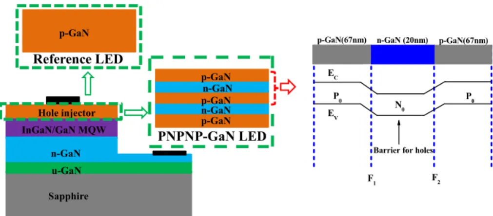
In our study, two sets of InGaN/GaN LED wafers (i.e., Reference LED and PNPNP-GaN LED sketched in Fig. 1) were grown by an AIXTRON close-coupled showerhead metal-organic chemical vapour deposition (MOCVD) reactor on c-plane patterned-sapphire #178005 - $15.00 USD Received 12 Oct 2012; revised 5 Feb 2013; accepted 7 Feb 2013; published 21 Feb 2013
substrates [30]. In our experiment, TMGa/TEGa/TMIn and NH3 were used as the group-III sources and the group-V sources, respectively. Diluted Cp2Mg and SiH4 were used as the dopant precursors for p-type and n-type GaN, respectively. The growth was initiated from a 30 nm low-temperature GaN buffer layer, then followed by a 2 µm u-GaN layer and a 4 µm n-GaN layer (Nd = 5 × 1018 cm−3), which were both grown at 1050 °C. In the grown LED epi-samples, the active layer consists of five-period In0.15Ga0.75N/GaN multiple quantum wells (MQWs), with well and barrier thickness of 3 nm and 12 nm, respectively. The wells and barriers were grown at the same temperature of 730 °C. The Reference LED has a 0.2 µm thick p-GaN layer with a hole concentration of 3 × 1017 cm−3. By inserting two 20 nm n-GaN (Nd = 2 × 1017 cm−3) layers into p-GaN layer evenly, we obtained the PNPNP-GaN structure (0.067 µm /20 nm /0.067 µm /20 nm /0.067 µm) with the same thickness of the p-GaN layer in the reference device. The PNPNP-GaN layers were all grown at 1020 °C, which was lower than the temperature (1050 °C) used for the growth of u-GaN and n-GaN layers to suppress the out-diffusion of the InN from the InGaN quantum wells. Specifically, the growth pressure for the n-GaN and p-GaN in the PNPNP-GaN structure was set to 150 mbar. The V/III ratio (NH3/TMGa) during PNPNP-GaN growth was kept to be 4100. After the epi-wafers were grown, we performed the thermal annealing to activate the Mg dopants for p-GaN layers. The annealing was conducted for 10 min in the ambient of N2 at a temperature of 720 °C for both the Reference LED and PNPNP-GaN LED wafers.
EV EC
F2
N0 P0
P0
Barrier for holes
F1
p-GaN(67nm) n-GaN (20nm) p-GaN(67nm)
p-GaN Reference LED p-GaN n-GaN p-GaN n-GaN p-GaN PNPNP-GaN LED Sapphire u-GaN InGaN/GaN MQW Hole injector n-GaN
Fig. 1. Schematic diagrams of the studied devices (Reference LED without ITO coating and PNPNP-GaN LED without ITO coating), shown along with the band diagram of one PNP-GaN junction in the PNPNP-GaN LED.
After the LED wafers were grown, four sets of LED chips were fabricated by following the standard fabrication process. The epi-wafers were patterned into mesas of size 350 µm × 350 µm through reactive ion etch (RIE). Ni/Au film (10 nm/150 nm) was first deposited as the p-electrode, and then the p-contact was annealed in the mixture of O2 and N2 at 515 °C for 5 min under the atmosphere pressure. Finally, Ti/Au (30 nm/150 nm) was deposited as the n-electrode. We have prepared two sets of devices without indium tin oxide (ITO) coating (i.e., the Reference LED without ITO and PNPNP-GaN LED without ITO). The other two sets were prepared with ITO coating as the transparent current spreading layer (i.e., Reference LED with ITO and PNPNP-GaN LED with ITO, which are shown in the supplementary material). The transparent current spreading layer (i.e., ITO) was sputtered and annealed in the ambient of N2 at 500 °C for 120 s before depositing electrodes. Also, we performed numerical simulations for the four sets of devices in APSYS [31], which solves the Poisson equation, continuity equation and Schrödinger equation with proper boundary conditions. The Auger recombination coefficient used in these simulations was 1 × 10⁻³⁰ cm6s−1 [32], and the
#178005 - $15.00 USD Received 12 Oct 2012; revised 5 Feb 2013; accepted 7 Feb 2013; published 21 Feb 2013
energy band offset between the conduction band and the valence band was 70/30 [33]. Considering the crystal relaxation by generating dislocations, 40% of the theoretical polarization charge was assumed [34]. Other parameters can be found elsewhere [35].
3. Results and discussion
As indicated in Fig. 1, the PNPNP-GaN LEDs (i.e., PNPNP-GaN LED without ITO and PNPNP-GaN LED with ITO) own two layers of thin n-GaN (20 nm), sandwiched between 67 nm thick p-GaN layers. Each thin n-GaN forms two junctions at the interfaces (i.e., F1 and F2). When the InGaN/GaN LED is forward biased, F1 is also forward biased, whereas F2 is reversely biased. As the applied bias increases, the depletion region of F1 shrinks, while F2 extends its depletion region across the GaN. Thereby, the depletion region in the entire n-GaN layer can be retrieved, thus with the ionized Si donors here acting as the hole spreaders. With the doping concentration of n-GaN (2 × 1017 cm−3) and p-GaN (3 × 1017 cm−3), the
built-in potential built-in the p-GaN/n-GaN is 3.23 V ( ln A2D
bi i N N kT V e n = , e is the elementary
electronic charge, and ni = 1.9 × 10⁻¹⁰ cm−3 for GaN). The total depletion region thickness is
162.83 nm ( 2 r 0 A D T bi A D N N W V e N N ε ε + =
, εr = 8.9 for GaN, and εo is the absolute dielectric
constant) [36], which consists of the depletion region in n-GaN and p-GaN of 97.70 and 65.13 nm, respectively, provided that n-GaN and p-GaN have infinite lengths. Therefore, the n-GaN layer, which has a thickness of only 20 nm, is fully depleted in PNPNP-GaN LEDs. Meanwhile, according to the principle of charge neutrality in the depletion region of a homojunction, the actual depletion width in p-GaN of the PNP-GaN junction is only about 13.33 nm. On the other hand, the diffusion length (LD) of holes in the n-GaN can be obtained by using LD= Dp pτ = kTμp/eτp (where Dp is the diffusion constant of holes, correlated
with µp by Einstein relationship, and k is the Boltzman constant). Here, the minority carrier (hole) lifetime in n-GaN with a doping concentration of 2 × 1017 cm−3 is assumed to be 0.8 ns, while the hole mobility is set to be 26 cm2/Vs [37]. Thus, the diffusion length for holes is calculated to be ~231.9 nm, which is much larger than the thickness of n-GaN (20 nm) in each PNP-GaN junction of the PNPNP-GaN LED. As a result, there will be no hole loss across the n-GaN region. Furthermore, there exists a reach-through breakdown voltage for the reversely biased junction (i.e., F2), and the reach-through breakdown voltage is 0.08V in this case ( 0 2 D N RT r eN W BV ε ε
= , and WN is the width of n-GaN) [38]. It is worth mentioning that this
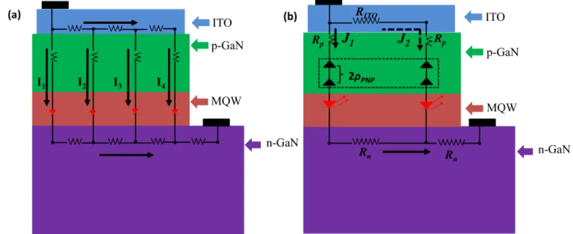
BVRT is smaller than the built-in potential within the p-GaN/n-GaN junctions, and this also manifests itself in the full depletion of n-GaN by leaving behind ionized Si dopants as the hole spreaders. Therefore, after the depletion region extends through the whole n-GaN region, any increase in the applied bias will promote the injection of minority carriers (i.e., holes in our case) from the forward biased junction (i.e., F1) to produce a high-current flow. For InGaN/GaN LEDs grown on insulating substrates with lateral current-injection scheme, the current travels both vertically and laterally as indicated in Fig. 2(a). As the sheet resistance of n-GaN is much smaller than the sheet resistance of p-GaN, the current tends to flow through the low-resistivity n-GaN layer (Fig. 2(a)), giving a non-uniform current distribution in p-GaN (i.e., I1 > I2 > I3 > I4 > ... > In), well known as the current crowding effect [22]. This current crowding effect can be suppressed if PNPNP-GaN is employed in the LED architecture. A simplified equivalent circuit of InGaN/GaN LEDs with the embedded PNPNP-GaN homojunctions is depicted in Fig. 2(b), in which the total current is divided into vertical current (J1) and horizontal current (J2). The total voltage drop consists of those in the
#178005 - $15.00 USD Received 12 Oct 2012; revised 5 Feb 2013; accepted 7 Feb 2013; published 21 Feb 2013
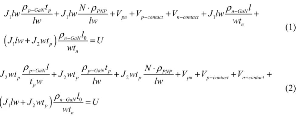
p-contact, p-GaN, MQW region, n-GaN as well as n-contact. Based on the equivalent circuit in Fig. 2(b), Eq. (1) (for current path 1) and Eq. (2) (for current path 2) are obtained.
(
)
1 1 1 0 1 2 p GaN p PNP n GaN pn p contact n contact n n GaN p n t N l J lw J lw V V V J lw lw lw wt l J lw J wt U wt ρ ρ ρ ρ − − − − − ⋅ + + + + + + + = (1)(
)
2 2 2 0 1 2 p GaN p GaN p PNP p p p pn p contact n contact p n GaN p n l t N J wt J wt J wt V V V t w lw lw l J lw J wt U wt ρ ρ ρ ρ − − − − − ⋅ + + + + + + + = (2)where l represents the length of the lateral current path, l0 is the distance from the mesa edge to the center of the n-contact, and w is the length of the stripped contact. The thickness of p-GaN and n-p-GaN is tp and tn, respectively; ρp-GaN and ρn-GaN is the resistivity for p-GaN and n-GaN, respectively; Vpn denotes the junction voltage drop of multiple quantum wells in InGaN/GaN LED; and Vp-contact and Vn-contact are the voltage drops across the p-contact and n-contact, respectively. ρPNP is the specific interfacial resistivity induced by the barrier height in each PNP-GaN junction. N is the total number of PNP-GaN junction, and in our device, there are two PNP-GaN junctions (i.e., PNPNP-GaN), and thus N is 2 (i.e., the total interfacial specific resistivity is 2 × ρPNP). VVV VVV VVV VVV VVV VVV VVV p-GaN MQW n-GaN p-GaN MQW n-GaN I1 I2 I3 I4 (a) VVVVVV VV VV VVVVVV Rp Rp Rn VVVVVV Rn J1 J2 VV VV VV VV 2ρPNP (b)
Fig. 2. (a) Equivalent circuit of an InGaN/GaN LED grown on an insulating substrate (e.g., sapphire) with lateral current-injection scheme (I1 > I2 > I3 > I4 > ... > In), and (b) a simplified
equivalent circuit of this InGaN/GaN LED with possible current paths (J1 and J2) when a PNPNP-GaN current spreading layer is embedded. ITO is not used in these two devices.
By equating Eq. (1) and Eq. (2), Eq. (3) is derived. However, l is in the order of device mesa size, which is 350 µm × 350 µm, while tp is the scale of p-GaN thickness, which is ~200 nm. Since tp << l, then Eq. (3) can be simplified into Eq. (4).
1 2 p PNP p p GaN t J l N J t ρ l ρ − = ⋅ + + (3)
#178005 - $15.00 USD Received 12 Oct 2012; revised 5 Feb 2013; accepted 7 Feb 2013; published 21 Feb 2013
1 2 PNP p p GaN J l N J t ρ ρ − ≅ ⋅ + (4)
Equation (4) shows that a higher ratio of N⋅ρPNP/ρp GaN− is beneficial for enhancing the lateral current (i.e., J2). To increase the ratio of N⋅ρPNP/ρp GaN− , either N⋅ρPNP has to be
increased or ρp GaN− has to be reduced. It is also feasible to increase the lateral current flow by increasing the p-GaN layer thickness (tp).
Furthermore, the PNPNP-GaN will not have very abrupt interfaces because of the dopant diffusion, especially the Mg diffusion [39]. However, one still can maintain the PNPNP-GaN junctions by properly increasing the Si doping concentration and/or the n-GaN thickness. Through this, the junction barrier (i.e., ρPNP) in each PNP-GaN can be formed, and Eq. (3), Eq. (4), Eq. (8) and Eq. (9) are still valid to explain the current spreading. Meanwhile, the n-GaN doping and n-n-GaN thickness have to follow the design guidelines, which were addressed previously, such that n-GaN has to be completely depleted and the reversed junction F2 will not block any current.
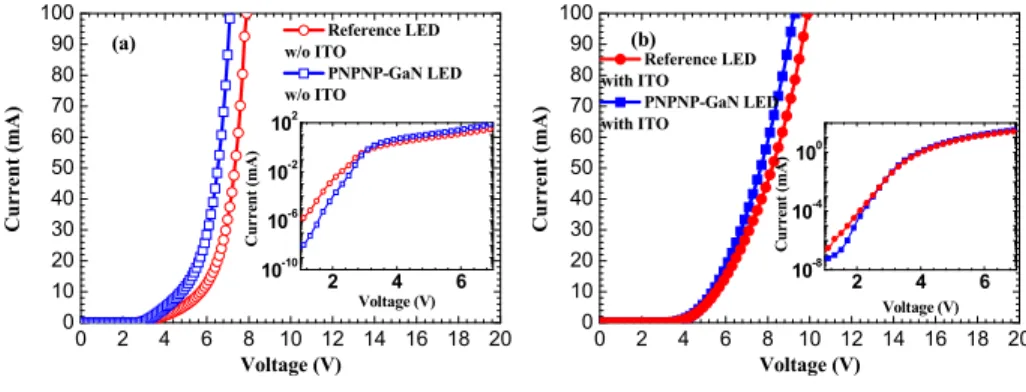
In order to probe the embedded PNPNP-GaN in terms of spreading current, we present the current as a function of voltage, as shown in Figs. 3(a) and 3(b). In the low forward voltage regime (0 ~3V in Figs. 3(a) and 3(b)), the PNPNP-GaN LED without ITO coating exhibits lower leakage current with respect to the Reference LED without ITO film in Fig. 3(a), while the same conclusion can be made for PNPNP-GaN LED with ITO coating with respect to its Reference LED with ITO according to Fig. 3(b). The Reference LEDs (i.e., Reference LEDs without and with ITO) and PNPNP-GaN LEDs (i.e., PNPNP-GaN LEDs without and with ITO) have the similar crystal quality, as their full-width at half-maximum (FWHM) of (102) and (002) X-ray diffraction spectra are both about 213.5 and 216.0 arcsec, respectively. Thus the suppressed leakage current in PNPNP-GaN LEDs comes from the increased junction barrier height. As the PNPNP-GaN junctions are embedded in such InGaN/GaN LEDs with multiple heterojunctions, it is therefore difficult to extract the barrier height for PNPNP-GaN. Here, we calculate the effective overall barrier height by the following,
2 ln , with eV nkT B s s kT A T I I e e I φ = = (5)
where ØB is the overall barrier height within the LED device, and n is the ideality factor for the diodes [40, 41]. ØB is calculated to be 1.10V for Reference LED without ITO and 1.31V for PNPNP-GaN LED without ITO, respectively. It is clearly revealed that a higher overall barrier height is obtained when PNPNP-GaN feature is integrated in the p-type layer. The ideality factor is 5.32 and 4.19 for Reference LED without ITO and PNPNP-GaN LED without ITO, respectively. An improved current spreading in PNPNP-GaN LED is responsible for the reduced ideality factor [42]. Furthermore, because of the improved current spreading effect in PNPNP-GaN LED without ITO, the electrical performance is improved compared to Reference LED without ITO when the applied bias is higher than 3V. Similarly,
ØB is determined to be 1.33V for Reference LED with ITO and 1.44V for PNPNP-GaN LED
with ITO, respectively. Moreover, the ideality factor is 6.52 and 4.51 for Reference LED with ITO and PNPNP-GaN LED with ITO, respectively. We also observed the increased overall energy barrier height in PNPNP-GaN LED with ITO, which in the meanwhile features the reduced ideality factor and the improved electrical properties compared to those in Reference LED with ITO. This is well attributed to the improved current spreading effect by the incorporation of PNPNP-GaN homojunctions.
#178005 - $15.00 USD Received 12 Oct 2012; revised 5 Feb 2013; accepted 7 Feb 2013; published 21 Feb 2013
0 2 4 6 8 10 12 14 16 18 20 0 10 20 30 40 50 60 70 80 90 100 2 4 6 10-10 10-6 10-2 102 Cu rr en t (mA) Voltage (V)
(a) w/o ITO Reference LED
PNPNP-GaN LED w/o ITO Curren t (mA) Voltage (V) 0 2 4 6 8 10 12 14 16 18 20 0 10 20 30 40 50 60 70 80 90 100 2 4 6 10-8 10-4 100 C urr ent ( m A ) Voltage (V) (b) Reference LED with ITO PNPNP-GaN LED with ITO Curren t (mA) Voltage (V)
Fig. 3. Liner-plot of experimentally measured current as a function of the applied voltage for (a) Reference LED without ITO coating and PNPNP-GaN LED without ITO coating (along with a semi-log plot inserted in the inset) and (b) Reference LED with ITO coating and PNPNP-GaN LED with ITO coating (again with a semi-log plot given in the inset).
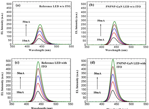
The electroluminescence (EL) spectra (Figs. 4(a), 4(b), 4(c) and 4(d)) were collected under 10, 20, 30, 40 and 50 mA of the injection current for both Reference LEDs without and with ITO and PNPNP-GaN LEDs without and with ITO. Both the EL spectra of Reference LED without ITO and PNPNP-LED without ITO in Figs. 4(a) and 4(b) show a red shift as the injection current level increases, which is due to a gradually increasing junction temperature during testing [43]. However, a less pronounced red shift observed in the EL spectra of Reference LED with ITO and PNPNP-LED with ITO in Figs. 4(c) and 4(d) is attributed to the significantly improved current spreading after ITO incorporation, which suppresses the high local heat caused by current crowding [21]. We can also see the EL intensity of PNPNP-GaN LEDs without and with ITO is enhanced compared to that of Reference LEDs without and with ITO, respectively. We also measured the integrated optical output power and EQE (Fig. 5(a)), which is compared with the simulated results for the four sets of studied devices (Fig. 5(b)). We can see an improved optical output power and EQE for PNPNP-GaN LEDs without and with ITO in both experiments and simulations. Compared to Reference LED without ITO in Fig. 5(a), PNPNP-GaN LED without ITO shows a power enhancement of 10.19% and 12.16% at 20 mA and 100 mA, respectively, while PNPNP-GaN LED with ITO enhances the output power by 16.98% and 14.37% at 20 mA and 100 mA, respectively compared to Reference LED with ITO. The improved device performance in PNPNP-GaN LEDs without and with ITO is attributed to the reduced current crowding effect. This in turn suppresses the high local carrier concentration, resulting in the reduced non-radiative Auger recombination in the multiple quantum wells [44].
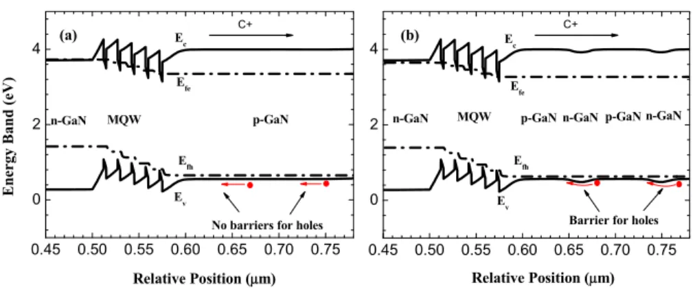
The energy band diagrams of Reference LEDs (i.e., Reference LED without and with ITO) and PNPNP-GaN LEDs (i.e., PNPNP-GaN LED without and with ITO) are shown in Figs. 6(a) and 6(b), respectively. The holes in the Reference LEDs experience no barriers when transporting through p-GaN according to Fig. 6(a). In contrast, for the PNPNP-GaN LEDs, there are two hole energy barriers, which are due to the ionized Si donors in the n-GaN layers. With the aid of the hole barriers, hole spreading is enhanced, and this alleviates the hole crowding effect in InGaN/GaN LEDs and leads to an improved lateral hole distribution.
#178005 - $15.00 USD Received 12 Oct 2012; revised 5 Feb 2013; accepted 7 Feb 2013; published 21 Feb 2013
Fig. 4. Experimental EL intensity for (a) Reference LED without ITO coating, (b) PNPNP-GaN LED without ITO coating, (c) Reference LED with ITO coating, and (d) PNPNP-PNPNP-GaN LED with ITO coating.
20 40 60 80 100 120 140 0 5 10 15 20 25 30 35 40 Current (mA) Opti cal po we r ( m W ) (b)
Reference LED w/o ITO PNPNP-GaN LED w/o ITO Reference LED with ITO
PNPNP-GaN LED with ITO 0
10 20 30 40 50 60 70 EQE ( % ) 20 40 60 80 100 120 140 0 5 10 15 20 25 30 35 40 (a) EQ E ( % ) Current (mA)
Reference LED w/o ITO PNPNP-GaN LED w/o ITO Reference LED with ITO PNPNP-GaN LED with ITO
0 10 20 30 40 50 60 70 O p ti cal po wer ( m W)
Fig. 5. (a) Experimentally measured optical output power and EQE as a function of the current injection, and (b) numerically simulated optical output power and EQE as a function of the current for Reference LEDs without and with ITO coatings and PNPNP-GaN LEDs without and with ITO coatings.
#178005 - $15.00 USD Received 12 Oct 2012; revised 5 Feb 2013; accepted 7 Feb 2013; published 21 Feb 2013
0.45 0.50 0.55 0.60 0.65 0.70 0.75 0 2 4 Efh (a) Relative Position (μm) En erg y Ba nd (e V ) p-GaN
No barriers for holes Efe Ev Ec MQW n-GaN C+ 0.45 0.50 0.55 0.60 0.65 0.70 0.75 0 2 4 Efh (b) n-GaN n-GaN p-GaN
Barrier for holes
Relative Position (μm) Efe Ev Ec p-GaN MQW n-GaN C+
Fig. 6. (a) Energy band diagram for Reference LEDs and (b) energy band diagram for PNPNP-GaN LEDs. Ec, Ev, Efe and Efh denote the conduction band, valance band, and quasi-Fermi
level for electrons and holes, respectively.
4. Conclusions
In conclusion, a promising epitaxial current spreading technology based on a lattice-matched PNPNP-GaN current spreading layer was proposed and investigated both theoretically and experimentally for InGaN/GaN LEDs. The proposed PNPNP-GaN current spreading layer can be directly achieved in a MOCVD chamber during the LED growth, avoiding the need for additional post-growth treatments, unlike those typically necessary for special current spreading layers (e.g., silicon dioxide nanoparticles used as the current spreading layer). Besides, n-GaN is lattice matched with p-GaN, which reduces the growth difficulty during MOCVD epitaxial process, as opposed to the growth of InGaN layers when used as a current spreading layer. In the proposed epitaxial current-spreading layer, the thin n-GaN layers between p-GaN layers are completely depleted, leaving behind positively ionized Si donors, which spread the injection current. This mitigates the current crowding effect and resulting in 12.16% improvement in the optical output power and 10.95% enhancement in EQE for the InGaN/GaN LEDs without using ITO as the transparent current spreading layer. Besides, the reduced current crowding effect was also observed for PNPNP-GaN LEDs even when using ITO coating compared with Reference LEDs with ITO films. In this case, the enhancement factors of 14.37% in the optical output power and 13.54% in EQE have been obtained. Also, a theoretical model was proposed to illustrate and explain the mechanism of the enhanced lateral current through incorporating PNPNP-GaN into the p-type layer. The simulation results were in good agreement with the experimental measurements. The enhanced current spreading effect was found to improve the electrical property even if the overall barrier height is increased due to the PNPNP-GaN junctions. As a result, the luminous efficacy (in lm/W) can also be increased. These findings indicate that the proposed PNPNP-GaN current spreading layer improves the InGaN/GaN LED performance both electrically and optically in any case, when using or not using an ITO coating as the transparent current spreading layer. We believe that PNPNP-GaN homojunction current-spreading holds great promise for energy-saving LEDs.
5. Supplementary material
We have also fabricated the InGaN/GaN LEDs coated with ITO films as the external transparent current spreading layers (i.e., Reference LEDs with ITO coatings and PNPNP-GaN LED with ITO coatings), which are shown in Figs. 7(a) and 7(b). A 200 nm thick ITO film was sputtered on each device and then annealed in the ambient environment of N2 at 500
#178005 - $15.00 USD Received 12 Oct 2012; revised 5 Feb 2013; accepted 7 Feb 2013; published 21 Feb 2013
°C for 120 s. In these devices, the deposited Ti/Au (30 nm/150 nm) contacts were used as the p-electrode and n-electrode, respectively.
Figures 7(a) and 7(b) depict the simplified equivalent circuit of InGaN/GaN LEDs. In the case of PNPNP-GaN incorporated as the current spreading layer, we divide the total current into the vertical portion (J1) and the horizontal portion (J2). Similar to the devices without transparent current spreading layer, the total voltage drop consists of those between ITO and Ti/Au in the p-contact, p-GaN, MQW region, n-GaN as well as the n-contact. Based on the equivalent circuit in Fig. 7(b), Eq. (6) (for current path 1) and Eq. (7) (for current path 2) are obtained. VVV VVV VVV VVV VVV VVV VVV p-GaN MQW n-GaN p-GaN MQW n-GaN ITO ITO I1 I2 I3 I4 (a) VVVVVV VV VV VVVVVV Rp Rp Rn VVVVVVR n J1 J2 VV VV VV VV RITO 2ρPNP (b)
Fig. 7. (a) Equivalent circuit of an InGaN/GaN LED grown on an insulating substrate (e.g., sapphire) using ITO top coating with lateral current-injection scheme (I1 > I2 > I3 > I4 > ... >
In), and (b) a simplified equivalent circuit of this InGaN/GaN LED with possible current paths
(J1 and J2) when a PNPNP-GaN current spreading layer is embedded, along with additional ITO film used as the transparent current spreading layer on the top.
(
)
1 1 1 0 1 2 p GaN p PNP n GaN pn p contact n contact n n GaN ITO ITO n t N l J lw J lw V V V J lw lw lw wt l J lw J w t U wt ρ ρ ρ ρ − − − − − ⋅ + + + + + + + = (6)(
)
2 2 2 0 1 2 p GaN p ITO PNPITO ITO ITO ITO ITO ITO pn p contact n contact
ITO ITO n GaN ITO ITO n t l N J w t J w t J w t V V V t w lw lw l J lw J w t U wt ρ ρ ρ ρ − − − − ⋅ + + + + + + + = (7)
where l represents the length of the lateral current path, l0 is the distance from the mesa edge to the center of the n-contact, and w is the width of the device mesa. tITO and wITO is the
thickness and width of the ITO film (in our case, w = 350 µm and wITO = 330 µm),
respectively, and ρITO is the ITO resistivity. The thickness of p-GaN and n-GaN is tp and tn, respectively; ρp-GaN and ρn-GaN is the resistivity for p-GaN and n-GaN, respectively; Vpn denotes the junction voltage drop of multiple quantum wells in InGaN/GaN LED; and V
p-contact and Vn-contact are the voltage drops across the p-contact (Ti/Au on ITO) and n-contact,
respectively. ρPNP is the specific interfacial resistivity induced by the barrier height in each PNP-GaN junction. N is the total number of PNP-GaN junction, and in our device, we have two PNP-GaN junctions (i.e., PNPNP-GaN), and thus N is 2 (i.e., the total interfacial specific resistivity is 2 × ρPNP).
#178005 - $15.00 USD Received 12 Oct 2012; revised 5 Feb 2013; accepted 7 Feb 2013; published 21 Feb 2013
By equating Eq. (6) and Eq. (7), Eq. (8) is derived. However, l, w and wITO are in the order of the device mesa size, which is 350 µm × 350 µm, while tITO is 200 nm (tITO << l), then Eq. (8) can be simplified into Eq. (9).
1 2 ITO ITO P GaN PNP p TCL TCL w t J l N J lw ρ t ρ ρ− ρ = + ⋅ + (8) 1 2 P GaN PNP p TCL TCL J l N J ρ t ρ ρ− ρ ≅ ⋅ + (9)
Equation (9) shows that a higher ratio of N⋅ρPNP/ρTCL helps to enhance the lateral current
(i.e., J2). Therefore, either N⋅ρPNP has to be increased or ρTCL has to be reduced for an
increased ratio of N⋅ρPNP/ρTCL . Meanwhile, the current spreading effect will also be
improved by properly increasing the p-GaN thickness (tp).
Acknowledgments
This work is supported by the Singapore National Research Foundation under Grant No. NRF-RF-2009-09 and NRF-CRP-6-2010-2 and the Singapore Agency for Science, Technology and Research (A*STAR) SERC under Grant No. 112 120 2009. The work is also supported by the National Natural Science Foundation of China (NSFC) (Project Nos. 61006037, 61177014 and 61076015), and Tianjin Natural Science foundation (Project Nos. 11JCZDJC21900 and 11JCYDJC25800).
#178005 - $15.00 USD Received 12 Oct 2012; revised 5 Feb 2013; accepted 7 Feb 2013; published 21 Feb 2013