relatively high binding energies of Pt atoms onto the Ge lattice, at different adsorption sites. Our results show that through-the-substrate bonding(concerted bonding) of two Pt atoms is more favored on Ge共001兲 surface then a direct Pt-Pt bond. Both our experiments and calculations indicate the breaking of Ge-Ge bonds on the surface in the vicinity of Pt adsorbates. We have also observed the spontaneous generation of 2 + 1 dimer vacancy defects at room temperature that cause the ejection of Ge atoms onto the surface. Finally we have studied the diffusion of Pt atoms into the bulk as a result of annealing and found out that they get trapped at subsurface sites.
DOI: 10.1103/PhysRevB.70.085312 PACS number(s): 68.43.Bc, 68.37.Ef, 61.50.Ah, 71.15.Mb
I. INTRODUCTION
The study of the growth of metals on semiconductor sur-faces bear great importance mainly because of the wide-range technological applications of metal/semiconductor in-terfaces. The use of such interfaces at the heart of Schottky diodes, optical sensors, and radiation detectors initially re-sulted in appliance-based research, leaving the fundamental aspects virtually unexplored at the beginning. Especially, af-ter the invention of scanning tunneling microscope(STM),1
studies focusing on understanding the growth processes at the atomic scale gained pace. Better understanding of the growth is becoming more and more important as technology requires smaller sizes in all dimensions.
A considerable part of the studies dealing with metal growth on semiconductors is based on Si and Ge substrates. Although Si received most of the attention as the substrate, Ge has never left the field of view. Recently the potential of metal/Ge interfaces is being explored such as Ag/ Ge共001兲 system.2,3Platinum growth on Ge共001兲 received brief
atten-tion in the past4,5due to the application of Pt/ Ge structures
in solid state radiation detectors4 as well as in high-speed
integrated circuit applications.6 However, this system has
never been examined at the atomic level in submonolayer (ML) to a few ML Pt coverage regime, like almost none of the transition metal/Ge共001兲 systems. Recently we have dis-covered that the deposition of a small amount of Pt onto Ge共001兲 leads to the formation of single-atom thick but hun-dreds of atoms long metallic chains as a result of high tem-perature annealing.7
In this paper, we focus on the Pt/ Ge共001兲 interface at sub-ML Pt coverage regime, in order to study the initial ad-sorption behavior of Pt onto the surface. Our STM observa-tions reveal the intermixing of Pt atoms deposited onto Ge共001兲 samples as well as the formation of some stable adsorption configurations. In order to provide a better
under-standing of the STM data obtained, we performed first-principles density functional calculations. First, to interpret the STM images obtained at low coverage and to reveal the associated energetics and binding geometry, we carried out zero-temperature calculations. Furthermore, we performed finite temperature, ab initio molecular dynamics calculations to explore the behavior of adsorbed Pt atoms at high-temperature.
This paper is structured as follows: In Sec. II, we describe our experimental setup. In Sec. III, we present our STM observations along with several probable adsorption models of Pt atoms on Ge共001兲 leaving the discussion to later stages. In the Sec. IV, of this paper, we describe our calculation method and we present our results in Sec. V. Finally in Sec. VI, we discuss the STM observations in the view of ab initio calculations in a complimentary manner before concluding in Sec. VII.
II. EXPERIMENT
We have performed our experiments in an ultra high vacuum (UHV) chamber with a base pressure ⬍5 ⫻10−11mbar. Our UHV system is comprised of three
cham-bers: A STM chamber, a growth chamber with reflection high-energy electron diffraction (RHEED) facility, and a load lock. Samples have been mounted onto Mo sample holders. Every piece of the holder has been etched by a 50% HCl+ 50% HNO3solution and rinsed in deionized water
prior to mounting the samples. Ge共001兲 samples have been broken from nominally flat, 3 in.⫻0.5 mm, single side pol-ished n-type wafers with a resistance of ⬃25 ⍀ cm; after scratching them on the rear side by a laser. Samples —the size of 5⫻10 mm —have been ultrasonically cleaned in pro-panol for 15 min, and subsequently mounted onto the hold-ers. During the sample preparation procedure, contact of the samples and the holders with any other metal has been
care-fully avoided. After the introduction of the samples into the UHV chamber, they have been slowly degassed by heating them with direct current up to 900 K, keeping the base pres-sure in the UHV chamber ⬍5⫻10−10mbar. Sample
tem-perature calibration has been achieved by pyrometry at a high temperature range共T⬎900 K兲 as well as with N-type thermocouple at low temperatures共130–900 K兲, mounted on dummy samples.
Following the initial degassing procedure, samples have been sputtered with 800 eV Ar+ ions and degassed up to
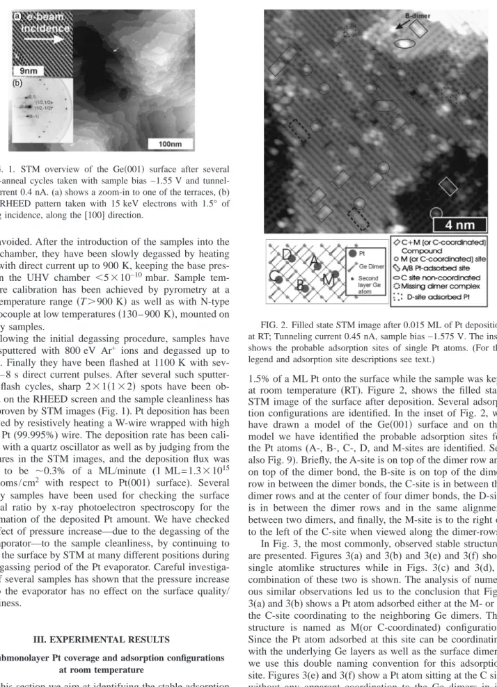
600 K. Finally they have been flashed at 1100 K with sev-eral 4 – 8 s direct current pulses. After sevsev-eral such sputter-degas-flash cycles, sharp 2⫻1共1⫻2兲 spots have been ob-served on the RHEED screen and the sample cleanliness has been proven by STM images(Fig. 1). Pt deposition has been achieved by resistively heating a W-wire wrapped with high purity Pt(99.995%) wire. The deposition rate has been cali-brated with a quartz oscillator as well as by judging from the structures in the STM images, and the deposition flux was found to be ⬃0.3% of a ML/minute (1 ML=1.3⫻1015
Pt—atoms/ cm2 with respect to Pt共001兲 surface). Several dummy samples have been used for checking the surface material ratio by x-ray photoelectron spectroscopy for the confirmation of the deposited Pt amount. We have checked the effect of pressure increase—due to the degassing of the Pt evaporator—to the sample cleanliness, by continuing to image the surface by STM at many different positions during the degassing period of the Pt evaporator. Careful investiga-tion of several samples has shown that the pressure increase due to the evaporator has no effect on the surface quality/ cleanliness.
III. EXPERIMENTAL RESULTS
A. Submonolayer Pt coverage and adsorption configurations at room temperature
In this section we aim at identifying the stable adsorption configurations of as-deposited Pt atoms. Following the re-peated cleaning cycles, we have deposited an equivalent of
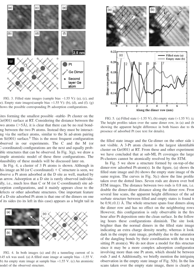
1.5% of a ML Pt onto the surface while the sample was kept at room temperature (RT). Figure 2, shows the filled state STM image of the surface after deposition. Several adsorp-tion configuraadsorp-tions are identified. In the inset of Fig. 2, we have drawn a model of the Ge共001兲 surface and on this model we have identified the probable adsorption sites for the Pt atoms(A-, B-, C-, D, and M-sites are identified. See also Fig. 9). Briefly, the A-site is on top of the dimer row and on top of the dimer bond, the B-site is on top of the dimer row in between the dimer bonds, the C-site is in between the dimer rows and at the center of four dimer bonds, the D-site is in between the dimer rows and in the same alignment between two dimers, and finally, the M-site is to the right or to the left of the C-site when viewed along the dimer-rows. In Fig. 3, the most commonly, observed stable structures are presented. Figures 3(a) and 3(b) and 3(e) and 3(f) show single atomlike structures while in Figs. 3(c) and 3(d), a combination of these two is shown. The analysis of numer-ous similar observations led us to the conclusion that Figs. 3(a) and 3(b) shows a Pt atom adsorbed either at the M- or at the C-site coordinating to the neighboring Ge dimers. This structure is named as M(or C-coordinated) configuration. Since the Pt atom adsorbed at this site can be coordinating with the underlying Ge layers as well as the surface dimers, we use this double naming convention for this adsorption site. Figures 3(e) and 3(f) show a Pt atom sitting at the C site without any apparent coordination to the Ge dimers in its vicinity. Figures 3(c) and 3(d) show the structure due to two Pt atoms placed in neighboring M(or C-coordinated) and C
FIG. 1. STM overview of the Ge共001兲 surface after several sputter-anneal cycles taken with sample bias −1.55 V and tunnel-ling current 0.4 nA.(a) shows a zoom-in to one of the terraces, (b) is the RHEED pattern taken with 15 keV electrons with 1.5° of gracing incidence, along the[100] direction.
FIG. 2. Filled state STM image after 0.015 ML of Pt deposition at RT; Tunneling current 0.45 nA, sample bias −1.575 V. The inset shows the probable adsorption sites of single Pt atoms.(For the legend and adsorption site descriptions see text.)
sites forming the smallest possible -stable- Pt cluster on the Ge共001兲 surface at RT. Considering the distance between the two atoms共⬎5Å兲, it is clear that there can be no real bond-ing between the two Pt atoms. Instead they must be interact-ing via the surface atoms, similar to the Si ad-atom pairinteract-ing on Si共001兲 surface.8This is the most frequent configuration
observed in our experiments. The C and the M (or C-coordinated) configurations are the next and equally prob-able structures that can be observed. In Fig. 3(g), we draw a simple atomistic model of these three configurations. The plausibility of these models will be discussed later on.
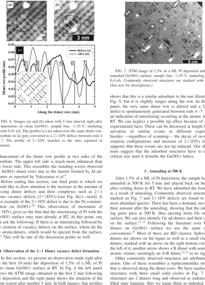
In Fig. 4, a cluster of 3 Pt atoms is shown. Although in this image an M(or C-coordinated)⫹ C structure is seen, we observe a Pt atom adsorbed at the D site as well, marked by an arrow. Adsorption at a D site is rarely observed individu-ally, i.e., much less than C or M(or C-coordinated) site ad-sorption configurations, and it mainly appears close to the defects or other adsorbate structures. One important feature of a D-site adsorbed Pt atom is that one of the dimers on one of its sides(to its left in this case) appears as a bright tail in
the filled state image and the Ge-dimer on the other side is not visible. A 3-Pt atom cluster is the largest identifiable cluster on Ge共001兲 at RT. From these and other experiments we have concluded that at sub-ML Pt coverages the larger Pt-clusters cannot be atomically resolved by the STM.
In Fig. 5 we show a structure formed by on-top-of-the-dimer-row adsorbed Pt-atom(s). In the figure, (a) shows the filled state image and(b) shows the empty state image of the same region. The curves in Fig. 5(c) show the line profiles taken over the dotted lines. Seven rods are drawn over both STM images. The distance between two rods is 0.8 nm, i.e., double the dimer-dimer distance along the dimer row. From several line scans, the apparent height difference of the ad-sorbate structure between filled and empty states is found to be 0.9共±0.1兲 Å. The whole structure spans four dimers along the dimer row and has no effect on the neighboring rows. However, this configuration is only observable in the first hour after Pt deposition onto the clean surface. In the follow-ing hours these configurations diminish. The site looks brighter than the normal dimers in the filled state image, indicating an extra charge density nearby, whereas it looks dark in the empty state image, probably due to the saturation of the dangling bonds by their coordination with the on top sitting Pt atom(s). We do not draw a model for this structure since it may be a more complex adsorption configuration involving more than one Pt atom, which should be between rods 3 and 4. Additionally, we briefly mention the intriguing observation in the empty state image of Fig. 5(b). In the line scans taken over the empty state image, there is clearly an
FIG. 3. Filled state images(sample bias −1.55 V): (a), (c), and
(e). Empty state images(sample bias +1.55 V): (b), (d), and (f). (g)
shows the possible corresponding Pt adsorption configurations.
FIG. 4. In both images (a) and (b) a tunneling current of is 0.45 nA was used.(a) A filled state image at sample bias −1.55 V.
(b) An empty state image at sample bias +1.55 V. (c) An atomistic
model of the observed structure.
FIG. 5.(a) Filled state共−1.55 V兲, (b) empty state 共+1.55 V兲. (c) The height profiles taken over the same dimer row, in(a) and (b)
showing the apparent height difference in both biases due to the presence of adsorbed Pt(see text for details).
enhancement of the dimer row profile at two sides of the adsorbate. The upper left side is much more enhanced than the lower side. This resembles the standing waves observed on Si共001兲 dimer rows due to the barrier formed by Al-ad-dimers as reported by Yokoyama et al.9
Before ending this section, one final point to which we would like to draw attention is the increase in the amount of missing dimer defects and their complexes such as 2 + 1 dimer vacancy defects(2⫹1DVs) [see Fig. 6(c)—inset]. A nice example of the 2⫹1DV defect is due to the Ni contami-nation on Si共001兲.10 This observation of increment of
2⫹1DVs gives us the hint that the intermixing of Pt with the Ge共001兲 surface may start already at RT. At this point, one can ask the following: If there is an intermixing followed by the creation of vacancy defects on the surface, where do the Ge atoms/dimers, which would be ejected from the surface, go? This will be one of the discussion points as well.
B. Observation of the 2 + 1 Dimer vacancy defect formation
In this section, we present an observation made right after (in the first 10 min) the deposition of 1.5% of a ML of Pt onto clean Ge共001兲 surface at RT. In Fig. 6 the left panel shows the STM image obtained in the first 5 min following the deposition and the right panel shows the situation of the same region after another 5 min. In both images, line profiles are drawn over the same dimer row. In the left panel, the dimer row has an on-top adsorbed structure. The line scan
shows that this is a similar adsorbate to the one illustrated in Fig. 5, but it is slightly longer along the row. In the right panel, the very same dimer row is altered and a 2⫹1DV defect is spontaneously generated between rods 4 – 7. This is an indication of intermixing occurring at the atomic level, at RT. We can neglect a possible tip effect because of several experimental facts. These can be discussed at length but ob-servation of similar events at different experiments besides —regardless of scanning— the decay of on-top ad-sorption configurations and increase of 2⫹1DVs in time, supports that these events are not tip induced. Our observa-tions suggest that the adsorbed structures have to reach a critical size until it disturbs the Ge共001兲 lattice.
C. Annealing at 500 K
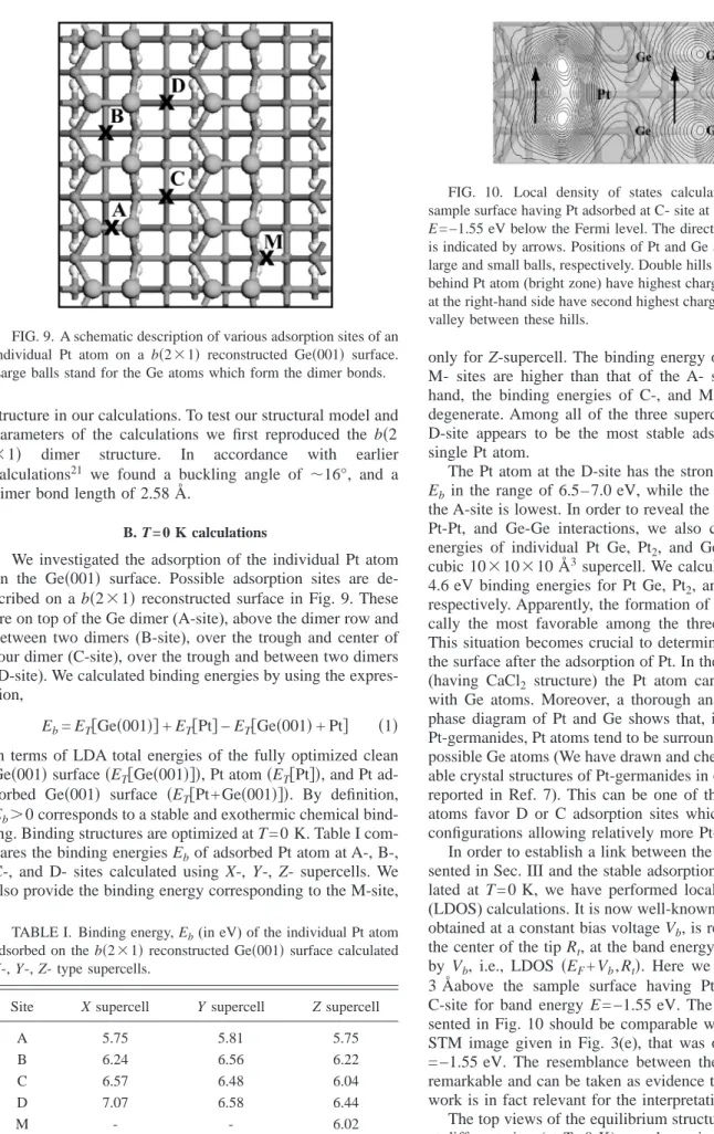
After 1.5% of a ML of Pt deposition, the sample has been annealed at 500 K for 5 min and placed back on the STM after cooling down to RT. We have identified the formations as a result of annealing. Commonly observed structures are marked on Fig. 7 and 2⫹1DV defects are found to be the most abundant species. There has been a dramatic increase in their amount after the annealing, showing that the intermix-ing gains pace at 500 K, thus ejectintermix-ing more Ge onto the surface. We can also identify Ge ad-dimers and their clusters on the surface.11–13 Following the literature over Ge
ad-dimers on Ge共001兲 surface we use the same naming conventions.27 Most of these are BD clusters. Individual B
dimers are shown on the figure as well as a small cluster of dimers, marked with an arrow on the right bottom corner. To the left of it, another arrow shows a B dimer with some other atomic cluster, seemingly an A/B dimer,11,12to its right.
Other commonly observed structures are attributed to Pt atoms. One of these resembles a replacementlike structure, that is observed along the dimer rows. We have marked these structures with three small solid circles in Fig. 7. These structures are 2 dimers long and observed as indents in the filled state imaging, thus we name them as indented dimers (IDs). Their depth is less than that of single dimer vacancy (DV) defects, and their topography looks different than the
FIG. 6. Images(a) and (b) taken with 5 min interval right after Pt deposition on clean Ge共001兲; sample bias −1.55 V, tunneling current 0.45 nA. The profiles(c) are taken over the same dimer row. Adsorbate in(a) gets converted to a 2+1DV defect, between rods 4 to 7. The profile of 2 + 1DV matches to the ones reported in literature.
FIG. 7. STM image of 1.5% of a ML Pt deposited and 500 K annealed Ge共001兲 surface; sample bias −1.55 V, tunneling current 0.4 nA. Commonly observed structures are marked with shapes.
single DV defects; so we rule out the possibility that they may be missing dimers. However, further modeling without considering all the possible models and checking them with theoretical predictions would merely be a speculation. Two more configurations are shown in Fig. 7. These structures, although resemble some of the structures discussed in Sec. III A, cannot be mapped onto those in a one to one manner. The single dotlike structures sitting in between the dimer rows are marked with small ellipses, and they are probably due to Pt atoms adsorbed at M(or C- coordinated) sites. The final most common structures are marked by larger ellipses in Fig. 7. These are the doubling of the structures marked by small ellipses. This may be a more stable state of the struc-ture given in Figs. 3(c) and 3(d), which might have become accessible due to the increased temperature, and the two ad-sorbates create a more stable configuration due to a substrate mediated(concerted) interaction of Pt atoms.
D. Annealing at 900 K
Following the observations above, the sample has been annealed at 900 K for 5 min. The resulting surface(Fig. 8) has 2⫹1DV defects as the most common structure and IDs are in abundance. The only adsorbate is observed at D sites, but rarely(marked with circles in Fig. 8). IDs have variation among themselves. The double structure marked by a dashed ellipse on the upper side has two of these with a regular dimer in between, and IDs are more to the right(ID-R). The one on the lower left side of the figure, marked with a solid ellipse, has a more to-the-left position(ID-L). Moreover the one to its right (central bottom part of the figure), again marked with a solid ellipse, has a more central position when viewed along the dimer row (ID-C). The alteration of the buckling registries of the dimer rows on both sides of these structures(along the rows) is to be mentioned as well.
Further annealing at higher temperatures共T⬎900 K兲 re-sults only in 2⫹1DV defects and IDs as the remaining for-mations. As a function of the Pt coverage, the terraces of the Ge共001兲 surface get completely altered and even nanowires form as we have recently reported.7
IV. THEORETICAL METHOD
The first-principles total energy and electronic structure calculations have been performed using the pseudopotential
k-points in Brillouin zone sampling has been determined
ac-cording to results of an extensive convergence tests. To this end we calculated total energies of various relaxed structures with different number of k-points; among these k-points we selected the smallest number of k-points, where the differ-ence in the total energy between two consecutive sampling set is in the range of approximately 1 meV. We used 8 k-points for共2⫻2兲-supercell; 8 k-points for 共4⫻1兲 super-cell; and 4 k-points for共4⫻2兲 supercell. The atomic struc-tures are optimized by using conjugate gradient method in the zero-temperature calculations. Furthermore, in order to simulate the diffusion of the adsorbed Pt atom, we also car-ried out finite temperature, ab initio molecular dynamics cal-culations at 1000 K by using Nosé15 thermostat.
V. THEORETICAL RESULTS A. Ge„001…, 2Ã1 surface
The Ge共001兲 surface was modeled by a five-layer slab with a vacuum region of 13 Å. Bottom Ge-layer atoms were saturated by H atoms. While the positions of bottom Ge and H atoms have been kept fixed, the Ge atoms in the top four layers have been relaxed in the course of structure optimiza-tion. In order to study Pt adsorption, three different types of supercell structures (i.e., X-, Y-, and Z- supercells) were used. It is well established that Ge共001兲 surface reconstructs with dimer bond formation. The symmetric versus asymmet-ric nature of the dimer bond has been an important issue for both theoretical and experimental investigations. Many theoretical16–18 and experimental19 works have favored the asymmetric dimers. Besides, in addition to the buckled b共2 ⫻1兲, higher order reconstructions of Ge共001兲 surface, such as c共4⫻2兲 or p共2⫻2兲 have been observed.20–22 These
higher-order reconstructions are close in energy20 and occur
depending on different arrangements of asymmetric dimer bonds. Nevertheless, a commonly accepted picture of the re-constructed Ge共001兲 surface consists of an asymmetric dimer ordering in a(2x1) structure at room temperature (RT), while the surface reconstructs according to a c共4⫻2兲 arrangement at low temperature. In addition, Needels et al.17,18found the
c共4⫻2兲 and p共2⫻2兲 reconstructions are almost degenerate
and their energy is approximately 0.07 eV per dimer lower than that of the b共2⫻1兲 structure. They also suggested the existence of a phase transition at 380± 100 K, between the ordered c共4⫻2兲 or p共2⫻2兲 state and the disordered b共2 ⫻1兲 state.18 We used b共2⫻1兲 buckled dimerized surface
annealed Ge共001兲 surface; sample bias −1.55 V, tunneling current 0.4 nA. Commonly observed structures are marked with shapes.
structure in our calculations. To test our structural model and parameters of the calculations we first reproduced the b共2 ⫻1兲 dimer structure. In accordance with earlier calculations21 we found a buckling angle of ⬃16°, and a
dimer bond length of 2.58 Å.
B. T = 0 K calculations
We investigated the adsorption of the individual Pt atom on the Ge共001兲 surface. Possible adsorption sites are de-scribed on a b共2⫻1兲 reconstructed surface in Fig. 9. These are on top of the Ge dimer(A-site), above the dimer row and between two dimers (B-site), over the trough and center of four dimer(C-site), over the trough and between two dimers (D-site). We calculated binding energies by using the expres-sion,
Eb= ET关Ge共001兲兴 + ET关Pt兴 − ET关Ge共001兲 + Pt兴 共1兲
in terms of LDA total energies of the fully optimized clean Ge共001兲 surface 共ET关Ge共001兲兴兲, Pt atom 共ET关Pt兴兲, and Pt
ad-sorbed Ge共001兲 surface 共ET关Pt+Ge共001兲兴兲. By definition, Eb⬎0 corresponds to a stable and exothermic chemical
bind-ing. Binding structures are optimized at T = 0 K. Table I com-pares the binding energies Ebof adsorbed Pt atom at A-, B-,
C-, and D- sites calculated using X-, Y-, Z- supercells. We also provide the binding energy corresponding to the M-site,
only for Z-supercell. The binding energy of B-, C-, D-, and M- sites are higher than that of the A- site. On the other hand, the binding energies of C-, and M- sites are almost degenerate. Among all of the three supercell structures, the D-site appears to be the most stable adsorption site for a single Pt atom.
The Pt atom at the D-site has the strongest bonding with
Eb in the range of 6.5– 7.0 eV, while the binding energy at the A-site is lowest. In order to reveal the strength of Pt-Ge, Pt-Pt, and Ge-Ge interactions, we also calculated binding energies of individual Pt Ge, Pt2, and Ge2 molecules in a
cubic 10⫻10⫻10 Å3supercell. We calculated 7.3, 4.9, and
4.6 eV binding energies for Pt Ge, Pt2, and Ge2 molecules,
respectively. Apparently, the formation of Pt-Ge is energeti-cally the most favorable among the three types of bonds. This situation becomes crucial to determine the character of the surface after the adsorption of Pt. In the case of Pt Ge2,23
(having CaCl2 structure) the Pt atom can make six bonds
with Ge atoms. Moreover, a thorough analysis of the bulk phase diagram of Pt and Ge shows that, in all the reported Pt-germanides, Pt atoms tend to be surrounded by as many as possible Ge atoms(We have drawn and checked all the avail-able crystal structures of Pt-germanides in our previous work reported in Ref. 7). This can be one of the reasons why Pt atoms favor D or C adsorption sites which provide atomic configurations allowing relatively more Pt-Ge bonds.
In order to establish a link between the STM images pre-sented in Sec. III and the stable adsorption sites of Pt calcu-lated at T = 0 K, we have performed local density of states (LDOS) calculations. It is now well-known that STM images obtained at a constant bias voltage Vb, is related to LDOS at the center of the tip Rt, at the band energy of the sample set
by Vb, i.e., LDOS 共EF+ Vb, Rt兲. Here we calculated LDOS
3 Åabove the sample surface having Pt adsorbed at the C-site for band energy E = −1.55 eV. The contour plot pre-sented in Fig. 10 should be comparable with the filled state STM image given in Fig. 3(e), that was obtained using Vb
= −1.55 eV. The resemblance between these two figures is remarkable and can be taken as evidence that the theoretical work is in fact relevant for the interpretation of experiment. The top views of the equilibrium structure of Pt, adsorbed at different sites(at T=0 K), are shown in Figs. 11(a), 12(a),
FIG. 9. A schematic description of various adsorption sites of an individual Pt atom on a b共2⫻1兲 reconstructed Ge共001兲 surface. Large balls stand for the Ge atoms which form the dimer bonds.
TABLE I. Binding energy, Eb(in eV) of the individual Pt atom
adsorbed on the b共2⫻1兲 reconstructed Ge共001兲 surface calculated
X-, Y-, Z- type supercells.
Site X supercell Y supercell Z supercell
A 5.75 5.81 5.75
B 6.24 6.56 6.22
C 6.57 6.48 6.04
D 7.07 6.58 6.44
M - - 6.02
FIG. 10. Local density of states calculated 3 Å above the sample surface having Pt adsorbed at C- site at T = 0 K due to states
E = −1.55 eV below the Fermi level. The direction of dimmer rows
is indicated by arrows. Positions of Pt and Ge atoms are shown by large and small balls, respectively. Double hills at the left-hand side behind Pt atom(bright zone) have highest charge density. Two hills at the right-hand side have second highest charge density. There is a valley between these hills.
13(a), and 14(a). At the A- site, the adsorbed Pt atom forms two bonds with Ge atoms at both sides of the Ge-Ge dimer bond. The B-site, which is energetically more favorable than the A-site, offers four bonds to the Pt atom adsorbed between two adjacent dimer bonds, as seen in Fig. 11(b). At the C-site, Pt is adsorbed and coordinated with neighboring two Ge atoms. An interesting change in the structure of Ge共001兲-共2⫻1兲 is observed when Pt is adsorbed at the D-site. As shown in Fig. 14(a), the adsorbed Pt atom shifts slightly to the right and pulls one of the Ge atoms by break-ing the left-hand side dimer. It forms two new Pt-Ge bonds this way. The energy associated with the breaking of one dimer bond is compensated by forming two additional Pt-Ge bonds in a concerted process.
To analyze the effect of high coverage of Pt we also per-formed calculations to obtain the binding structure and
bind-ing energy of two coadsorbed Pt atoms. We have particularly examined the Pt atoms adsorbed at the adjacent sites, such as A-A, A-B, A-C, B-D, C-C, D-D, and D-C. In accordance with the above analysis which compares the strengths of dif-ferent types of bonds(such as Pt-Pt, Pt-Ge, Ge-Ge), we did not observe a tendency for clustering of adsorbed Pt atoms. Because of its relevance to the experimental data, we also examined coadsorption at M- and C- sites at the adjacent troughs. While the individual adsorption of Pt at C-, and M- sites has binding energies of 6.04 and 6.02 eV, respec-tively, the coadsorption resulted in a total energy of 12.26 eV. Thus such a concerted bond through the Ge lattice is favored by⬃0.2 eV.
C. Ab initio finite temperature calculations
In order to analyze the motion of adsorbed Pt atoms onto Ge共001兲 and hence to reveal atomic scale mechanisms lead-ing to orderlead-ing and other structural modifications at finite temperature, we performed ab initio molecular dynamics cal-culations at 1000° K. A relatively high temperature is chosen to enhance the statistics. Initially, adsorbed Pt atoms were placed on A-, B-, C-, and D- sites as in Fig. 9, at heights different from the positions optimized at T = 0 ° K. The new
FIG. 11. Time evolution of the Pt atom initially adsorbed at the
A-site:(a) The top view of the atomic structure at T=0°K. The top
view(b), and the side view (c) of the atomic structure evolved for 1100 time steps at T = 1000° K. Each time step lasts 1 fs= 10−15s.
(d) The variation of the height of adsorbed Pt atom with time at
1000 K. The zero of the height of the Pt atom is set at its optimized structure at T = 0 ° K. Pt, surface Ge, subsurface Ge, and saturating H atoms are described by large-dark, medium-gray, small-gray, and small-white balls, respectively. Dimer rows are running in the(111) direction.
FIG. 12. Time evolution of the Pt atom initially adsorbed at the B-site.
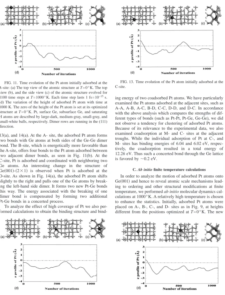
FIG. 13. Time evolution of the Pt atom initially adsorbed at the C-site.
FIG. 14. Time evolution of the Pt atom initially adsorbed at the D- site.
positions of Pt atoms after 1100 time steps (iterations) are presented in Figs. 11–13, 14(b), and 14(c). We observe a trend which is common to all four initial adsorption sites. The Pt atoms tend to dive below the surface dimer. At the A-site, the adsorbed atom leaves its initial position and moves downward by ⬃2.5 Å, by causing a significant change on the surface structure. The Pt atom initially ad-sorbed at the B-site, moves downward by ⬃3 Å and goes below the second Ge layer. Since C- and D- sites are in the trough, Pt atoms adsorbed at these sites have relatively small downward motion. However, for all four adsorption sites a massive change of surface structure follows the motion of Pt. The driving force for the movement of Pt atoms toward the subsurface is to find interstitial sites which accommodate more Pt-Ge bonds with neighboring Ge atoms. In summary, the ab initio finite temperature MD results indicate that ad-sorbed Pt atoms escape from the surface and fall below the surface Ge atoms.
VI. DISCUSSION
A. Stable Pt adsorption configurations at room temperature on Ge„001… surface
The total energy calculations support the domination of the trough site adsorption of Pt atoms(C and D). Besides, they predict an instability of the on top sites(A and B) such that the Pt atoms that would normally occupy these positions instead have a driving force to go to the higher coordination sites. The lack of dominance of D configurations but instead the high number of M(or C-coordinated) and C configura-tions can be explained as follows: Although the D-site is shown to be more stable than the C-site, this binding requires the breaking up of neighboring Ge-dimers even at 0 K(Fig. 14), while the substrate is frozen and dimers are in the b共2 ⫻1兲 state. At room temperature, the dimers are flip-flopping between two buckled states.24A Pt adsorption to the D site
releases a considerable amount of energy(up to 6.5 eV). We speculate that the released energy may cause a chain reaction that may lead to the breaking of many surface Ge bonds, destabilizing the Pt atom and eliminating the chance of existence of this configuration. As a result, C site adsorption—which does not lead to a bond breaking— be-comes the highest probable configuration. The observation of D-site adsorption near the defects or other Pt adsorbate sites may support this argumentation, because defects and adsor-bates generally pin the flip-flopping of the dimers25and may
dampen the transfer of the energy released due to the break-ing of the bonds on the surface.
We note that most of the observed C-site configurations are named as M (or C-coordinated). When the calculated configuration for the C-site at 0 K is carefully analyzed, a slight relaxation toward the M site is noticed. Moreover, C and M configurations are energetically almost degenerate (Table I). At RT, the pulling of the neighboring Ge-dimer toward the Pt atom can be enhanced by generating a suitable C site for an additional Pt atom on the neighboring dimer row’s C-site. This would explain the abundance of C + M(or C-coordinated) configurations at RT (see Figs. 2 and 3). The 200 meV energy gain due to the concerted bonding of two Pt
atoms at neighboring trough sites is an additional enhance-ment factor for this configuration. Conclusively, we can state that C and C + M(or C- coordinated) sites are the most stable Pt-adsorption configurations on Ge共001兲 surface at RT. The absence of Pt dimers, but instead the formation of concerted bonding between two Pt atoms through the surface is both observed in STM images and confirmed by calculations. Consequently, our models given in Figs. 3 and 4 are plau-sible with a slight modification to the D-configuration in Fig. 4(c), such that the Ge-dimer to the left of the D site is prob-ably broken.
B. Meta-stable adsorption sites and spontaneous generation of 2 + 1 dimer vacancy defects at room temperature
A- or B-site adsorption is shown to be less probable due to lesser stability in comparison to adsorption at C and D sites. The calculations suggest that at elevated temperatures there is a driving force for the Pt atoms adsorbed at these sites to dive under the surface(Figs. 11 and 12). Our experi-ments comply with these results, such that the amount of on-top configurations decay in time at RT. Since we do not observe a significant increase of D or C configurations in time, and our decay-observations like in Fig. 6 indicate a certain dependence of the decay event on the adsorbate size, we conclude that the diffusivity of Pt atoms should be higher along the dimer rows than perpendicular to the dimer rows. Thus, another conclusive result is that the intermixing of Pt with Ge共001兲 surface starts at RT. The starting position of intermixing is identified to be A or B adsorption sites pro-vided that the local adsorbate density is above a critical value. Judging from the STM images, this critical value is Ⰷ3 on top adsorbed Pt atoms per 2 Ge-dimers, along the dimer row(see Figs. 5 and 6). This is supported by the cal-culations as well: Fewer than 3 on-top-of-the-dimer-row ad-sorbed Pt atoms do not change their surroundings at 0 K. Further calculations are essential using bigger supercells, re-quiring higher computing power.
C. Stable adsorption configurations at elevated temperatures
Annealing experiments at 500 K show that M(or C- coor-dinated) and a few D configurations survive. The C+M (or C- coordinated) configurations are converted to M+M con-figurations. The overall reduction of the amount of C and D configurations and the increase of 2⫹1DV defects hint at the easing of across the dimer row diffusion, followed by an in-diffusion of Pt atoms, ultimately ending at subsurface po-sitions. The 900 K experiments indicate, the D- site as the most stable adsorption configuration (see Fig. 8). The 1000 K calculations show that Pt atoms do not diffuse deeper into the bulk but rather get pinned in the near surface region, some of which right under the dimers. Besides, in 900 K experiments we observed indented-dimer(ID) struc-tures. Looking at the high temperature models, one can pre-dict that these actually are dimers, but right under them a Pt atom is coordinating with their dimer bonds, changing their apparent height along with their buckling. Depending on the position of the subsurface Pt, the observed asymmetries can occur(i.e., ID-C, ID-L, ID-R). The in-diffusion of Pt atoms
place during the progressions from C and D sites, at elevated temperatures. Therefore, we suggest that a Pt atom progress-ing from the A-site can generate the 2 + 1DV defects in com-bination with another Pt atom either progressing from the A-or B- site, but ID structures should be a result of progression from B-sites(see Figs. 11 and 12). We eliminate a similar scenario due to progression from C- and D- sites because their height progression clearly shows that a Pt atom origi-nating from one of these sites should be more or less visible to the STM as they do not sink into the surface(see Figs. 12 and 13).
D. Intermixing and Ge ejection onto the surface
The 1000 K calculations show breaking of the bonds of the Ge surface lattice in the vicinity of Pt atoms. Conse-quently, one expects that the broken-off Ge atoms should generate Ge ad-dimers on the surface. The diffusion barrier for a Ge monomer on Ge共001兲 surface is about 0.6 eV, meaning that such an atom can make 400 hops per second, on the surface at RT. However, the spontaneous generation of 2 + 1DV defects are quite rare at RT. The monomer density on the surface is required to be high enough before they can form dimers. We have observed a few B ad-dimers on the surface in the RT experiments. Also in data like those shown in Fig. 6 no ad-dimer is observable nearby the generated 2 + 1DVs. Considering the diffusion barrier for the Ge-dimers on Ge共001兲 surface, which is about 0.8 eV, this structure can visit far less surface positions than a monomer (making
VII. CONCLUSIONS
In this study we have identified the stable adsorption sites/ configurations of Pt atoms on Ge共001兲 surface using STM measurements and density functional theory calculations. Our calculations predict that, a concerted bonding of two Pt atoms through the Ge lattice is more favorable on the Ge共001兲 surface than a direct Pt-Pt bond. This is confirmed with STM observations. Additionally, we have found meta-stable adsorption configurations at RT, some of which decay resulting in the spontaneous generation of 2 + 1 dimer va-cancy defects during the in-diffusion of Pt atoms at RT. Along with the adsorption configurations, we have studied the high temperature behavior of Pt atoms on the surface and identified several on-top adsorption configurations. Several subsurface configurations of Pt atoms are also identified at high temperatures, through finite temperature ab initio mo-lecular dynamic calculations, which help understand the lo-cal reconstructions occurring at elevated temperatures. Fur-thermore, we have discussed the ejection of Ge atoms onto the Ge共001兲 surface due to the intermixing of Pt with the substrate at various temperatures, resulting in Ge ad-atoms and ad-dimers on the surface.
ACKNOWLEDGMENTS
This work is financially supported by the Stichting Fun-damental Onderzoek der Materie(FOM) of the Netherlands.
*Electronic mail: [email protected]
1G. Binnig, H. Rohrer, C. Gerber, and E. Weibel, Phys. Rev. Lett.
49, 57(1982).
2L. H. Chan and E. I. Altman, Phys. Rev. B 66, 155339(2002). 3K. Hattori, Y. Takahashi, T. Iimori, and F. Komori, Surf. Sci.
357–358, 361(1995).
4M. G. Grimaldi, L. Wielunski, M.-A. Nicolet, and K. Tu, Thin
Solid Films 81, 207(1981).
5Y. F. Hsieh and L. J. Chen, J. Appl. Phys. 63, 1177(1987). 6J. J. Rosenberg, IEEE Trans. Electron Devices 30, 1602(1983). 7O. Gurlu, O. A. O. Adam, H. J. W. Zandvliet, and B. Poelsema,
Appl. Phys. Lett. 83, 4610(2003).
8R. A. Wolkow, Phys. Rev. Lett. 74, 4448(1995).
9T. Yokoyama, M. Okamoto, and K. Takayanagi, Phys. Rev. Lett.
81, 3423(1998).
10V. A. Ukraintsev and J. T. Yates, Surf. Sci. 346, 31(1996). 11E. Zoethout, H. J. W. Zandvliet, and B. Poelsema, J. Vac. Sci.
Technol. A 19, 1868(2001).
12T. M. Galea, C. Ordas, E. Zoethout, H. J. W. Zandvliet, and B.
Poelsema, Phys. Rev. B 62, 7206(2000).
13H. J. W. Zandvliet, T. M. Galea, E. Zoethout, and B. Poelsema,
Phys. Rev. Lett. 84, 1523(2000).
14H. J. Monkhorst and J. D. Pack, Phys. Rev. B 13, 5188(1976). 15S. Nosé, J. Chem. Phys. 81, 511(1984).
16P. Krüger, A. Mazur, J. Pollman, and G. Wolfgarten, Phys. Rev.
Lett. 57, 1468(1986).
17M. Needels, M. C. Payne, and J. D. Joannopoulos, Phys. Rev.
18M. Needels, M. C. Payne, and J. D. Joannopoulos, Phys. Rev. B
38, 5543(1988).
19J. A. Kubby, J. E. Griffith, R. S. Becker, and J. S. Vickers, Phys.
Rev. Lett. 36, 6079(1987).
20J. Ihm, D. H. Lee, J. D. Joannopoulus, and J. J. Xiong, Phys. Rev.
Lett. 51, 1872(1983).
21L. Spiess, A. J. Freeman, and P. Soukiassian, Phys. Rev. B 50,
2249(1994).
22H. J. W. Zandvliet, Phys. Rep. 388, 1(2003).
23T. B. Massalski and H. Okamoto, Binary Alloy Phase Diagrams,
Vol. 3(ASM International, Materials Park, OH, 1990).
24T. Sato,M. Iwatsuki, and H. Tochihara, J. Electron Microsc. 48, 1
(1999).
25S. J. Murray, M. Mian, and F. M. L. R. McGrath, Surf. Sci.
307–309, 741(1994).
26E. van Vroonhoven, H. J. W. Zandvliet, and B. Poelsema, Phys.
Rev. Lett. 91, 116102(2003).
27An A dimer is an ad-dimer attached on top of the dimer row in
between the surface diners and lies parallel to them. B dimer is again an as-dimer row in between the surface dimers but lies perpendicular to them. C and D dimers lie in between the dimer rows and they are centered among 4 surface dimers. C lies par-allel to the dimer rows and D lies perpendicular to them.