AFM/STM
a dissertation submitted to
the department of physics
and the institute of engineering and science
of bilkent university
in partial fulfillment of the requirements
for the degree of
doctor of philosophy
By
MEHRDAD ATABAK
September, 2007
Prof. Dr. Ahmet Oral (Supervisor)
I certify that I have read this thesis and that in my opinion it is fully adequate, in scope and in quality, as a dissertation for the degree of doctor of philosophy.
Prof. Dr. S¸efik S¨uzer
I certify that I have read this thesis and that in my opinion it is fully adequate, in scope and in quality, as a dissertation for the degree of doctor of philosophy.
Assoc. Prof. Dr. O˘guz G¨ulseren
Assist. Prof. Dr. Hakan ¨Ozg¨ur ¨Ozer
I certify that I have read this thesis and that in my opinion it is fully adequate, in scope and in quality, as a dissertation for the degree of doctor of philosophy.
Assist. Prof. Dr. Ceyhun Bulutay
Approved for the Institute of Engineering and Science:
Prof. Dr. Mehmet B. Baray Director of the Institute
DYNAMIC MODE USING COMBINED AFM/STM
MEHRDAD ATABAKPhD in Physics
Supervisor: Prof. Dr. Ahmet Oral September, 2007
In this Ph.D. work, we constructed a fiber optic interferometer based non-contact Atomic Force Microscope (nc-AFM) combined with Scanning Tunneling Micro-scope(STM) to study lateral force interactions on Si(111)-(77) surface. The in-terferometer has been built in such a way that its sensitivity surpasses that of the earlier versions used in normal force measurements. The improvement in the resolution of the interferometer has allowed us to use sub-Angstrom oscillation amplitudes to obtain quantitative lateral force measurements. We have observed single and double atomic steps on Si(111)-(77) surface in topography and lat-eral stiffness images. This information allowed us to measure the latlat-eral forces directly and quantitatively. We have also carried out lateral force-distance spec-troscopy experiments, in which we simultaneously measured the force gradient and tunneling current, as the sample is approached towards the tip. The lateral force?distance curves exhibit a sharp increase of the force gradient, just after the tunnel current starts to increase, while the sample is approaching to the tip. We observed only positive force gradients.
In separate experiments, we imaged the Cu-TBPP molecules deposited on Cu(100) surface in normal and torsional mode in dynamic force microscope us-ing STM feedback, with a homemade tungsten cantilever. Our experiments have shown the possibility of manipulating molecules on surface using a vibrating can-tilever. However the forces involved in these experiments are not quantitatively measured due to limitations of the method.
Keywords: Scanning Probe Microscopy, Scanning Tunnelling Microscopy,
noncon-tact Atomic Force Microscope, Cantilever, Lateral nonconnoncon-tact Force Microscopy, Fiber Interferometer.
YATAY KUVVETLERI˙IN D˙INAM˙IK K˙IPTE ATOM˙IK
KUVVET M˙IKROSKOBU/TARAMALI T ¨
UNELLEME
M˙IKROSKOBU ˙ILE ˙INCELENMES˙I
MEHRDAD ATABAKFizik, Doktora
Tez Y¨oneticisi: Prof. Dr. Ahmet Oral Eylul, 2007
Bu doktora ¸calı¸smasında u¸c ile y¨uzey arası yatay kuvvetleri k¨u¸c¨uk genlikle titre¸stirerek ¨ol¸cebilen fiber optik interefrometre kullanan Y¨uzeye De˘gmeden Atomik Kuvvet Mikroskobu (YD-AKM)/Taramalı T¨unelleme Mikroskobu(TTM) imal edilerek, bununla Si(111)-(7×7) y¨uzeyinde yatay kuvvetler incelenmi¸stir. Geli¸stirilen interferometre daha ¨once dik kuvvet ¨ol¸cmede kullanılana g¨ore ¸cok daha hassastır. Elde edilen bu y¨uksek ¨ol¸c¨um hassasiyeti nedeniyle yay Angstrom alti genliklerle titre¸stirilerek yatay u¸c-y¨uzey etkile¸simleri nicem-sel olarak ¨ol¸c¨ulebilmi¸stir. Si(111)-(7×7) y¨uzey topografi ve yatay esneklikte g¨or¨unt¨ulerinde tek ve ¸cift atomik basamakları nicemsel olarak g¨ozlenmi¸stir. U¸c y¨uzeye yakla¸stırılarak u¸c-y¨uzey yatay yay etkile¸sim yay sabiti ve t¨unel akımı uzaklı˘gın fonksiyonu olarak ¨ol¸c¨ulm¨u¸st¨ur. Yatay yay sabitinde tunel akımından sonra hızlı bir y¨ukselme g¨ozlenmi¸stir. Deneylerimizde yalnızca pozitif yatay yay sabiti g¨ozlenmi¸stir.
Di˘ger deneylerimizde ise yatay kuvvetleri yayın b¨uk¨ulmesini ¨ol¸cerek ¸calı¸san bir dinamik kuvvet mikroskobu ve elde yapılan bir tungsten yay kullanılarak Cu-TBPP molek¨ullerininin Cu(100) y¨uzeyi ile olan etkile¸simleri incelenmi¸stir. Deney-lerimiz Cu-TBPP molek¨ullerininin titreıen yay kulllanılarak Cu(100) y¨uzeyinde hareket ettirilebilece˘gini g¨ostermi¸stir. Fakat Basel ¨Universitesindeki bu d¨uzenek ile bu kuvvetleri nicemlendirmek m¨umk¨un olamamı¸stır.
Anahtar s¨ozc¨ukler : Taramalı U¸c Mikroskobu, Taramalı T¨unelleme Mikroskobu,
y¨uzeye de˘gmeden Atomik Kuvvet Mikroskobu, yay, yatay y¨uzeye de˘gmeden Atomik Kuvvet Mikroskobu, fiber intereferometre.
It is my pleasure to express my deepest gratitude to my advisor Prof. Dr. Ahmet Oral for his guidance, moral support, friendship and assistance during my Ph.D. thesis. I am indebted for his efforts and enthusiasm. I also express my deep appreciation to Dr. ¨Ozg¨ur ¨Ozer who made me familiar with Ultra High Vacuum techniques and Atomic Force Microscopy while I was his assistant during his Ph.D. work.
I would like to thank the members of my Ph.D. dissertation committee for reading the manuscript and commenting on the thesis.
I would like to thank our group members M¨unir Dede, Dr. ¨Ozhan ¨Unverdi, Sevil ¨Ozer, and Aslı Elidemir, Dr. Rizwan Akram, for creating a fruitful, enjoy-able, and unique working environment. I would like to acknowledge NanoMagnet-ics Instrument Ltd., former and current company members, Muharram, G¨oksel,
¨
Ozge, ¨Ozg¨ur, Volkan, Koray, for close collaboration and assistance whenever I needed.
I also would like to acknowledge ESF Nanotribo Program and Prof. Ernst Meyer to give me the opportunity to perform series of experiment in University of Basel, Switzerlands.
I would like to express my spacial thanks to A¸skin Kocaba¸s for his enthusiasm to create scientific discussions, and supplying me an extra pair of hands in my difficult times during experiment preparation. I also thank to Se¸ckin for helping my to model the Fabry-Perot interferometer. I would like to thank Dr. Aykutlu Dˆanˆa for his valuable comments on my experiments. I appreciate the help of the physicist Murat G¨ure and the technician Erg¨un Karaman.
I am indebted to my family for their continuous support, care, and encour-agement.
And finally, I thank my dearest Mehrnaz, as she means so much for me. I would like to devote this work to her and my family.
1 Introduction 1
1.1 Overview . . . 1
1.2 The Aim of the Dissertation . . . 3
2 Background 5 2.1 Scanning Tunnelling Microscopy . . . 6
2.1.1 STM Imaging . . . 8
2.1.2 Theory of STM . . . 10
2.1.3 Scanning Tunnelling Spectroscopy . . . 12
2.1.4 STM on Semiconductors . . . 14
2.2 Atomic Force Microscopy . . . 15
2.2.1 Nature of contributing forces in AFMs . . . 21
2.2.2 Sensitivity of AFMs . . . 22
2.3 Pathway from atomic resolution imaging to single atom manipulation 26 2.3.1 Atomic resolution imaging using STM . . . 26
2.3.2 Atomic resolution imaging in contact mode AFM . . . 29
2.3.3 Atomic resolution imaging in non-contact mode AFM . . . 31
2.3.4 Force Measurement by STM . . . 34
2.3.5 Force Measurement by AFM . . . 36
2.3.6 Molecule and atom manipulation . . . 38
2.4 Lateral force microscopy at the atomic scale . . . 40
3 Instrumentation and Noise Analysis 46 3.1 The ultra-high vacuum (UHV) system . . . 47
3.2 Cantilever/Sample Transfer and electron beam heater . . . 47
3.3 Construction of combined lateral non-contact AFM and STM . . 51
3.3.1 The Sample Slider . . . 53
3.3.2 Scanning Mechanism . . . 53
3.3.3 I-V Converter . . . 57
3.3.4 The Fiber Sliders . . . 58
3.3.5 The Cantilever Mount . . . 60
3.3.6 Cantilever preparation . . . 61
3.3.7 Sample and Cantilever Holder . . . 63
3.3.8 Interferometry based force sensing technique . . . 64
3.3.9 Fiber Preparation for introducing into the UHV chamber . 68 3.3.10 AFM Electronics and Control System . . . 69
3.4 Noise Analysis . . . 71
3.4.1 General Discussion of Noise . . . 71
3.4.2 Noise associated with STM . . . 72
3.4.3 Mechanical noise consideration . . . 73
3.4.4 Thermal Cantilever Noise . . . 74
3.4.5 Noise associated with cantilever deflection sensing . . . . 75
3.5 Noise-limited Sensitivity of Microscope . . . 79
3.5.1 Minimum Detectable Force . . . 80
4 Results and Discussion 81 4.1 Simple calculation of Lateral contact stiffness . . . 81
4.2 nc- Lateral Force Microscope Operation . . . 83
4.2.1 Frequency Modulation Lateral Force Microscopy: Torsional Mode . . . 83
4.2.2 Simple theory of small amplitude, off resonance AC mode Lateral Force Microscopy . . . 86
4.2.3 Classical dynamic theory of small amplitude, off resonance AC mode Lateral Force Microscopy . . . 88
4.2.4 Lateral force imaging of Cu-TBPP molecules on Cu(100) . 90
4.2.5 Small amplitude, off resonance lateral force nc-AFM imaging101
2.1 A one-dimensional tunnelling barrier. . . 9
2.2 The schematic view of STM principle . . . 10
2.3 The schematic view of an Atomic Force Microscope. . . 16
2.4 Interatomic force vs. distance . . . 17
2.5 The schematic view of tip sample interaction in dynamic mode . . 19
2.6 The first atomic resolution image obtained in UHV using nc-AFM. Image of Si (111)-(7×7) surface [13] . . . . 20
2.7 The methods of cantilever deflection measurement . . . 26
2.8 Manipulation of the Xe atoms on Ni(111) surface using LT-STM. (Adapted from [17]). . . 39
2.9 Atom interchanging using room temperature FM-AFM. (Adapted from [100]). . . 40
2.10 Topography, average lateral stiffness, and damping signal recorded simultaneously while imaging Si(111)-(7 × 7). (Adapted from [125]). 44
2.11 a) Frequency shift map of the lateral oscillation recorded while scanning at constant tunneling current on a Cu(100)surface. A monatomic step running from top to bottom and several sulphur impurities appear. b)Frequency of lateral oscillation parallel to the surface (solid line) and damping (open circles) vs. sample
displacement curves..(Adapted from [126]). . . 44
2.12 a)An atomically resolved constant torsional resonance frequency shift image of the Si(111)-(7×7) reconstructed surface. On the top quarter part, individual adatoms in a unit cell could be re-solved.b) The torsinoal frequency shift vs. tip-sample distance curve.(Adapted from [127]). . . 45
3.1 The picture of UHV chamber . . . 48
3.2 Schematic view of e-beam heater . . . 50
3.3 The picture of our home-made combined lateral non-contact AFM and STM. . . 52
3.4 (a) The picture and (b) Schematic view of the sample slider . . . 54
3.5 The picture of slider piezos and mounting pieces used for sample coarse approach. . . 55
3.6 The operation of slider for sample coarse approach. . . 55
3.7 Sketch of tube scanner piezo. . . 56
3.8 The schematic view of I-V converter. . . 58
3.9 (a)The picture and (b) Schematic view of fiber slider . . . 59
3.10 The schematic view of cantilever mount . . . 60
3.12 The schematic view of tip etching unit . . . 62
3.13 SEM picture of typical tip apex . . . 63
3.14 The schematic view of sample holder . . . 63
3.15 The schematic view of cantilever base . . . 64
3.16 The schematic view of the Fabry-Perot interferometer . . . 65
3.17 Modelling of Fabry-Perot cavity using R-soft full wave software . . 66
3.18 Typical interference pattern of the Fabry-Perot interferometer . . 67
3.19 The schematic view of the fiber flange . . . 68
3.20 The picture of RF modulation circuit . . . 76
3.21 FFT spectra of VP D before and after RF modulation current in-junction to the laser diode . . . 78
3.22 Power spectrum of the laser diode . . . 79
4.1 The Schematic view of a custom-made cantilever in contact mode 82 4.2 Schematic view of lateral tip sample interaction . . . 87
4.3 the schematic view of tip-sample interaction and considering dampimg effect . . . 88
4.4 SEM picture of a tungsten cantilever to measure lateral force in dynamic mode . . . 90
4.5 Schematic view of AFM set up for torsional mode imaging . . . . 91
4.6 Schematic view of torsional mode of cantilever oscillation a) Free oscillation parallel to the surface b) Torsional oscillation with tip-sample contact . . . 92
4.7 a)Chemical structure of di-teriary-butyl-phenyl prophyrin mole-cule (Cu-TBPP) and b) STM topography image of Cu-TBPP molecule Adopted from [136] . . . 92
4.8 Cu-TBPP molecule on Cu(100) surface image obtained in nor-mal mode oscillation a) Topography b) ∆f signal c) damp-ing, image size: 90×90 nm, normal oscillation resonance frequency=f0=27.834 kHz, and amplitude oscillation of about
A0 = 5nm, and the the bias voltage of Vbias= 1.06 V is applied
and tunnel current set to be It= 0.5nA. . . . 95
4.9 Cu-TBPP molecule on Cu(100)surface image obtained in normal oscillation mode a)Topography b)∆f signal, image size: 250×250 nm, Resonance frequency: 27.834 KHz, Vbias = 1.0 V, It = 0.5 nA,
Free oscillation Amplitude:∼ 5 nm . . . . 96
4.10 Cu-TBPP molecule on Cu(100)surface image obtained in normal oscillation mode a)Topography b)∆f signal, image size: 50×50 nm, Resonance frequency: 27.834 KHz, Vbias = 1.0 V, It = 0.5 nA,
Free oscillation Amplitude:∼ 5 nm . . . . 97
4.11 Cu-TBPP molecule on Cu(100)surface image obtained in torsional oscillation mode a)Topography b)∆f signal c) damping, image size: 250×250 nm, Resonance frequency: between 1.7 MHz-2.5 MHz Vbias = 0.6 V, It = 0.5 nA Free oscillation Amplitude:
be-tween 2-4 nm. . . 98
4.12 Cu-TBPP molecule on Cu(100)surface image obtained in torsional oscillation mode a)Topography b)∆f signal c) damping, image size: 250×250 nm, Resonance frequency: between 1.7 MHz-2.5 MHz, Vbias = 0.6 V, It = 0.5 nA Free oscillation Amplitude:
4.13 Cu-TBPP molecule on Cu(100)surface image obtained in torsional oscillation mode a)Topography b)∆f signal c) damping, image size: 250×250 nm,Resonance frequency: between 1.7 MHz-2.5 MHz, Vbias = 0.6 V, It = 0.5 nA Free oscillation Amplitude:
be-tween 8-10nm . . . 100
4.14 The view of fiber alignment at the side of cantilever . . . 102
4.15 Atomic resolution of STM topography with dithering cantilever. The free oscillation vibration set to 0.8 ˚Ap, The image size: 70×30
˚
A and the scan speed set to 100 ˚A/s. Tip bias voltage and set tunnel current were -1.8 V and 0.4 nA, respectively. . . 104
4.16 Imaging of HOPG steps a) Topography, b) Lateral stiffness, c) Phase. Oscillating amplitude of 0.4 ˚Ap, The image size is
1200×1000 ˚A2 and the scan speed set to 50 ˚A/s. Tip bias voltage
and set tunnel current were -0.2 V and 0.4 nA, respectively. . . . 105
4.17 3 Dimension image of STM topography of Si(111), showing single and double steps. Image size: 690×380 ˚A2. . . 107
4.18 Simultaneous imaging of Si(111) a) Topography image b) Lateral force gradient image. Image size: 690×380 ˚A2,. The lever was
oscillated parallel to the surface with an oscillation frequency of 7.56 kHz, with an oscillation amplitude of 0.4 ˚Ap. Tip bias voltage
and set tunnel current were -1 V and 0.4 nA, respectively. . . 107
4.19 a)Lateral Force gradient image, b)Lateral force gradient vs. dis-tance. . . 108
4.20 Lateral force gradient-distance spectroscopy.The sample bias volt-age was set on -1 V. The cantilever free oscillation amplitude 0.4 ˚
4.21 Lateral force gradient, force -distance spectroscopy. The sample bias voltage was set on -1 V. The cantilever free oscillation ampli-tude 0.4 ˚Ap . . . 110
Introduction
1.1
Overview
Technology today is an essential part of our economic, physical and social envi-ronment, and its importance will continue to grow. Within the past 30 years, the transformation of scientific knowledge into commercial products has reached a pace unimaginable in the 1960s. A prominent example illustrating this trans-fer of basic scientific knowledge in to industry is the laser, which was invented in 1958. It has transformed our lives from medicine to the DVD players. The inventions of Scanning Tunnelling Microscope(STM) [1, 2] in 1982 and Atomic Force Microscope(AFM) [3, 4] in 1986 have also opened a new phase in surface science, helping scientists to solve longstanding problems on the atomic structure of surfaces. STM is not only a surface imaging technique; it also presents the possibility of interacting with the surface of a sample at the atomic scale, by manipulating atoms and molecules on the specimen. A number of different sys-tems have been investigated at low temperature, room temperature, ultra high vacuum, high pressures etc. The ability of a STM to interact with surfaces has lead to attempts to reduce the size of electronic components to the atomic scale using the STM to etch surfaces, and produce, for example, single electron tran-sistors. More recently, STM has been used to investigate the quantization of
charge through single atom contacts at low temperatures [6]. While STM has enabled the surfaces of many materials to be imaged and manipulated. There are still some questions are still unanswered. The role of forces in STM imaging was indicated by the observation of anomalous corrugation heights on close packed metal surfaces [12] and the reduction of the measured apparent tunnel barrier heights. Clearly, manipulation of adsorbates on a surface requires a force to move the adsorbate. However, the theoretical description of STM is based on the simple model proposed by Tersoff and Hamann [7, 8],which considers the overlap of the tip and surface wave functions, but ignores other interactions that might be occurring at short distances. The possible influence of van der Waals forces is not considered and the influence of attractive bonding forces is similarly ignored. Invention of the Atomic Force Microscopy (AFM) in 1985 by Binnig, Gerber and Quate [3] opened up the possibility of not only imaging surfaces using forces, but also measuring interaction forces directly. In its simplest form, AFM works by measuring the deflection of a lever due to the interaction between a sharp tip on the lever and the sample surface. The force on the lever is measured using the Hooke’s Law. It has an advantage over the STM, because it can image both insu-lating and conducting surfaces. Different forces involved in the interactions have led to the development of a wide range of scanning probe techniques. Magnetic, electrostatic, friction and van der Waals forces can all be measured using a suit-ably prepared AFM cantilever. There are two basic operating modes for AFM, contact and noncontact mode. In contact mode AFM, the tip is in contact with the surface, and only the repulsive forces can be measured. Contact mode AFM has shown images with atomic scale corrugations on layered materials [71], but atomic scale defects were not observed. It was concluded that while the images had atomic periodicity, they were not true atomic resolution [11]. In noncontact AFM(nc-AFM), attractive forces can be measured. Atomic resolution imaging in nc-AFM only came after Albrecht et al. [12] developed a new method of operating AFMs, called frequency modulation(FM). In this technique, the cantilever is kept oscillating at the resonant frequency and a frequency demodulator measures the change in frequency shift due to tip-sample forces. This method increased the sensitivity of the measurements, without reducing the measurement bandwidth. The first atomic resolution nc-AFM image was taken on Si(111)-(7x7) surface by
Giessibl [13] in 1995 using this technique.
With the advent of the Atomic Force Microscopy it also became possible to study lateral forces between the tip of a force microscope and atomic-scale features on the surface of a sample. Although the surface force apparatus(SFA) [59] and the Quartz-Crystal Microbalance(QCM) [5] are accurate enough to measure forces down to the scale of atomic friction, they suffer from the limitation of comparatively large areas of contact, typically of several square micrometers or more. Both instruments trace the forces that arise during the collective motion of such large contacts. Whereas AFM allows nanoscale or atomic scale force measurements, After the invention of AFM, Mate and colleagues quickly adapted the AFM to measure lateral forces and they demonstrated the atomic-scale stick-slip motion of a sharp tungsten tip over a Highly Oriented Pyrolytic Graphite (HOPG) surface [14]. On the atomic scale, the tip apex moved over individual rows of carbon atoms and dissipated energy much like playing the strings of a guitar. This experiment initiated a new approach in nanotribology.
1.2
The Aim of the Dissertation
The main aim of the dissertation was to build a flexible scanning tunnelling and atomic force microscope which is capable of performing quantitative lateral and normal force as well as tunnelling measurements. The ultimate goal of build-ing this apparatus is the measurement of forces while manipulatbuild-ing molecules or atoms across the sample surface. To achieve this goal, the we use sub-˚Angstrom oscillation amplitudes. This would mean that the either lateral or normal force gradients acting on the tip could be easily measured, since there is a simple re-lation between the measured change in the lever’s oscilre-lation amplitude and the force gradient acting on the tip. Although the calculations by Perez and cowork-ers [15, 16] show that the contrast seen in nc-AFM atomic resolution images of Si(111)-(7x7) was due to a short range vertical covalent bonding type interaction, there is no theoretical report about the behavior of tip-sample forces in simul-taneous STM and non contact lateral force AFM. This thesis is devoted to the
construction of lateral nc-AFM using small oscillation amplitudes to investigate the lateral forces quantitatively. These measurements will provide new insight for the lateral interaction forces of individual bonds. This apparatus can shed light into forces involved in atomic manipulation experiments. The rest of the thesis is arranged as follows:
Chapter 2 gives a review of the progress made to date in the fields of STM and AFM, highlighting the developments in atomic resolution imaging and force measurements,atomic and molecular scale manipulation. In this chapter, chal-lenges in the field of nanotribology and atomic scale lateral force measurements, are also reviewed.
Chapter 3 gives details of the design, construction and development of the new combined STM and dual fibre interferometer based AFM. Noise in the instrument is analyzed and the progress to reduce the noise level is explained and to improve the sensitivity of the instrument. Chapter 4 presents the results achieved in lateral AFM atomic resolution imaging using small oscillation amplitudes on the Si(111)-(7x7) surface as well as lateral force-vertical distance spectroscopy made with the apparatus. In addition, the results of lateral force in investigation of molecules on Cu(111) will be presented. In chapter 5 conclusions are drawn from the work presented and further work is proposed.
Background
Nanoscience has developed extremely fast in the last two decades. Scanning Probe Microscopes have helped its progress. Electronic devices on the nanometer scale are expected to replace those on the micrometer scale, with their faster response times and smaller volumes. Scanning Tunnelling Microscopy has been proven to be a key tool in nanodevice technology. It has been widely used to investigate the manipulation of single atoms, image atomic scale defects, sub-monolayer epitaxy processes etc. Moreover, it has also been used for atomic manipulation at liquid-helium temperatures. In 1990 Don Eigler manipulated Xe atoms on a substrate with single atoms by using an STM tip [17]. Since then, many other scientists have performed atomic manipulation experiments on various surfaces. In one of the recent works Fishlock et al. have shown that it is possible to move alkaline atoms on a copper surface even at room temperature using the STM tip like a cue directing billiard balls [18].
Although STM has been used very effectively in atomic manipulation processes, there were problems in controllably positioning atoms on surfaces. In manipulation with STM, as in the experiment done by Eigler et al. [19] with a Xe atom adsorbed on Ni(110) surface, the STM tip is first positioned above the Xe atom to move the adsorbed atom along the substrate surface. The force interaction between the tip and the atom, which is due to van der Waals forces,
is increased by approaching the tip towards the atom. The appropriate adjust-ment of the tip-adsorbate force interaction for the sliding process is critical. On the one hand, this interaction has to be strong enough for the adsorbed atom to overcome the lateral forces so that it can move to other lattice sites. On the other hand, the tip-adsorbate interaction has to be kept considerably smaller than the adsorbate-substrate interaction in order to prevent transfer of the adsorbate from the substrate to the tip. Hence, one needs to measure the force interaction in such a system to reliably control the manipulation process. It is necessary to under-stand the underlying mechanisms of manipulation, measure the forces between the probe tip and adsorbate atoms and to have an idea on the frictional forces. With these requirements, Atomic Force Microscopy has come into the stage, with its capability of measuring forces between the tip and surface atoms.
The invention of AFM in 1986 mainly come from the argument that forces play an important role in the STM imaging. Especially, on close packed metal surfaces such as Cu(111) and Al(111), and the layered materials like graphite the measured corrugation heights were almost ten times greater than the predicted value by theoretical studies. This deviation from the expected results were usually attributed to the existence of a strong force interaction between the tip apex and the surface atoms, causing some relaxation on either the tip or the sample atoms. A few years after the invention of STM, Binnig and coworkers came up with the idea of using the force itself to control parameter in such a scanning microscope and in 1986 constructed the first AFM [4].
2.1
Scanning Tunnelling Microscopy
The phenomenon of tunnelling has been known for more than eighty years-ever since the formulation of quantum mechanics. As one of the main consequences of quantum mechanics, a particle such as an electron, which can be described by a wave function, has a finite probability of entering a classically forbidden region. Consequently, the particle may tunnel through a potential barrier which separates two classically allowed regions. Tunnelling phenomena has been first proposed
by Oppenheimer [20] in 1928 as a result of his theoretical studies on the ioniza-tion of hydrogen atoms in a constant electric field. Esaki [21] and Giaver [22] were the first two scientists who observed electron tunneling experimentally in p-n junctions and in planar metal-oxide-metal junctions, respectively. Tunnelling of Cooper pairs between two superconductors was predicted by Josephson [23]. These three scientists shared the Nobel Prize in Physics in 1973, for their contri-butions to the investigation of tunnelling phenomena.
Devices such as Metal-Insulator-Metal (MIM) diodes, hot electron transistors, superconducting quantum interference devices(SQUID), which use tunnelling through an insulating barrier like oxides, were developed in 1970s. However, barriers such as oxides, do not permit either to change the width of the barrier or to reach the surface of each electrodes for surface investigations. In that respect vacuum tunnelling, which is the most important feature of scanning tunneling microscope, has certain advantages.
The predecessor of STM is the Topographiner developed by Young et al. [24]. The basic principle of this was the field emission. It is very similar to the scanning tunneling microscope as far as its operation is concerned, i.e. it uses a sharp tip and the scanning is achieved by piezoelectric translators. The field emission current is kept constant by adjusting the relative position of the tip to the surface. However the lateral and vertical resolutions were limited to 4000 ˚A and 30 ˚A respectively, due to relatively large distance between tip and surface of several hundred ˚A ngstr¨om, in the field emission regime.
Teague [25] and Poppe [26] have observed vacuum tunneling in 1978 and 1981 respectively. However Binnig and Rohrer were the first to use vacuum tunnelling for a microscope. In 1982 Binnig, Rohrer and coworkers [1,2] have constructed the first scanning tunnelling microscope by observing vacuum tunnelling on platinum samples with a tungsten tip. For this invention, Binnig and Rohrer shared the Nobel Prize in Physics in 1986 with Ruska.
Scanning Tunnelling Microscopy is a powerful and a unique tool for the in-vestigation of structural and electronic properties of surfaces. In order to under-stand what is measured by STM and interpret the images, several theories were
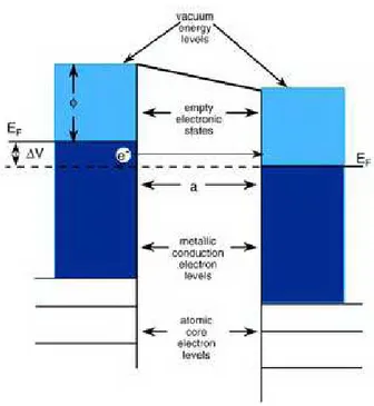
developed by scientists. Before trying to understand the theory of STM, good understanding of the basic principles of vacuum tunnelling is necessary. In vac-uum tunneling the vacvac-uum region acts as a barrier to electrons between the two metal electrodes. In the case of STM, these electrons correspond to the surface and the tip. Fig.2.1 shows this potential barrier schematically. The transmission probability for a wave incident on a one-dimensional barrier can easily be calcu-lated. The solutions of Schr¨odinger’s equation inside a rectangular barrier in one dimension have the form
ψ = e±κz (2.1)
κ2 = 2m(VB− E)
~2 (2.2)
where E is the energy of the state, and VB is the barrier potential . In general
VB may not be constant across the gap, but for the sake of simplicity let us
assume a rectangular barrier. In the simplest case VB is the vacuum level, so for
states at the Fermi level, VB− E is just the work function.
The transmission probability, and hence the tunnelling current, decays expo-nentially with barrier width d as
It ∝ e−kd (2.3)
For tunnelling between two metals with a given voltage difference V across the gap, only the states within eV above the Fermi level can contribute to the tunnelling. Other states cannot contribute either because there are no electrons to tunnel at higher energy, or because there is not any empty state to tunnel into at lower energy.
2.1.1
STM Imaging
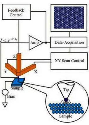
The basic idea underlying STM is quite simple. As illustrated in Fig. 2.2 sharp tip is brought close enough to the surface. At a convenient operating voltage,
Figure 2.1: A one-dimensional tunnelling barrier.
typically 2 mV to 2 V, a measurable tunnelling current, typically between 0.1 nA and 10 nA, is obtained. There are basically two modes of operation of STM. The first and the mostly used one is the constant current mode, in which the tip is scanned over the surface, while the tunnelling current is kept constant by changing the vertical position of the tip with a feedback control circuit. The control circuit achieves this by applying suitable voltages to the z-Piezo. The applied voltage to the piezoelectric crystal simply gives the trajectory of the tip over sample. If a line scan in x-direction is extended to many lines in y direction, an image which consists of a map z(x, y) of the tip position versus lateral position (x, y) is obtained. In the second mode, namely the constant height mode, the tip is kept nearly at a constant height during the scan and the tunnelling current is monitored. The control circuit only keeps the average current constant, It is
plotted against (x, y) to form the image.
Each mode has its own advantages. Constant current mode can be used to scan surfaces which are not atomically flat. On the other hand, the constant height mode allows for much faster scanning of atomically flat surfaces, since only
Figure 2.2: The schematic view of STM principle
the control electronics, not the z-Piezo, must respond to the structure passing under the tip. Fast imaging is important in certain application where researchers can study processes in real time, minimizing image distortion due to piezoelectric creep and thermal drift.
2.1.2
Theory of STM
If the resolution of STM is of the order of a few ˚Angstrom or larger, it is adequate to interpret the image as a surface topograph. However, if the concern is on atomic resolution images, it is not even clear what is meant by a topography. The most reasonable definition is that the topography is a contour of constant charge density from Tersoff-Hamann theory. This contradicts the principle of vacuum tunnelling which says only the electrons near the Fermi level contribute to tunnelling, even though all the electrons below the Fermi level contribute to the
charge density. The following theory developed by the Tersoff and Hamann [7,8] is explanatory even in case of atomic resolution. In first order perturbation theory, the tunnelling current is
I = 2πe
~ X
µ,ν
{f (Eµ)[1 − f (Eν)] − f (Eν)[1 − f (Eµ)]}|Mµν|2δ(Eν+ V − Eµ) (2.4)
where f (E) is the Fermi function, V is the applied voltage, Mµν is the tunneling
matrix element between states ψµ and ψν of the respective electrodes, and Eµ is
the energy of the state ψµ. For most of the purposes, the Fermi functions can be
replaced by their zero-temperature values which are unit step functions. In this case, the above equation, in the limit of small voltage, reduces to
I = 2π
~ e
2V X
µ,ν
|Mµν|2δ(Eµ− EF)δ(Eν − EF) (2.5)
This equation is quite simple. The problem is to evaluate the tunneling matrix elements. Bardeen [27] showed that, under certain assumptions, the tunneling matrix elements can be expressed as
Mµν =
~2
2m Z
dS · (ψµ∗∇ψν − ψν∇ψµ∗) (2.6)
where the integral is over any surface lying entirely within the barrier region. If we choose a plane for the surface of integration, and neglect the variation of the potential in the region of integration, then the surface wave function at this plane can be conveniently expanded in the generalized plane-wave form
ψ =
Z
dqaqe−κqzeiq·x (2.7)
where z is height measured from a suitable origin at the surface, and
κ2q = κ2+ |q|2 (2.8)
A similar expansion applies for the other electrode, replacing aqwith bq, z with
zt− z, and x with x − xt. Here xt and zt are the lateral and vertical components
of the position of the tip, respectively. Then, substituting these wave functions into Eq. 2.6, the matrix elements can be obtained as
Mµν = −
4π2~2
m
Z
Thus given the wave functions of the surface and tip, a simple expression for the tunnelling matrix element and tunnelling current can be found. However, the atomic structure of the tip is generally not known. What would be the criteria in the estimation of the atomic structure of the tip. There are two important points to be considered in this respect. First, the aim is maximum possible resolution, hence the smallest possible tip. Therefore, the ideal STM tip would consist of a mathematical point source of current, whose position is denoted rt. In that case,
Eq. 2.8 for the tunneling current reduces to [27, 28]
I ∝X
ν
|ψν(rt)|2δ(Eν− EF) ≡ ρ(rt, EF). (2.10)
Thus the ideal STM would simply measure ρ(rt, EF), namely the local density of
states at EF(LDOS). LDOS is evaluated for the bare surface. It doesn’t depend
on the complex tip-sample system. The only dependence related to the tip is its position. However, Tersoff-Hamann Theory is valid only for large tip-sample separations. For small separations, a detailed analysis of the tip sample interac-tion is necessary, in order to interpret the images. Because interacinterac-tion is strong enough to affect the measurements. Various studies on this subject [28, 30, 31] have shown that the complex interacting system of the tip and the sample affects the corrugation amplitude.
2.1.3
Scanning Tunnelling Spectroscopy
Scanning tunneling spectroscopy provides information complementary to the in-formation obtained in conventional STM topographic imaging. By measuring the detailed dependence of the tunnelling current on the applied voltage at specific locations of the sample, it is possible to obtain a measure of the electronic density of states of the sample on an atomic scale. If both the energies and the spatial locations of the electronic states are known, direct comparisons with the theory can be made. However, a general theory for the use of STM for the spectroscopy of electronic surface states has not yet been developed. Since the electronic states of the tip and their interaction with the sample surface have to be considered for each sample-tip combination, the evaluation of a general theory is quite difficult.
Tunneling spectroscopy in planar junctions was studied long before STM [34]. However, the development of spatially-resolved spectroscopy with STM stimu-lated the interest in this area. Because of the difficulty of calculating tunneling current I(rt, V ) in general, the studies mostly focused on I(V ), without
consider-ing the dependence to the position of the tip. Selloni et al. [33] suggested that the results of Tersoff and Hamann [8] could be qualitatively generalized for modest voltages as
I(V ) ∝
Z EF+V
EF
ρ(E) T (E, V ) dE, (2.11)
where T (E, V ) is the barrier transmission coefficient, and ρ(E) is the local density of states given by Eq. 2.10 at or very near the surface, and assuming a constant density of states for the tip. However, this simple model does not come up with a straightforward interpretation for the tunnelling spectrum [32]. In particular, the derivative dI/dV has no simple dependence on the density of states ρ(EF + V ).
It can be said that a sharp feature in the density of states of the sample (or tip), at an energy EF + V , will lead to a feature in I(V ) or its derivatives at
voltage V . However, there is a problem with the statements above. The problem is the strong voltage-dependence of the transmission coefficient, T (E, V ), which results in a distortion of features in the spectrum [33]. Stroscio, Feenstra, and coworkers [35] proposed a simple solution to this problem. To eliminate the exponential dependence of T (E, V ) on V , they normalize dI/dV by dividing it by I/V . Therefore the quantity d ln I/d ln V is mostly used for identification of density of states in the STM results.
There is an important problem in tunnelling spectroscopy studies. The elec-tronic density of states of the tip is usually unknown, so it is not so simple to extract the knowledge of the electronic structure of the surface from the spec-troscopy measurements. This problem can be overcome by using the same tip, consequently having a constant background during all measurements. In ac-cordance with the modes of STM imaging, there are various types of scanning tunnelling spectroscopy. These are constant current, constant separation, and variable separation spectroscopy. In constant current spectroscopy, tracing the bias voltage in the specified interval, typically between two values symmetric with respect to zero is necessary, the zero value of the voltage causes the tip to crash
into the sample. Therefore, this mode is experimentally difficult to perform. Con-stant separation spectroscopy is experimentally most preferred one. At a conCon-stant separation, the applied voltage is varied over the specified interval while simul-taneously measuring the tunnelling current. However, in order to correlate the tunnelling spectra with the topograph of the surface, the spectroscopy must be carried out simultaneously with the topographic imaging. This was first achieved experimentally by Hamers et al. [36], and called spatially resolved spectroscopy. Spatially resolved spectroscopy is more complex and experimentally more diffi-cult to achieve, not only because of the necessity of a more complicated control circuit, but due to the need for very stable STM tips, which are very difficult to prepare.
2.1.4
STM on Semiconductors
Scanning Tunnelling Microscope can be used to image only metals, semicon-ductors, and doped insulators, since its operating principle is the tunnelling of electrons. Since its invention, STM has became a widely used instrument to in-vestigate semiconductor surfaces. This is not just because of the power of STM or the necessity to investigate the topographic and electronic properties of these surfaces on an atomic scale, but due to a property of these surfaces that makes them very suitable samples for STM measurements. This property is the re-construction of bulk terminated semiconductor surfaces. Rere-construction of the surface results in large corrugation on the surface, as large as a few ˚A. These large corrugation amplitudes are very easy to detect with STM and can easily be converted into an illustrative gray scale STM image. There are other features of semiconductor surfaces, such as dimers and steps, which have relatively larger scales, that can also be easily resolved. On the other hand, the reconstructed semiconductor surface may exhibit considerable local differences in the electronic structure. .
In the last 30 years, semiconductor technology has continued its fast progress. Silicon based integrated circuits have been developed with extremely high yield. However, the technological thirst for faster and smaller devices enforces scientific
research on semiconductors. SiGe and GaAs heterostructures have begun to form the basis of high-speed semiconductor technology. It is well understood that, to increase the quality and speed of heterostructure based devices, very thin layers, sometimes only a few monolayers of atomic structures are necessary. This can be achieved with Molecular Beam Epitaxy and related techniques . However, al-most all semiconductor surfaces contain single steps separated by a few hundreds of ˚Angstr¨om. Thus without processing of the surface, it is impossible to obtain atomically flat layers having homogenous thicknesses. This problem brings the necessity to investigate the semiconductor surfaces and epitaxial growth at an atomic level. The aim is to decrease the number of steps, which will allow ho-mogenous growth of layers on substrates. By using STM it is possible to observe the mechanisms of growth, and to understand the growth conditions giving the best surfaces. By association of MBE and STM systems, even real-time images of epitaxial growth can be acquired [38].
2.2
Atomic Force Microscopy
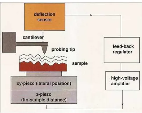
Atomic Force Microscope is invented by Binnig,Gerber and Quate in 1986 as a tool for studying insulating and conducting surfaces. Basic ingredients of an Atomic Force Microscope is shown in Figure 2.3. In fact, the concept of using a force to image a surface is a general one, and can be applied to magnetic and electrostatic forces as well as the interatomic interaction between the tip and the sample. Whatever the origin of the force, all force microscopes have five essential components:
i)A sharp tip integrated to a cantilever spring,
ii)A way of sensing the cantilever deflection,
iii) A feedback system to keep an the deflection at constant level,
iv) A mechanical scanning system (usually piezoelectric crystal based system),
Figure 2.3: The schematic view of an Atomic Force Microscope.
into an image.
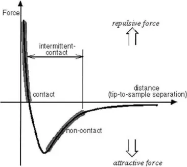
The scanning, feedback and display systems are very similar to those used for STM. An AFM can be operated in three modes: contact mode, non-contact mode and intermittent-contact mode. Figure 2.4 shows the operation regions. In contact mode, the tip is in contact with the sample, and repulsive forces between the tip and sample are measured. The total tip-surface force is the sum of both large range van der Waals (vdW) and short range chemical interactions. For dis-tances below 2 ˚A, the chemical interaction is dominated by the Pauli repulsion and starts to balance the attractive vdW force. Atomic resolution images of lay-ered material such as graphite and boron nitride have been reported [40] but the images do not show individual surface defects, which are routinely observed with the STM. Furthermore, these images persist at large forces (100 nN), where the contact area is predicted to be of the order of 100 ˚A2. These results suggest that
both tip and sample are deformed by the repulsive interaction and that the tip is far from being single atom tip which needed for real atomic resolution. The
Figure 2.4: Interatomic force vs. distance
tip-sample force gradient results in a modification of the effective spring constant of the cantilever. In non-contact AFM mode, the tip is not in contact with the sample, and long-range interaction forces, e.g. vdW, electrostatic, and magnetic force can also be probed. Unlike the contact mode, this method is sensitive to force gradient, rather than the interaction forces between tip and sample. The cantilever is driven to vibrate at its resonance frequency by means of a piezo-electric element, and changes in the resonant frequency as a result of tip-sample interaction are measured. The force gradient between tip and sample, F0 = −∂Fz
∂z ,
results in a modification of the effective spring constant of the cantilever
kef f = k − F
0
(2.12) where k is the spring constant of cantilever in the absence of tip-surface force interaction. An attractive tip-surface interaction with (F0 > 0) will therefore
soften the effective spring constant (kef f < k), whereas a repulsive tip-surface
force interaction (F0 < 0) will strengthen the effective spring constant (kef f >
frequency ω of the cantilever according to ω = (kef f m ) 1/2 = [(k − F 0 ) m ] 1/2 = (k m) 1/2(1 − F 0 k ) 1/2 = ω 0(1 − F0 k ) 1/2 (2.13)
where m is an effective mass and ω0 is the resonance frequency of the cantilever
in the absence of force gradient. If F0 is small relative to k then the Eq. (2.12) can be approximated by ω ≈ ω0(1 − F0 2k) (2.14) and therefore ∆ω ω0 ≈ −F 0 2k (2.15)
and attractive force (F0 > 0) will therefore lead to a decrease of the resonant
frequency (ω < ω0), whereas a repulsive force (F
0
< 0) will lead to an increase
(ω > ω0). The above approximation can be to applied to small cantilever
oscil-lation amplitude A, compared to the length scale of the tip-surface interaction force. However most non-contact AFMs operate at very large oscillation ampli-tudes, 1-60 nm!. If the maximum restoring force is greater than the maximum attractive force, kA À Fmax, and the cantilever is driven at its resonance
fre-quency with large oscillation amplitude, the shift of resonance frefre-quency 4ω can be described by the following perturbation equation:
4ω ω0 kA = I dϕ 2πF (z + Acosϕ)cosϕ (2.16) where the force F is integrated over one oscillation cycle and z is the time averaged position of the tip.
Different methods are used for measurement of the resonance frequency shift, ∆f . A method which is called slope detection method, the cantilever is driven by means of a piezoelectric element with a typical amplitude at the tip on the order of 1-10 nm at a determined frequency ωd, the amplitude change or phase
shift of the vibration as a result of the tip-surface force interaction is measured with the deflection sensor and a lock-in amplifier. A feedback loop adjusts the tip-surface separation by maintaining a constant force gradient. Another method which is proposed by Albrecht et al. [12] in 1991 is called frequency modula-tion (FM) technique, oscillamodula-tion of the cantilever is maintained at resonance by
Figure 2.5: The schematic view of tip sample interaction in dynamic mode
a feedback loop using the signal from deflection sensor. Change in the oscillation frequency, caused by variations of the force gradient of the tip sample interaction, are directly measured by a frequency counter or FM discriminator. To achieve the highest possible detection sensitivity for a given free oscillation amplitude A0, the
cantilever should have a small spring constant k and a high resonance frequency
f0, in addition, a high Q-factor for the cantilever is desirable, which can only be
achieved in the vacuum condition. Oral et al. [41] proposed a new method using sub-˚Angstrom oscillation amplitude of the order of 0.25˚A and below-resonance which enables the researchers direct measurement of force gradients acting on the tip due to tip- surface interaction. In this limit, the measurement is linear and quasi-static. This technique overcomes some of the limitations of the nc-AFMs, which use large amplitude frequency modulation techniques. While providing high resolution images these techniques have limitation to give quantitative spec-troscopic data in atomic manipulation experiments and in measuring the nature of dissipative processes. This is because the measured parameter(frequency shift, ∆f ) is not related to the interaction energy or force in a simple manner at large oscillation amplitudes. Mathematical deconvolution is needed in order to extract the force, which relies on a number of assumptions such as the harmonic motion of the lever, a conservative interaction potential and general reversibility of the interaction. In small amplitude nc-AFM technique, the maximum possible energy
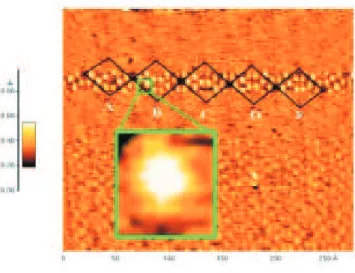
Figure 2.6: The first atomic resolution image obtained in UHV using nc-AFM. Image of Si (111)-(7×7) surface [13]
input into the tip-sample interaction region is of the order of only 10−3eV per
cycle as opposed to several eV in the case of large amplitude, resonance enhance-ment technique. In addition, a high Q-factor cantilever and vacuum condition is no longer a necessary, therefore this technique promises to explore and map the mechanics of matter at the nano-and atomic scale even in ambient condition and under liquids [42, 44].
In intermittent-contact atomic force microscopy, which is similar to nc-AFM, the cantilever tip is brought closer to the sample so that the bottom of its travel it just barely hits, or taps, the sample. In intermittent contact atomic force microscopy the cantilevers oscillation amplitude changes in response to tip-to-sample spacing similar to nc-AFM. An image representing surface topography is obtained by monitoring these changes. Some samples are best handled using IC-AFM instead of contact or non-contact AFM. IC-AFM is less likely to damage the sample than contact AFM, because it eliminates lateral forces (e.g. friction) between the tip and the sample. In general, it has been found that IC-AFM is more effective than nc-AFM for imaging larger scan sizes that may include greater variation in sample topography.
2.2.1
Nature of contributing forces in AFMs
Unlike the tunneling current, which has very strong distance dependence, Fts
has long and short range contributions. We can classify the contributions by their range and strength. In vacuum, there are van der Waals, electrostatic and magnetic forces with a long range (up to 100 nm) and chemical forces with a short range (fractions of nm). In ambient conditions, meniscus forces formed by adhesion layers on tip and sample (water and hydrocarbons)may also be present.
The van der Waals interaction is caused by fluctuations in the electric dipole moment of atoms and their mutual polarization. For a spherical tip with radius R next to a flat surface (z is the distance between the plane connecting the centers of the surface atoms and the center of the closest tip atom), the van der Waals potential is given by [59]:
UvdW = −
AHR
6z . (2.17)
The Hamaker constant AH depends on the tip and the sample material,
(atomic polarizibility and density). For most solids and interactions across vac-uum, AH is of the order of 1 eV. The van der Waals interaction can be quite
large, the typical radius of an etched metal tip is 100 nm and with z=0.5 nm, the van der Waals energy is about 30 eV, and the corresponding force is about 10 nN.
When the tip and sample are both conductive and have an electrostatic poten-tial difference, electrostatic forces are important. For a spherical tip with radius
R, the electrostatic force is given by [60]:
Felectrostatic(z) = −
π²0RU V2
z . (2.18)
Like the van der Waals interaction, the electrostatic interaction can also cause large forces- for a tip radius of 100 nm, U= 1 V and z=0.5 nm, the electrostatic force is about 5.5 nN. Electrostatic forces can also arise in the imaging of ionic crystals, where the envelope of the electrostatic field has an exponential distance dependence.
Chemical forces are more complicated. Reasonable empirical model potentials for chemical bonds are Morse potential [59],
VM orse = −Ebond[2e−κ(κ−σ)− e−2κ(z−σ)] (2.19)
and the Lennard-Jones potential:
VLennard−Jones = −Ebond(2
z6
σ6 −
z12
σ12) (2.20)
The potential describe a chemical bond with bonding energy Ebond and
equilib-rium distance σ . The Morse potential has an additional parameter, namely, a decay length κ. While the Morse potential can be used for a qualitative descrip-tion of chemical forces, it lacks an important property of chemical bonds. The bonding strength of chemical bond, especially covalent bonds, shows an inherent angular dependent .
2.2.2
Sensitivity of AFMs
From Hooke’s Law (F=-k.x) we can see that the smallest force that can be mea-sured depends on the spring constant of the lever, k, and the sensitivity of the displacement detection system to lever motion. The better the sensitivity of the deflection detection system, the smaller the displacement that can be measured, and hence the smaller the force that can be measured for a given lever spring con-stant. Therefore the lever and the displacement detection system are the most crucial factors for the sensitivity of an AFM. Initially cantilevers were home made, with the first one being a piece of gold foil with a diamond fragment glued on it, to act as a tip. However, as Binniget al. [3] suggested, microfabrication became a simple and convenient way to mass produce levers with built in tips. Cantilever beam and V- shaped cantilevers can be microfabricated from silicon, silicon oxide, or silicon nitride with integral tips, and the force constant and resonant frequency can be reproducibly microfabricated. For contact force microscopy, levers with low force constants (< 1N/m) are used to prevent sample damage and to give good sensitivity for the force measurement. Whereas, levers with force constants of a few tens of N/m are needed for noncontact force microscopy. This is to
prevent ’snap in’, and to increase the resonance frequency of the levers used in FM-AFM work, which improves the system’s displacement sensitivity. For any deflection detection system, the noise in the system limits its force sensitivity. The noise can come from several parts of the deflection detection system. For an STM based system the noise is predominantly 1/f noise. For an interferometer based system, the main sources of noise are the shot noise in the photodetectors and laser noise due to variations in the power and the phase of the laser. The noise due to thermal oscillations of the lever may also be significant for levers with low spring constants. In Chapter 3, the sources of noise and attempts towards reducing the noise to achieve the best force gradient sensitivity will be explained. Several different methods of measuring lever displacement measurements have been employed in AFMs. In the first AFM built by Binnig et al. [3], an STM was used to measure lever displacement. The STM tip was situated just above the cantilever, directly behind the tip. Since the tunnelling current varies exponen-tially with distance, the STM is a very sensitive method to measure deflections of the lever. Deflections of less than 10−2 ˚A can be measured. However,
prob-lems associated with keeping the cantilever and tip clean reduced the reliability of this method in air. There are strong interactions between the lever and the STM tip during tunnelling, which reduce the lever’s resonant frequency, and may alter its deflection. Since the STM tip must remain in close proximity to the cantilever this method is not well suited to use in nc-AFM where large vibration amplitudes are often used. Neubauer et al. [44] used the back of a cantilever as one plate in a capacitor. As the lever bends the change in its position results in a change in the capacitance. The variation of the capacitance is measured and used to calculate the deflection of the lever. This technique relies on a uniform smoothness and distance between the plates. The sensitivity of this technique is around 10−2√˚A
Hz. Optical techniques are generally more reliable and easier
to implement than STM, and they are also less sensitive to the roughness of the lever. There are several different optical methods that have been used to measure cantilever displacement. In the beam deflection method introduced by Meyer and Amer [42], a focused laser beam is reflected off the back of the cantilever, and the position of the beam is monitored using a position sensitive photodiode. As the lever bends, the reflected beam moves across the photodiode, one segment
collects more light than the other, and a differential amplifier produces an output current proportional to the lever displacement. If a quadrant photodiode [47] is used, then information about movement of the lever parallel to the surface can be obtained along with topographic information. The torsion of the lever can be related to the friction forces on the tip. This detection method is independent of optical path length changes, but not to the thermal or mechanical drift in the direction perpendicular to the optical beam. The minimum detectable signal using beam deflection is about 4 × 10⁻³√˚A
Hz.
Sarid et al. [61] used the sensitivity of a laser diode to optical feedback to measure cantilever displacement. The laser diode is placed close to the back of the lever, and, as the lever moves, the combined reflectivity of the front face of the laser cavity and the lever changes. The light reflected back into the laser diode changes the output power of the laser. This is measured by a photodetector which is integrated into the laser diode. This technique removes the need for extra optical components and alignment of the laser diode with the lever is straight forward. However, the non linear nature of the laser optics means that this method is only suitable for measuring small lever displacements accurately. The minimum detectable signal using this system is about 3 × 10⁻³√˚A
Hz.
In a heterodyne interferometer, as used by Martin et al. [43], the laser beam is split into two components by a beam splitter. One of the beams which acts as, the reference beam, follows a fixed path to the photodetector. The other beam passes through an acousto-optic modulator and has its frequency shifted. This signal beam is reflected from the back of the lever and into the photodetector, where it interferes with the reference beam. As the lever bends, the path of the signal beam changes, so its phase relative to the reference beam changes. This is detected and used to calculate the displacement of the lever. Heterodyne interferometers have a sensitivity of about of 5 × 10⁻⁵√˚A
Hz, and are insensitive to
changes in the optical path length.
A typical homodyne interferometer used as a displacement sensor in an AFM consists of a laser diode coupled to a single mode fiber optics cable [48]. The end of the fibre is positioned a few microns from the back of the cantilever. The
laser beam is split into two equal parts by a 2 × 2 directional fiber coupler. One half of the light goes to a reference photodiode and the other half goes down the fiber to the lever. About 4%. of the light is internally reflected from the fiber-air interface, and the rest is directed at the back of the lever. Some of the light reflected from the back of the lever re-enters the fiber. This signal passes back through the directional coupler, and the interference signal of the two beams is detected at the signal photodiode. The output of the signal photodiode can be used directly as the force signal, but better sensitivity is achieved by dividing or subtracting the output of the signal photodiode by the output of the reference photodiode. This cancels out laser noise from the signal. The small cavity im-proves the D.C. stability of the interferometer. This type of interferometer has a sensitivity of 1 × 10⁻⁴√˚A
Hz. Sch¨onenberger and Alvarado [62] used a differential
interferometer, which makes use of beam polarization. A laser beam consisting of two mutually orthogonal polarization states is split into two spatially separate beams, the reference and sensor beams, by passing it through a calcite crystal. Both beams are reflected from the back of the cantilever. The reference beam is reflected from the fixed base of the cantilever, while the sensor beam is re-flected from the lever just behind the tip. The two rere-flected beams are detected by photodiodes, and the displacement of the lever is calculated from their phase difference. The output from the differential system has a large common mode rejection that cancels out most of the laser noise. The sensitivity of this interfer-ometer is about 6 × 10⁻⁴√˚A
Hz. Jarvis et al. [49] used a combination of heterodyne
and differential interferometers, which used two orthogonally polarized beams, one frequency shifted with respect to the other. This give the system the benefits of both types of interferometer, and a sensitivity of 1 × 10⁻⁴√˚A
Hz.
Silicon exhibits a strong piezoresistive effect, and this has been used to make cantilevers with a built in displacement sensors [95]. A U-shaped lever with a piezoresistor built into both legs can be easily microfabricated. The lever is used as part of a Wheatstone bridge, and the change in resistance of the cantilever as it bends, is used to measure its deflection. This type of deflection detection removes the need for a laser or any optics, and is simple to implement since it requires no alignment. The sensitivity of piezoresistive levers is of the order of
Figure 2.7: The methods of cantilever deflection measurement 1 × 10⁻³√˚A
Hz. Giessibl and coworkers [13] use qPlus sensor made from a quartz
tuning fork. The qPlus sensor has stiffness of about 1800N/m. One of the prongs is fixed to a large substrate and a tip is mounted to the free prong. Because the fixed prong is attached to a heavy mass, the device is mechanically equivalent to a traditional cantilever. Bending the free prong of the tuning fork create current proportional to its displacement. The sensitivity of The qPlus sensor is of the order of 3 × 10⁻⁴√˚A
Hz at room temperature. The Schematic view of different
methods of cantilever deflection measurement is shown in Fig. 2.7.
2.3
Pathway from atomic resolution imaging to
single atom manipulation
2.3.1
Atomic resolution imaging using STM
The STM allowed the first atomic resolution real space images of surfaces to be taken. Demonstrating this ability, Binnig and Rohrer [1, 2] showed an atomic
resolution image of the Si(111)-(7×7) surface reconstruction. It had not been possible to unambiguously identify the exact reconstruction until the STM was used to image the surface and show where individual adatoms were positioned. Atomic resolution images of close packed metal surfaces soon followed. Au(111) was imaged by Hallmark et al. [96], and Winterlin et al. [29] imaged Al(111). Both of these surfaces were found to have corrugation heights of 0.3 ˚A. For these surfaces the corrugations of the Fermi level LDOS are too small to be seen experimentally, and He scattering experiments show a corrugation height an order of magnitude smaller than that seen in the STM images. Winterlin et al. [29] attribute the fact that atomic resolution can be seen on close packed surfaces due to adhesive tip-surface interactions causing an elastic deformation of the end of the tip. Besides imaging metal surfaces, STMs were used to image graphite and semiconductor surfaces, such as GaAs(110), and Si(100). Graphite was one of the first substrates to be imaged using STM in air [2]. The problem with the images of graphite was that the surface corrugations seen were much larger than the 0.8 ˚A expected from calculations, and the tunnel barrier height was much lower than expected. Tersoff [8] attributed the huge corrugations in layered materials to an anomalous corrugation of the contours of constant LDOS at the Fermi level due to the special electronic structure of layered materials. He also showed that the contours are equally spaced and independent of distance from the surface, and concludes that the STM image is likewise independent of distance i.e. independent of current at constant voltage. However, as Soler et al. [58] point out, the corrugations increase with increasing tunnel current, at constant voltage. They suggested that elastic deformations of the surface, when low bias voltages and high tunnel currents are used, increase the observed corrugations. In a reply to this paper Pethica [63] pointed out that the force of the contact is large enough that a contact area much larger than a single atom must be expected, and that shearing of the graphite planes is likely to happen with the large pressure exerted on the top layers. Sliding the top graphite plane in and out of registry with the layers below it would result in an image with a periodic structure on an atomic scale, without resulting in true atomic resolution. Mamin et al. [77] attributed the giant corrugations to a large deformation of the graphite surface, in this case caused by the presence of a contaminant layer between the tunnelling tip and the
sample, which required the tip to be force into the sample for a tunnel current to be detected, and results in a contact area larger than atomic dimensions. This would also explain the reduced tunnel barrier heights that were often seen, since the tip has to move further than expected for a given increase in tunnel current. They also noted that in UHV the experimentally measured corrugations were 0.9 ˚
A . This illustrates the need for the use of clean surfaces with clearly defined surface structures to make interpretation of images more straight forward. The next step on from imaging surfaces was to image adsorbates on surfaces. Eigler and Schweizer [17] spectacularly showed that at 4K they could not only image Xe atoms on Ni(110), but they could also move the atoms into the shapes of letters by lowering the tip over the atom and moving it to the desired position. Following on from this Crommie, Lutz and Eigler [19] showed that by moving Fe atoms into a circle on a Cu(111) surface the local density of states inside the circle is dominated by the eigen state density expected for an electron trapped in a circular 2D box. This means that rather than imaging the positions of the atoms in the surface inside the circle of Fe atoms, the STM image is dominated by the electronic structure. Other adsorbate systems have also been imaged at room temperature, such as oxygen on Cu(110) and Ni(110), and sulphur on Pt(111). These papers also highlight the need to know what the atom on the end of the tip is, and show how that effects the STM images taken. McIntyre et
al. [64] imaged the (√3 ×√3)R30◦ sulphur structure on Pt(111), and discovered
that the corrugation heights of the images they took changed after pulsing the tip at 0.7 V. Imaging the area where the tip pulse occurred showed that there were several missing Sulphur atoms. They concluded that transfer of sulphur atoms to the tip had occurred, and this resulted in the image corrugations seen increasing from 0.2 nA to 1.2 nA. Ruan et al. [65] imaged the oxygen induced (2×1) reconstruction on both Cu(110)and Ni(110). The (2×1) reconstruction consists of rows of alternating metal and oxygen atoms in the [001] direction, spaced at one row for every two bulk lattice rows in the [1¯10] direction. The images of the rows show a periodicity compatible with imaging either the oxygen or the metal atoms. The Oxygen atom has been identified as occupying the long bridge position between the Cu atoms in the [001] direction, and so if the Oxygen atoms were imaged they would be in line with the Cu atoms in the [1¯10]
![Figure 2.9: Atom interchanging using room temperature FM-AFM. (Adapted from [100]).](https://thumb-eu.123doks.com/thumbv2/9libnet/5842727.119785/55.892.299.658.185.438/figure-atom-interchanging-using-room-temperature-afm-adapted.webp)