PHYSICS AND APPLICATIONS OF GOUPLED-CAVITY
PHOTONIC CRYStALS
A THESIS
SU B M ITTE D T O THE D EP A R TM E N T OF PH YSICS
AND TH E INSTITUTE OF ENGINEERING AND SCIEN CE
O F B iL K E N T U N IVERSITY
IN PA R TIA L FU L FIL LM E N T OF TH E R E Q U IR E M E N T S
FOR TH E DEGREE OF
D O C T O R OF PH ILO SO PH Y
M E H M E T BAYINDIR
M A Y , 2002
€ iC ¥ 3 3 5 P ^ 2 ¥ B 3 B2.002
PHYSICS AND APPLICATIONS OF COUPLED-CAVITY
STRUCTURES IN PHOTONIC CRYSTALS
A THESIS
SUBMITTED TO THE DEPARTMENT OF PHYSICS AND THE INSTITUTE OF ENGINEERING AND SCIENCE
OF BiLKENT UNIVERSITY
IN PARTIAL FULFILLM ENT OF THE REQUIREM ENTS FOR THE DEGREE OF
DOCTOR OF PHILOSOPHY
By
M e h m e t B a y i n d i r
ß O ( » 9 0 4 9
б< с - ч э з л
. P itî'l·
I certify that I have read this thesis and that in my opinion it is fully adequate, in scope and in quality, as a dissertation for the degree of Doctor of Philosophy.
Prof. Ekinel Ozh
I certify that I have read this thesis and that in rny opinion it is fully adequate, in scope and in quality, as a dissertation for the degree of Doctor of Philosophy.
Prof. Alexander S. Shumovsky
I certify that I have read this thesis and that in my opinion it is fully adequate, in scope and in quality, as a dissertation for the degree of Doctor of Philosophy.
I certify that I have read this thesis and that in rriy opinion it is fully adequate, in scope and in quality, as a dissertation for the degree of Doctor of Philosophy.
Asst. Prof. SerdaiK)zgelik
I certify that I have read this thesis and that in my opinion it is fully adequate, in scope and in quality, as a dissertation for the degree of Doctor of Philosophy.
Approved for the Institute of Engineering and Science:
^rof. iVIehmet Baray,
Abstract
PHYSICS AND APPLICATIONS OF C O U P LE D -C AVITY STRUCTURES IN PHOTONIC CRYSTALS
M e h m e t Ba y i n d i r
Ph. D. in Physics
Supervisor: Prof. Ekmel Ozbay May, 2002
We proposed and demonstrated a new type of propagation mechanism for the electromagnetic waves in photonic band gap materials. Photons propagate through coupled cavities due to interaction between the highly localized neighboring cavity modes. We reported a novel waveguide, which we called coupled-cavity waveguide (CC W ), in two- and three-dimensional photonic structures. By using CCWs, we demonstrated lossless and reflectionless waveguide bends, efficient power splitters, and photonic switches. We also experimentally observed the splitting of eigenmodes in coupled-cavities and formation of defect band due to interaction between the cavity modes.
We reported the modification of spontaneous emission from hydrogenated amorphous silicon-nitride and silicon-oxide multilayers with coupled Fabry-Perot microcavities. We observed that the spontaneous emission rate is drastically enhanced at the coupled- microcavity band edges due to very long photon lifetime.
We also simulated our photonic structures by using the Transfer-Matrix-Method (TMM ) and the Finite-Difference-Time-Domain (FDTD) method. The tight-binding (TB) approach, which was originally developped for the electronic structure calculations, is applied to the photonic structures, and compared to our experimental results. The measured results agree well with the simulations and the prediction of TB approximation. The excellent agreement between the measured, simulated, and the TB results is an indication of potential usage of TB approximation in photonic structures.
Our achievements open up a new research area, namely physics and applications of coupled-cavities, in photonic structures. These results are very promising to construct for the future all-optical components on a single chip.
K e y w o rd s : Photonic Crystal, Photonic Band Gap (PBG), Defect, Fabry-Perot Cavity, Waveguide, Transfer Matrix Method (TM M ), Finite-Difference-Time-Domain (FDTD) Method, Tight-Binding (TB) Approximation, Coupled-Cavity Waveg uides (C C W ), Power Splitter, Photonic Switches, Wavelength- Division-Multiplexing (W DM ), Spontaneous Emission.
ö zet
FO TO N IK k r i s t a l l e r d e k i ETKİLEŞİM Lİ-CAVİTE
YAPILARININ FİZİĞİ VE U Y G U L A M A LA R I
M e h m e t Ba y i n d i r
Fizik Bölümü Fizik Doktora Tez Yöneticisi: Prof. Ekmel Özbay
Mayıs 2002
Elektromanyetik dalgaların fotonik kristaller içerisindeki hareketi üzerine yeni bir mekanizma önerildi ve deneysel olarak doğrulandı. Önerilen mekanizmada, fotonlar yerelleşmiş kavite modları üzerinden, modlar arasındaki etkileşmeden dolayı, atlayarak hareket edebilir. Bu yöntemin iki ve üç boyutlu fotonik kristallerde kullanılmasıyla, kayıpsız yönlendiricilerin, verimli elektromanyetik güç bölücülerin, ve optik anahtarların mümkün olabileceği gösterildi. Yeni geliştirilen bu yapılar sayesinde, ışığın, optik devrelerde kayıpsız ve geriyansımasız yönlendirilebilmesi mümkün hale gelmektedir.
Hidrojene edilmiş amorf silikon-nitrat ve silicon-oksit bazlı çok katmanlı etkileşimli- kavite yapılarda spontane ışınımların modifikasyonları, artırılması veya azaltılması, incelendi. Spontane ısınım, etkileşimli-kavite bandının kenarlarında gereğinden daha fazla arttığı gözlendi. Bu sonuç, foton grup hızlarının band kenarlarında çok azalmasından kaynaklandığı önerildi.
yöntemleri kullanılarak, deneydeki yapıların simulasyonları yapıldı. Ayrıca, elektronik sistemlerde başarı ile uygulanan sıkı-bağlanma yöntemi, fotonik yapılara uygulandı. Deney ve teorik sonuçların birbirleriyle çok iyi uyuşması, sıkı-bağlanma yönteminin fotonik yapılarda da başarıyla kullanılabileceği gösterildi.
Bulduğumuz bu sonuçlar fotonik yapıların incelenmesinde ve kullanılmasında yeni bir araştırma alanın doğmasına yol açmıştır. Ayrıca bu sonuçlar ileride yapılacak hepsi-optik yapıların tasarlanmasında kullanılabilecektir.
A n a h ta r
sözcü k ler: Fotonik Kristal, Fotonik Bant Aralığı, Düzensizlik, Fabry- Perot Kavitesi, Dalga Kılavuzu, Transfer Matris Metodu (TM M ), Sıkı-Bağlanma Yaklaşımı, Zaman Bölgesinde Sonlu Farklama, Etkileşimli-Kavite Dalga Kılavuzu, Fotonik Güç Bölücü, Spontane Işınım.
Acknowledgement
It is my pleasure to express my deepest gratitude to Prof. Ekmel Ozbay for his guidance, helpful suggestions, and fruitful discussions during last three years. I feel myself lucky to have a chance to study with him. Beyond his invaluable contribution to my academic personality, I also learned a lot from his superior motivations:
Sky is the limit!
I would like to thank to all members of the physics department for their continuous help and moral support. My special thanks to Prof. Zafer Gedik, Prof. Bilal Tanatar, and Prof. Salim Ciraci for their guidance and motivations. Thank you Emine Abla, you make my life easier all the time. I would also thank to members of the Bilkent photonic band gap group, Burak Temelkuran, Ertugrul Cubukcu, Irfan Bulu, S. Sena Akarca, and Koray Aydin, for their invaluable contributions to the experiments and simulations.
I am also indebted to my residence-mate Necmi Bıyıklı for his understanding, help, moral support, and making my life joyful and easier during last five years.
Finally I would express my endless thank to my family for their understanding and moral support. Thank you my fiance, Esra Eren. I can not imagine to finish all my achievements without your endless support.
Contents
A b s tr a c t Ö zet ii A c k n o w le d g e m e n t ii 1 In tr o d u c tio n 2 2 T ig h t-B in d in g A p p r o x im a tio n 62.1 Localized Coupled-Cavity Modes in Photonic C rystals... 8 2.1.1 Photonic Molecules: Eigenmode S plittin g... 8 2.2 A Novel Waveguiding M e ch a n ism ... 10
2.2.1 Dispersion Relation and Group Velocity 11
2.2.2 Photon Lifetime and D isp ersion ... 12
2.3 Summary 13
3 P h y sics a n d A p p lica tio n s o f CCWs 15
3.1 Analysis of Localized Coupled-Cavity Modes: Experiment versus Theory 17
CONTENTS
3.1.1 Experimental S e tu p ... 17
3.1.2 Eigenmode S p l it t i n g ... 19
3.1.3 Delay Time M easurem ents... 21
3.2 Coupled-cavity waveguides ( C C W s ) ... 21
3.2.1 Transmission Measurements and FDTD Simulations... 21
3.2.2 Dispersion Relation, Group Velocity, and Photon Lifetime 25 3.3 Splitters and Switches 25 3.4 Summary 27 4 C oup led -C avities in 3D P hotonic C rystals 29 4.1 3D Layer-by-Layer Photonic C r y s ta ls ... 30,
4.2 Mode Splitting . . . . ; ... 31
4.3 Waveguide and Waveguides B e n d s... 33
4.3.1 Transmission M easurem ents... 34
4.3.2 Phase M easurem ents... 36
4.4 Heavy Photons at Coupled-Cavity Band E d g e s... 37
4.4.1 Box-like C a v it ie s ... 37
4.4.2 Single Rod Removed C a v i t i e s ... 41
4.5 Summary 42 5 H igh ly Confined P hotonic C rystal W aveguides 43 5.1 Experimental S e tu p ... 44
CONTENTS 111
5.2 Waveguides and Waveguide B e n d s... 45
5.3 Power S p lit t e r s ... 47
5.4 Theoretical Model: Tight-binding a n a ly s is ... 48
5.5 Dropping of electromagnetic waves through localized modes: W DM a p p lica tio n s ... 50
5.6 Summary 54 6 C oupled optical microcavities 55 6.1 Fabrication of coupled microcavity structures 56 6.2 Analysis of coupled microcavity structures: Experiments versus TM M S im u la tio n s ... 58
6.2.1 Eigenmode S p l it t i n g ... 58
6.2.2 Formation of Cavity B a n d ... 61
6.3 Modification of spontaneous e m is s io n ... 63
6.3.1 Photoluminescence from Single Microcavity 64 6.3.2 Photoluminescence from Coupled Microcavity S tru ctu re s... 65
6.4 Summary 67
List of Figures
1.1 Schematic drawing of photonic band gap effect in photonic crystal due to
periodic dielectric function. 3
1.2 Annual publications on photonic band gap materials in Science Citation
Index journals. The doubling time is around 25 months. 4
2.1 Schematics of a coupled-cavity structure in a two-dimensional photonic c r y s t a l ... 7 2.2 Calculated dispersion relation and group velocity as a function of
wave vector k... 12
2.3 Calculated delay time and dispersion as a function of normalized frequency
u. 14
3.1 Schematic drawing of planar and coupled-cavity waveguides in photonic crystals... 16 3.2 Schematics of the experimental setup for measuring
transmission-amplitude and transmission-phase spectra... 17 3.3 Measured and calculated transmission spectra by using FDTD method for
a single cavity, two coupled cavity, and three coupled cavity structures. . 18
3.4 Measured delay time characteristics of the corresponding coupled-cavity structures, namely, single cavity, two coupled-cavity, and three coupled- cavity. ... 20 3.5 Measured and calculated transmission spectra of the straight coupled-
cavity waveguide which is generated by removing 10 adjacent rods from
the crystal. 22
3.6 Measured and calculated transmission spectra of the zig-zag coupled-cavity waveguide which contains 16 cavities... 23 3.7 Comparison of the measured and calculated dispersion relation, group
velocity, and delay time corresponding to the straight C C W ... 24 3.8 Measured and calculated of transmission spectra of a Y-shaped
coupled-cavity based splitter... 26 3.9 Measured and calculated transmission characteristics of a coupled-cavity
switching structure. ... 27
4.1 Schematic drawing of the coupled-cavity structures in a layer-by-layer
photonic crystal. 31
4.2 Transmission characteristics along the stacking direction of the photonic crystal... 32 4.3 Defect characteristics of the laser-micromachined alumina photonic crystal. 33 4.4 Transmission amplitude as a function of frequency for a straight and zig
zag waveguides... 35 4.5 Dispersion diagram of the waveguiding band predicted from the
transmission-phase measurements and calculated by using tight-binding formalism with k — —0.047... 36
4.6 Schematics of the box-like cavity in 3D layer-by-layer photonic crystals. . 38
LIST OF FIGURES VI
4.7 Photon lifetime, = dipjOuj^ as a function of frequency. 39
4.8 Transmission through a ten unit cell periodic coupled defects. 40 4.9 The measured and calculated delay time for the single rod removed CCW. 41
5.1 Schematic drawing of a new type of waveguide structure in 3D layer-by-layer photonic crystals... 44 5.2 Experimental setup for measuring the transmission-amplitude and
transmission-phase spectra of the straight, bended waveguides, and the power splitter structure... 45 5.3 Transmission amplitude measured from a single rod removed waveguide
structures... 46 5.4 Measured transmission characteristics of the 90-degree bended waveguide. 47
5.5 Measured transmission spectra for the splitter structure. 48
5.6 Schematic drawing of coupled-cavities in highly confined waveguides. 49 5.7 Dropping of electromagnetic waves in 3D photonic crystal structures. . . 51 5.8 Measured transmission characteristics of the demultiplexing structure in
Fig. 5.7(a). 52
5.9 Measured transmission characteristics of the demultiplexing structure in
Fig. 5.7(b). 53
5.10 Measured transmission characteristics of the donor-type demultiplexing
structure. 54
LIST OF FIGURES Vll
6.2 Schematics of the fabricated coupled optical microcavity structures which are constructed by depositing silicon-oxide and silicon-nitride multilayers on the glass substrates... 57 6.3 Measured and calculated transmission spectra for a distributed Bragg’s
reflector (DBR), single cavity, two coupled cavity, and three coupled- cavity structures... 59 6.4 Calculated held patterns of single cavity and two coupled cavities as a
function of the position. 60
6.5 Measured (dotted) and calculated (solid) transmission through a coupled microcavity (CM C) structure which contains of 7 coupled cavities... 62 6.6 Calculated dispersion relation and group velocity of the CMC structure
as a function of wavevector k... 63
6.7 Schematic drawing of a coupled-microcavity structure and the experimen tal setup for measuring the photoluminescence spectra... 65 6.8 Measured transmission and photoluminescence spectra of a hydrogenated
amorphous-silicon-nitride Fabry-Perot m icrocavity... 66 6.9 Measured photoluminescence intensity as a function of wavelengths for
various collecting angles 9... 66
List of Tables
3.1 Comparison of the resonant frequencies of three coupled cavities obtained by measurements, the FDTD simulations, and the tight-binding (TB) approximation. ... 19
4.1 The measured and calculated values of resonant frequencies for the crystal with three defective unit cells... 32
6.1 Comparison of the resonant frequencies of three coupled cavities obtained by measurements, the transfer matrix method simulations (TM M ), and
Chapter 1
I
ntroduction
If only it were possible to maike dielectric materials in which electromagnetic waves cannot propagate at certain frequencies, all kinds of almost-magical
things would be possible.
John Maddox, Nature 3 4 8 , 481 (1990)
P
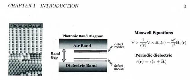
HOTONIC crystals, also known as photonic band gap (PEG) materials, are artificial dielectric or metallic structures in which the refractive index modulation gives rise to stop bands for electromagnetic waves (EM) within a certain frequency r a n g e . I n analogy with electronic band-gaps in semiconductors, these structures are called photonic band gap (PEG) materials or photonic crystals.The easiest way to understand the behavior of light in a photonic crystal is to compare it to the movement of electrons in a semiconductor. In a silicon crystal, the atoms are arranged in a diamond-lattice structure, and electrons moving through this lattice experience a periodic potential as they interact with the silicon nuclei via the Coulomb force. This interaction results in the formation of allowed and forbidden energy states. No electrons will be found in an energy range called the forbidden energy gap or simply
CH A PTE R !. INTRODUCTION iQtOrfej t i f i 1 1 i: : t t t u t n n t z t Z t W t Z t Z Z:
t z z z t u z z z
t Z n % z M z z z^ t t z z t z z z
Photonic Band Diagram
Air Band Band Gap A V Dielectric Band defect modes defect modes Maxwell Equations V X X H^(r) = i H^.(r) f(r) c-Periodic dielectric e-(r) = 6(r + R )
Figure 1.1: Schematic drawing of photonic band gap effect in photonic crystal due to periodic dielectric function.
the band gap.
Now consider photons moving through a block of transparent dielectric material that contains a number of tiny air holes arranged in a lattice pattern. To a photon, this contrast in refractive index looks just like the periodic potential that an electron experiences travelling through a silicon crystal. Indeed, if there is large contrast in refractive index between the two regions then most of the light will be confined either within the dielectric material or the air holes. This confinement results in the formation of allowed energy regions separated by a forbidden region, i. e., photonic band gap (See Fig. 1.1).
It is possible to create energy levels in the photonic band gap by changing the size of a few of the air holes in the material. This is the photonic equivalent to breaking the perfect periodicity of the silicon-crystal lattice. In this case, the diameter of the air holes is a critical parameter, together with the contrast in refractive index throughout the material.
However, the technological challenges restrict the experimental demonstrations and relevant applications of these crystals to millimeter wave and microwave frequencies.^"'^ It has taken over a decade to fabricate photonic crystals that work in the near-infrared and visible regions of the spectrum. The remaining challenge has been to find suitable
CHAPTER 1. INTRODUCTION
j'(Y ear)
Figure 1.2: Annual publications on photonic band gap materials in Science Citation Index journals. The doubling time is around 25 months.
materials and processing techniques to fabricate structures that are about a thousandth the size of microwave crystals.
To be able to create photonic crystals for optical devices, we need to use state-of- the-art semiconductor-microfabrication techniques with their associated high production costs and investment. For this reason computer modelling of prospective photonic- crystal structures is also a very important area of research, as it may prevent expensive fabrication errors later.
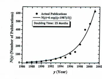
Since the first paper about PEG materials has been published by Yablonovitch in 1987, the number of papers published in Science Citation Index (SCI) journals has doubled every 25 months (See Fig. 1.2). As we understood from this graph, in the last several years, photonic crystals have inspired great interest because of their novel scientific and engineering applications.
In this work, we investigate the underlying physics and applications of the coupled- cavity structures in photonic crystals. In chapter 2, we present a detailed analysis of
CH A PTE R !. INTRODUCTION
the localized coupled-cavity modes within a theory based on the classical wave analog of the tight-binding (TB) picture in solid state physics. In chapter 3, we propose and demonstrate a novel waveguiding mechanism in two-dimensional (2D) photonic crystal structures. We also analyze the eigenmode splitting due to coupling between the localized cavity modes. The coupled-cavity structures in three-dimensional (3D) layer-by-layer photonic crystals at microwave frequencies is studied in chapter . In chapter 5, we introduce a new type of waveguide structures in 3D photonic crystals. We also present dropping of EM waves via cavity-waveguide coupling in such structures which are very important wavelength-division-multiplexing (W DM ) applications. Finally, we give a detailed experimental and theoretical analysis of the coupled-microcavities (CMC) in ID photonic crystals chapter 6.
Chapter 2
T
ight
-B
inding
A
pproximation
in
P
hotonic
S
tructures
A
n a l o g y between the Schrödinger equation and Maxwell’s equations allows us to use many important tools which were originally developed for the electronic systems. As an example, it is well known that the TB method has proven to be very useful to study the electronic properties of solids.® Recently, the classical wave analog of the TB picture^’^^ has successfully been applied to the photonic s t r u c t u r e s . Sterke investigated the properties of the one-dimensional optical superlattices within the TB approximation.^^ Lidorikis et al obtained matrix elements of the TB Hamiltonian for two-dimensional photonic crystals, with and without defects, and tested the TB model by comparing it to the corresponding ab initio results.^® Observation of the normal mode splitting in quartz polystyrene was well explained by the TB photon approach.By using direct implications of the TB picture, a novel propagation mechanism for photons along localized coupled cavity modes in photonic crystals was theoretically p r o p o s e d , a n d experimentally demonstrated.^® In these structures, photons can hop from one tightly confined mode to the neighboring one due to the weak interaction between them (See Fig. 2.1). Stefanou and Modinos obtained the cosine-like dispersion relation for their coupled-defect waveguides and waveguide bends with and without
CHAPTER 2. TIGHT-BINDING APPROXIMATION
Localized
Figure 2.1: Schematics of a coupled-cavity (white circles) structure in a two-dimensional photonic crystal (black circles). Tightly confined cavity mode interacts weakly with the neighboring cavity modes, and therefore the electromagnetic waves can propagate through coupled cavities.
d i s o r d e r . La t e r , Yariv et al. reformulated the same phenomenon in a simple way, and more importantly proposed various applications based on coupled-cavity structures.
In the last few years, we proposed and demonstrated various applications based
)
on coupled-cavity structures in photonic crystals. We experimentally observed the eigenmode splitting, and explained by using the TB picture. Guiding and bending of EM wave,^® heavy photons,^® and EM-beam splitting and switching effect^® were experimentally demonstrated in three-dimensional photonic crystals at microwave frequencies. We also reported observation of directional coupling in coupled photonic crystal w a v e g u id e s ,a n d dropping of photons via cavity and waveguide coupling.^^’^^ In addition, we investigated one-dimensional (ID ) coupled optical microcavity (CMC) structures,^^’^^ and observed the strong enhancement of spontaneous emission throughout the cavity band in such structures.
Very recently, the coupled-cavity structures in photonic band gap materials have inspired considerable a t t e n t i o n s . F o r instance, Lan et al. numerically proposed a switching mechanism by changing the positions of the sharp edges of the coupled-cavity band of ID PBG structures,^“ and delay lines for ultrashort optical p u l s e s . O l i v i e r et al. reported 2D CCW s at optical w a v e le n g th s .T h e coupled-mode theory is applied
CHAPTER 2. TIGHT-BINDING APPROXIMATION
to the coupled-cavity structure by Reynolds and his co-workers.
In this chapter, we give a detail analysis of the TB picture in photonic band gap structures.
2.1
Localized Coupled-Cavity Modes in Photonic
Crystals
In this section, we first investigate splitting of eigenmodes of coupled cavities, photonic molecules, by using the TB a p p r o a c h . T h e n , we derive simple expressions for physical quantities such as dispersion relation, group velocity, photon lifetime, and dispersion.
Consider a strongly localized mode E n(r) corresponding to a single cavity that satisfies simplified version of the Maxwell equations
V x [ V x . E n ( r ) ] = e o ( r ) ( f i / c ) 2 E n ( r ) , (2.1)
where 6o(r) is the dielectric constant of the single cavity, Q is the frequency corresponding cavity mode, and c is the speed of light. In order to derive the foregoing equations, we assumed that Efi(r) is real, nondegenerate and orthonormal:
y^dreo(r)En(r) - En( r) = 1 . (2.2)
2.1.1 Photonic Molecules: Eigenmode Splitting
When two localized cavity modes are brought in contact, the corresponding eigenmode can be obtained from superposition of the individual evanescent cavity modes
The eigenmode Ej^(r) also satisfies Eq. (2.1) where eo(r) is replaced with the dielectric constant o f the coupled system e(r) = e(r — Ax), and fi is replaced with eigenfrequency u> of the coupled cavity mode.
Inserting Ec,;(r) into Eq. (2.1), and multiplying both sides from the left first by E n(r) and then by E n (r — Ax) and spatially integrating the resulting equations, we obtain the splitting
CHAPTER 2. TIGHT-BINDING APPROXIMATION 9
^1,2 i ± A
l ± a i ’
where ol\ and are the first order coupling parameters which are given by
(2.4)
« 1 = y d re(r)E fi(r) · E n(r - Ax) , and
(2.5)
A = y dreo(r - A x)E n(r) · E n(r - Ax) .
Corresponding photonic modes are given by
(2.6)
Ea-i,2(r) = E n(r) ± E n(r - Ax)
V2 (2.7)
From Eq. 2.4, we observe that the single cavity mode splits into two distinct photonic modes due to interaction between the cavities. This splitting is analogous to the splitting in the diatomic molecules, for example H j, in which the interaction between the two atoms produce a splitting of the degenerate atomic levels into bonding and antibonding orbitals. Recently, the bonding/antibonding mechanism in a photonic crystal was theoretically proposed by Antonoyiannakis and Pendry.^^’^^ The splitting phenomenon was experimentally observed in quartz polystyrene^^ and in photonic molecules.
CHAPTER 2. TIGHT-BINDING APPROXIMATION 10
Eu,(r) = >lEn(r) + 5 E n (r - Ax) + C'En(r - 2Ax) . (
2
.8
)In this case, the single cavity mode splits into three distinct modes which are given by To = Cl Fi_3 — ÎÎ l - / ? 2 1 - as ’ 1 ± v^/ ?i+/ ?2/ 2 1 ± y/2ai + as/2 ’
where a2 and /?2 are the second nearest neighbor coupling terms which are given by (2.9)
Oi2 = j d re(r)E n (r) · E n(r - 2Ax) , (2.10)
and
^2 = j dreo(r - 2Ax)En(r) · E n(r - 2Ax) . (2.11)
After finding the coefficients in Eq. 2.8, the corresponding eigenmodes are given by
Eri,3(r) =
En(r) ± \/2E n(r - Ax) + E n (r - 2Ax)
E f i ( r ) - E n ( r - 2 A x )
(2.12)
(2.13)
2.2
A Novel Waveguiding Mechanism
When we consider an array of cavities in which each cavity interacts weakly with neighboring cavities, a defect band * is formed (See Fig. 2.1). The eigenmode of this
CHAPTER 2. TIGHT-BINDING APPROXIMATION 11
waveguiding band can be written as a superposition of the individual cavity modes which is analogous to the linear combination of atomic orbitals in solid state physics®:
E {t) ^ E oJ2 E n ( r - n A x ) , (2.14) where the summation over n includes all the cavities, and k is the wavevector. The dispersion relation for this structure can be obtained from Eqs. (2.1) and (2.14) keeping only the first two coupling terms
(k) - n ( cos(feA) + 202 cos(2fcA) + 1/2 \ ^ y a i cos(A:A) + 2q;2 cos(2A:A) + 1 / 2 /
1/2
(2.15)
2.2.1
Dispersion Relation and Group Velocity
In certain cases, we can safely ignore the second nearest neighbor terms, and this approximation leads to a simpler expression for the dispersion relation
uj{k) = [1 + Kcos{kA)] . (2-16) Here K — ßi — ai is a, TB parameter which can be obtained from the splitting of the eigenmodes of two coupled cavities. After obtaining D,oJi, and U2 from measurements or simulations, one can determine ßi and a i values by using Eq. 2.4. The bandwidth of the waveguiding band is proportional to the coupling constant and single cavity frequency, which is given by
A u - 2«iîo · (2.17)
Group velocity of photons along the coupled cavities can be determined from the dispersion relation as
V g { k ) = Vk^k - sin ( M ) . (2.18)
CHAPTER 2. TIGHT-BINDING APPROXIMATION 12
Figure 2.2: Calculated (a) dispersion relation and (b) group velocity as a function of wavevector k for parameter k = —0.05, A = 2 cm, and Î7 = 10 GHz. Vg tends towards to zero at band edges k = 0 and tt/A .
Vg{uj) = Afi i
1/2
(2.19)
Figure 2.2 displays the calculated dispersion relation and the group velocity as a function of frequency u. Due to flat dispersion, the group velocity vanishes at the band edges, i. e., k — 0 and k = tt/A . This property can be used in various applications. For instance, the efficiency of nonlinear processes can be enhanced due to small group velocity at the band edges.
2.2.2
Photon Lifetime and Dispersion
The net phase difference A(p is related with the wave vector k of the crystal
kL — koL = A(f , (2.20)
where L is the total crystal thickness, ko — 27ro2/c, and c is the speed of the light in vacuum. Combining Eqs. (2.16) and (2.20) along with the definition of Tp = d{A(p)/duj, we obtain a formula for delay time, photon lifetime, as a function of frequency
CHAPTER 2. TIGHT-BINDING APPROXIMATION 13
Tp(uj) =
The dispersion is given by
L/A
— {u/Çl — 1)2
— ^ixLjc . (2.21)
{jjIPL — 1 £ )(„ ) = A ( i ) = i l s = _
da; \vg) L doj AQ2(^2 _ _ i^2)3/2 (2.22) We calculated the photon lifetime by using Eq.2.21, and plotted in Fig. 2.3(a). The photon lifetime goes to the infinity at the band edges, i. e.,a> = (l+ ii)fl and a; = (1—/î)î î.
This means that photons move along the coupled cavities very slowly, and therefore we can introduce the heavy photon concept in such photonic structures. The heavy photons at the coupled-cavity band edges are analogous to the electrons in semiconductors having energies near the band edges.
We also calculated the dispersion £> as a function of normalized frequency u>/Vl. As shown in in Fig. 2.3(b), we observed that D —> —00 for a; — (1 /î)î2 and D -l-oo for a; = (1 — /c)ii. Based on this important observation, we can use the coupled-cavity structures as dispersion compensators.
2.3
Summary
As explained in the previous sections, all physical quantities including dispersion relation, group velocity, photon lifetime, and dispersion depend on only a single TB parameter /c, and this parameter can be controlled by changing the properties of cavities and the intercavity distance. This important property allows to construct various coupled-cavity based devices for certain applications.
The coupled-cavity structures can efficiently be used for certain applications such as waveguides, bends, power splitters, dispersion compensators and photonic switches. Moreover, the spontaneous emission rate and the efficiency of nonlinear processes can
CHAPTER 2. TIGHT-BINDING APPROXIMATION 14
(ù/Q.
Figure 2.3: Calculated (a) delay time and (b) dispersion as a function of normalized frequency oj. The delay time increases rapidly as we approach to the waveguiding band edges. The dispersion goes to —oo at the lower band edge and + o o at the upper band edge.
be enhanced in coupled-cavity systems due to very low group velocity and large photon lifetime.
In the following chapters, we check the usefulness of the tight-binding formalism for investigation of localized electromagnetic modes in photonic structures by comparing the TB predictions with the finite-difference-time-domain (FD TD) and experimental results. We conclude that the excellent agreement between the measured, simulated, and the TB results is an indication of potential usage of TB approximation in photonic structures.
Chapter 3
P
hysics
and
A
pplications
of
C
oupled
-C
avity
structures
in
2D
P
hotonic
C
rystals
P
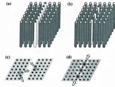
HOTONIC band gap structures provide a promising tool to control of the flow electromagnetic (EM) waves in the integrated optical devices. Therefore, there is a growing interest in developing photonic crystal-based waveguide components which can guide and bend EM waves either along a line defect (a row of missing rods),^®’“*® which is also called planar waveguide (PW ) [See Fig. 3.1(a)] , or through coupled cavities,^® which is known as coupled-cavity waveguide (CC W ) [See Fig. 3.1(b)]. In the former case, the EM waves are conflned in one direction which is perpendicular to axis of missing rods, and photons can propagate in other direction parallel to the axis of the missing rods [Fig. 3.1(c)]. In the latter case, which we named coupled-cavity waveguides (CCW),^® the EM waves are tightly conflned at each defect site, and photons can propagate via hopping due to interaction between the neighboring evanescent cavity modes [Fig. 3.1(d)].By removing or adding materials to a perfect photonic crystal, it is possible to create localized EM modes inside the photonic band gap which are reminiscent of the acceptor and donor impurity states in a s e m i c o n d u c t o r . T h e r e f o r e , photons at certain
CHAPTER 3. PHYSICS AND APPLICATIONS OF CCWs 16 (a) (c) 0 9 0 · © · · · • o · o • ® ® ® © © © · ^[© © o e • · ·. •r->^ «>· ® · © 0 '‘^ © © © © © © © ^ © © © © i © © © ^ © © © © (d) ,: © < /0 0 /© O I ..., I © © O © 0/ © #. © o ©/ » © © · ©y © © © © , O 0 © # ,'o © © /0 © © ||; © © ©/ '*■ • 1 · , I»/ ►0/ V y ’/
Figure 3.1: Schematic drawing of (a) planar and (b) coupled-cavity waveguides in photonic crystals, (c) Planar waveguides (PW ) consist of two parallel photonic crystal mirrors with a suitable separation between them. Photons confined between these two photonic crystal walls, and can propagate through the opening which can be considered a continuous defect, (d) Coupled-cavity waveguides (CC W ) are formed by removing an array of rods (white circles) from a two-dimensional photonic crystal (black circles). Tightly confined cavity mode interacts weakly with the neighboring cavity modes, and therefore the electromagnetic waves can propagate through coupled cavities.
wavelengths can locally be trapped inside the defect volume. This important property can be used in various photonic applications. In fact, most of the aforementioned applications are based on cavity structures built around photonic crystals.
Since most of the photonic crystal based applications have been demonstrated in two-dimensional (2D) photonic structures, especially at optical wavelengths, it is very important to study 2D CCW s in details. In this chapter, we will present a comprehensive experimental and theoretical study on 2D coupled-cavity structures. This chapter is organized as follows: In Sec. 3.1, we present observation of the eigenmode splitting, and comparison of measured results with the TB predictions. In Sec. 3.2, we experimentally demonstrate guiding and bending of EM waves through the CCWs, and numerically obtain the corresponding field patterns. The coupled-cavity based splitting and switching
CHAPTER 3. PHYSICS AND APPLICATIONS OF CCW s 17
Transmitter
Receiver
Figure 3.2: Schematics of the experimental setup for measuring transmission-amplitude and transmission-phase spectra.
structures are investigated in Sec. 3.3.
3.1
Analysis of Localized Coupled-Cavity Modes:
Experiment versus Theory
3.1.1 Experimental Setup
We first construct 2D triangular photonic crystals which consist of dielectric cylindrical alumina rods having radius 1.55 mm and refractive index 3.1 at the microwave frequencies. The lattice constant and the corresponding filling fraction are a = 1.3 cm and T] ~ 0.05, respectively. Length of the rods is 15 cm. The experimental set-up consists of a HP 85IOC network analyzer and microwave horn antennas to measure the transmission-amplitude and the transmission-phase properties (Fig. 3.2). The transverse magnetic (TM ) polarization, the incident electric field was parallel to the rods, is considered in all measurements. It is well known that the other polarization, transverse electric (TE), does not produce any photonic band gaps in this frequency range. ^
CHAPTER 3. PHYSICS AND APPLICATIONS OF CCWs 18
Figure 3.3: [Left panels] Measured (solid lines) and calculated (dotted lines) transmission spectra by using FDTD m ethod’ for (a) a single cavity, (b) two coupled cavity, and (c) three coupled cavity structures. Due to coupling between the strongly localized cavity modes, single cavity mode splits into two or three distinct modes depending on the number of coupled cavities. There is a good agreement between the measured and calculated transmission spectra. [Right panels] Schematics of the corresponding coupled- cavity structures where (o) symbols denote the removed rods.
The transmission spectra and the field patterns are obtained by using a finite- difference-time-domain (FDTD) code. In our experiments, normalization of the transmission and the phase data is done as follows. First, we measured the transmission and phase spectra in the free space (i. e., without photonic crystal). This data was used as the calibration data for the network analyzer. Then, we inserted the crystal between the horn antennas, and we performed the transmission and phase measurements by keeping the distance between transmitter and receiver antennas fixed. In FDTD simulations, we normalized the transmission spectra with respect to the source spectra.
CHAPTER 3. PHYSICS AND APPLICATIONS OF CCW s 19
Measurement FDTD TB TBt Ti 0.869 0.871 0.863 0.866 T2 0.904 0.903 0.908 0.904 T3 0.938 0.940 0.935 0.937
t Second nearest neighbors coupling was included.
Table 3.1: Comparison of the resonant frequencies of three coupled cavities obtained by measurements, the FDTD simulations, and the tight-binding (TB) approximation. The measured results are in excellent agreement with the FDTD simulation results, and the prediction of the TB approximation.
3.1.2
Eigenmode Splitting
The crystal exhibits a photonic band gap extending from O.TScjq to 1.14a;o where cjo = cj2a = 11.54 GHz. Figure 3.3 [left panel] shows the measured and calculated transmission characteristics of various coupled-cavity structures. Corresponding schematic drawing of these structures are displayed in right panel of Fig. 3.3. When we remove a single rod from otherwise perfect crystal, a highly localized cavity mode appears at frequency iio = 0.908 uq having a quality factor of 900 [Fig. 3.3(a)]. Next, we measure and calculate the transmission through a crystal which contains two coupled cavities with an intercavity distance A = \/3a. As shown in Fig. 3.3(b), we observe that the single cavity mode is split into two resonance modes at ui = 0.879 ujo and CJ2 = 0.928 (jjQ due to interaction between two adjacent localized cavity modes.
Localized defect modes in 2D photonic crystals is widely studied in literature,^^'^^ and splitting of eigenmode is already reported in various photonic structures. This phenomena is observed in 3D diamond wire mesh photonic crystals,^^ coupled dielectric s p h e r e s , c o u p l e d pairs of micrometer-sized semiconductor c a v i t i e s , t w o polymer bispheres in c o n t a c t , a n d coupled defects in 3D dielectric photonic crystals.
In the case of three coupled cavities, the eigenmode splits into three resonance frequencies. As shown in Fig. 3.3(c), there is a good agreement between measured
CHAPTER 3. PHYSICS AND APPLICATIONS OF CCW s 20
0.86 0.89 0.92 F re q u e n c y (co/cOq)
0.95
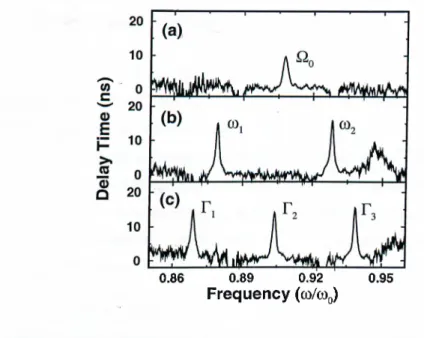
Figure 3.4: Measured delay time characteristics of the corresponding coupled-cavity structures, namely, (a) single cavity, (b) two coupled-cavity, and (c) three coupled-cavity. Tp exhibit peaks at the resonance frequencies which implies that photons spend more time inside the cavities for these frequencies.
and simulated results. We also compare the TB predictions of the resonant frequencies r i,2,3 with the measured and the FDTD simulation results (see Table 1). In order to calculate these frequencies, we first determine the first order TB parameters ai and pi by inserting the measured values of ui and uj2 into Eq. (2.4). Then, Fi^2,3 are obtained by using these parameters in Eq. (2.9) where the second nearest neighbor coupling terms are ignored. As shown in Table 1, the predictions of the TB approximation agree well with the measured and the FDTD results. When the second nearest neighbor coupling terms 0^2 and /^2 * are included into Eq. (2.9), better agreement is obtained, especially for F2.
*These parameters are determined similar to the first order case. Experimental values of cji,2 are obtained by increasing the intercavity distance to 2A.
CHAPTER 3. PHYSICS AND APPLICATIONS OF CCWs 21
3.1.3 Delay Time Measurements
We also measured the delay time corresponding to these coupled-cavity structures. In experiments the delay time Tp is obtained from the phase measurements via Tp = d{A(f)/duj. Here A(p is the net phase difference between the phase of the EM wave propagating through the photonic crystal and the phase of the EM wave propagating in free space. Figure 3.4 displays the measured delay time characteristics as a function of frequencies. Drastic enhancement of Tp at the resonance frequencies implies that the EM waves are confined inside the cavities, and therefore propagate more slowly compared to the free space EM waves.
3.2
Coupled-cavity waveguides (C C W s)
The efficient guiding and bending of light on integrated photonic devices are important to design optical circuits for technological and optical computing applications. Also, the problem of the guiding light around sharp corners must be addressed. Conventional dielectric or metallic waveguides have large scattering losses when sharp bends are introduced. In recent years, it has been demonstrated that photonic crystal based waveguides can efficiently guide and bend EM waves.
3.2.1
Transmission Measurements and FDTD Simulations
In this section, we investigate the transmission and phase properties of straight and zig-zag CCWs in details.
Straight C C W s
We first measure and calculate the transmission spectra of a straight C CW that is formed by removing an array of rods, 10 consecutive defects, along a straight line. The
CHAPTER 3. PHYSICS AND APPLICATIONS OF CCWs 22 0.6 0.8 1.0 Frequency ((o/cOq) 1.2 O O O O O W 0 O O O 01 0 O O O O O 0 O 0 O 1 O C> 0 0 01 O O O Q O oi ; 0 Q 0 0 6 0 O G O O j 0 o o o o ^ o o o o o| 0 0 0 0 OWb 0 O O O i 0 O O 0 0 0 0 G O O i 1 0 O O O 0 . f l | 0 O O 0 0 0 O 0 0 0 ^O 0 0 o o o O O O O Ojg||(^0 O O 0 0 b o O O O O O O o o O O O o 0 0 0 0 o o j b O O O O 0 0 * 0 0 o O oi 1 O O O O O O O O O O i b o o O 0 0 0 0 0 G G G O O 0 O b 0 0 0 0 0 O O 0 O G ^ O 0 G G G O 0 o 0 0 0 ® p 0 O O O G ' 0 O O 0 0 0 % O O G O b : O o o o o|k o G O 0 o ' b ,0, o o, .'0: b.,.0„;0.,„b,.„Gi!
Figure 3.5: [Left Panel] Measured (solid line) and calculated (dotted line) transmission spectra of the straight coupled-cavity waveguide which is generated by removing 10 adjacent rods from the crystal. A cavity band is formed extending from 0.857 ojq to 0.956 ujo- Nearly 100 percent transmission is achieved for certain frequencies. [Right Panel] Calculated field distribution of the C C W for a frequency within the cavity band, namely, u = 0.920 ujo- The guided mode travels along the cavities due to coupling between the localized cavity modes. The electric field E is polarized along the axis of
missing rod. ,
corresponding structure is displayed in right panel of Fig. 3.5 (o symbols). A waveguiding band, or defect band, is formed due to coupling between the evanescent defect modes. Recently, Bayer et al. observed formation of a photonic band due to coupling between the optical molecules.^®
As shown in Fig. 3.5 (left panel) the defect band is extending from 0.857 u>q
to 0.956 u>o· The number of peaks in the transmission spectrum is equal to the number of cavities in the structure as expected. It is also observed that the complete transmission is achieved for certain frequencies within the defect band. Since each mode is strongly localized around the removed rod, and the guided mode is composed of linear combination of these individual defect modes, we expect that the radiation loss mechanism is absent in these structures. We also calculate the corresponding field distribution of the guided mode for u> = 0.920 u>o. Figure 3.5 (right panel) clearly shows that the guided mode is completely confined along with the coupled-cavity array, and
CHAPTER 3. PHYSICS AND APPLICATIONS OF CCWs 23 p"0 O O O O O I 0 0 0 o'q 6 O' O' 0.8 1.0 Frequency (co/cOq) o o o o'0'‘“‘^:”W''0''0'''0'''0:''''0; o o o o o o o o o o ; 0 0 0 0 O ^ 0to o o o o 1 O O O O 0 , 0 O o O J O O O O O <> 0 o d 0 o ^ 0 1 o 0\ 0 o o'' o' 1 o 0 0 <^6 o 0^0 o o 0 o d o o 0 0 o # 0? 0 d O 0 d O O O O O O O : o o o o o o o OiiDi «^0 d o o o o o o o d d o ) O O O o O O ^ p 0, 0 q ' o o o qwP €l o o d d 0 I 0 O Q ^ |B |d O o O O O d 1 o o |B p o ^ o o o o o o 1 o © ofo o o o o O O O d 1 2 o o o o o o o 0 i 0 ^
Figure 3.6: [Left Panel] Measured (solid line) and calculated (dotted line) transmission spectra of the zig-zag coupled-cavity waveguide which contains 16 cavities. [Right Panel] Calculated field distribution of the zig-zag CC W for a frequency within the cavity band, namely, uj = 0.936 uq.
propagates along with the cavity sites.
Z ig -Z a g C C W s
We then measure and calculate the transmission characteristics of a zig-zag waveguide which consists of 16 coupled cavities. The distance between cavities are the same, even if propagation direction is arbitrarily changed. Figure 3.6 (left panel) displays corresponding transmission spectra as a function of normalized frequency. A defect band is formed between 0.857 ujo and 0.949 uq. We also achieve complete transmission for certain frequencies within the defect band. Although the zig-zag CCWs have many sharp corners, these waveguides exhibit properties similar to the straight CCWs.
Based on our observations, the crystal symmetry has a crucial role in 2D photonic crystals to achieve complete transmission of EM waves through CCWs.^^ For instance, even if the triangular symmetry leads nearly full transmissions, one can obtain only 10% transmission for the square photonic c r y s t a l s . W e think that this observation is related with the localization properties of the cavity mode, and the nature of the interaction
CHAPTER 3. PHYSICS AND APPLICATIONS OF CCWS 24
100
kA/n 0.85 Frequency (co/cOg)0.90 0.95
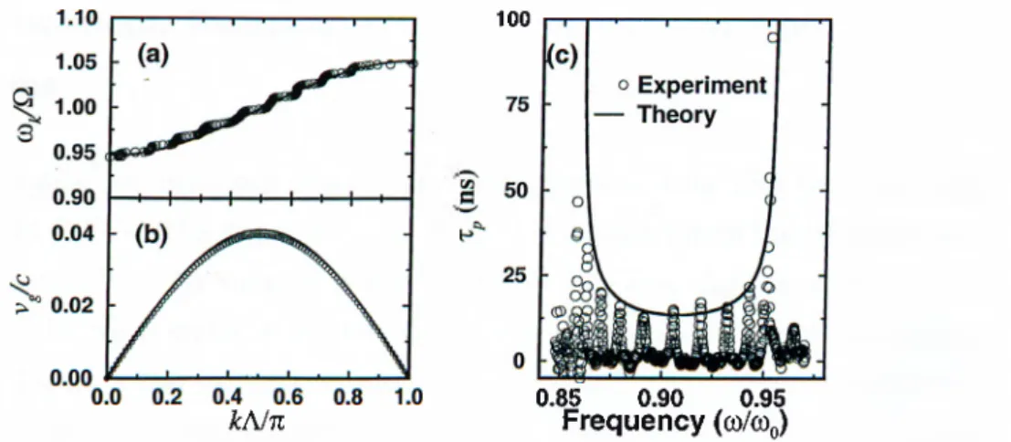
Figure 3.7: Comparison of the measured and calculated (a) dispersion relation, (b) group velocity, and (c) delay time corresponding to the straight CCW . Eqs. (2.16), (2.18), and (2.21) are used to determine oj{k), Vg, and Tp with k = —0.0525, respectively. There is good agreement between the experimental results and the predictions of the tight-binding approximation.
between the cavity modes.
i
It is important to note that the TB parameter ac can also be determined from the bandwidth of the defect band by using \k\ = Ac(;/2fio — 0.054. This result is very close to the previously obtained value in Sec. 3.1.2. In addition, the bandwidth of a C CW band can be adjusted by changing the localization properties of the cavities, or the coupling strength (overlap integral) between the localized cavity modes. For instance, decreasing the intercavity distance leads to a wider bandwidth.
Previously, Scalora et ai have proposed a switching mechanism which can be achieved by dynamical shifting of the photonic band gap edges via the nonlinear p r o c e s s e s . A s shown from Fig. 3.5, the defect band has very sharp band edges compared to the PBG edges, and therefore this property can be used to construct photonic switches by the changing position of the defect band.^®’^°
CHAPTER 3. PHYSICS AND APPLICATIONS OF CCWs 25
3.2.2 Dispersion Relation, Group Velocity, and Photon Life
time
We also determine the dispersion relation, group velocity, and delay time corresponding to the straight CCWs. The dispersion relation u{k) is obtained from the transmission- phase i n f o r m a t i o n . B y measuring the net phase difference A(p, as a function of frequency u>, the wave vector k of the crystal can be determined directly by using Eq. (2.20). Figure 3.7(a) exhibits comparison of measured and calculated dispersion relation as a function of wave vector k. The theoretical curve is obtained by using Eq. (2.16) with experimentally determined TB parameter k = —0.0525. We also plot group velocity of the propagating mode by using Eq. (2.18). The experimental curve is determined from the measured dispersion relation. As shown in Fig. 3.7(b), group velocity vanishes at the defect band edges, and the maximum value of the group velocity is one order of magnitude smaller than the speed of light.
Measured and calculated delay time characteristics of the straight waveguide is displayed in Fig. 3.7(c). The delay time increases drastically at the C C W band edges. This result agrees well with our TB analysis (dotted line). The number of observed peaks in the delay time spectrum is equal to the number of cavities used in the structure. Physically, heavy photon concept in the photonic band gap structures is reminiscent of heavy electron in semiconductors having energies near the band edges. The corresponding eigenfunctions are standing waves rather than the propagating waves, and therefore the effective mass of electrons becomes very large.
3.3
Splitters and Switches
Splitters and switches are important components for the design of photonic circuits. In recent years, several authors reported splitters and switches which are built around photonic band gap s t r u c t u r e s . I n this section, we demonstrate splitting of propagating waves into two output waveguide ports. We also report a switching
CHAPTER 3. PHYSICS AND APPLICATIONS OF CCWs 26 — Experiment — FDTD ____ ____ Ki__ o|||po 0 0 0 0 0 0 ommo0| i 0 O ^ 0 0 0 0 0 0 0 OTO o I 0 o o o o o o o|i|bo oi o O O O O 0 o o o b o O o O O o O 0 :0 O O ; O ; O O O O O O O O O l O O l o 0 -0 O, O O O 0 o o _j,0 b o o 0 O/ ' QaiP O O^ ’ !^, 6 0 0 0 0 ojjHo ouK po' o'oq , 0 0 0 0 0 0 0 0 0 0 O 6 0 0, .0 0 0 0 0 '^ ' O 0 0 0 6% (^b O '0 o o b o o o o 00 o ;o o o o o o o o b 0^0 o o 6 0 o o o o O o o o o o , O 0 O O O Ol(|fo O o 0 0 O p O O O O O Ogb 0 . 0 O 0 0 1 O o o o o o|M O O O O O i b„„O...0!.0..0,Jfii.,. ofo,,..0t,0..0.vi0„.,0:...o!
'o1
0.8 1.0
Frequency (od/cDo)
Figure 3.8: [Left Panel] Measured (solid line) and calculated (dotted line) of transmission spectra of a Y-shaped coupled-cavity based splitter. The electromagnetic power in the input port splits equally into the two output waveguide ports for frequencies throughout the cavity band. [Right Panel] The calculated power distribution inside the input and the output waveguide channels of the splitter for frequency uj = 0.916 uq.
mechanism based on coupled-cavity structures.
In order to demonstrate the splitting of EM power, we construct a Y-shaped splitter which consists of one input CCW and two output CCWs. The input and output waveguide ports contain 5 and 6 coupled cavities, respectively. As shown in Fig. 3.8 (left panel), the propagating mode inside the input C CW splits equally into two output C C W ports for all frequencies within the defect band. We also compute the electric field distribution inside the input and the output CC W channels for frequency cu = 0.916 ouq.
In the present structure, the splitter structure can also be used as a photonic switch. To demonstrate the switching effect, we place a single rod to the left side of junction of Y-splitter. This breaks the symmetry of the structure, and therefore one can regulate the amount of power flow into the output ports of CCWs. As shown in Fig. 3.9, the
CHAPTER 3. PHYSICS AND APPLICATIONS OF CCWs 27 ^ O'TIS 0 o A ‘0 0 0 0 0 0 0 0, f O O O O O O O 0;^ o 0 0 O O O o o o b ; o, o o ■ 6 o o 0..0 ,b p o 0 0 0 0 q 0 o'Á o q.,,0. 6 o'bl'o-'O o ,m r i o 1 6 :o\o. o/p 0^ ” o M W . j 0/ o o q tm o1 I b. o - ’# b ^ p. q: p 9 I Ip o o 0 0 o‘b 0 o 6: 0 0 0 0 0 O' ^ 0 0 O .,0 0 I p O O O O © 0 : 0 O O O b O O O 0 O (^ |H0 0 0 . 0 0 o
b O O O O,. O O^ pop OOP fo O 0 0 O 0 00 0 9 Q o. o. 0 o o -^^W^o o o o o ©:
: o o o o o.<^ «¿0 o 0- 0 o I
Mjt. kHiLJim «(.,».
Figure 3.9: [Left Panel] Measured (solid line) and calculated (dotted line) transmission characteristics of a coupled-cavity switching structure. [Right Panel] Corresponding field pattern clearly indicates that most of the power is coupled to the right port.
power at each output waveguide’ port is drastically changed. While most of the input power for frequencies throughout the defect band is coupled to the right port, only a few percent of the input power is coupled to the left port. The simulated electric field distribution is also displayed in right panel of Fig 3.9.
3.4
Summary
In this chapter, a comprehensive study on the coupled-cavity structures in two- dimensional triangular dielectric photonic crystals have been presented. The phenomena of eigenmode splitting is observed when the isolated localized coupled-cavity modes are brought into contact. A new type of waveguiding mechanism, propagation of photons by hopping, is demonstrated in two-dimensional photonic crystals. Nearly full transmission of electromagnetic waves is achieved even if the coupled-cavity waveguides contain very sharp bends and the propagation direction is arbitrarily changed. Coupled-cavity waveguide structures are also used to design power splitters and photonic switches. These
CHAPTER 3. PHYSICS AND APPLICATIONS OF CCW s 28
results are very important for designing efficient waveguide components in photonic crystal based optical circuits.
Chapter 4
I
nvestigation
of
C
oupled
-C
avities
IN
3D P
hotonic
C
rystals
T
HE ARTIFICIALLY created 3-dimensional (3D) periodic structures inhibit the propagation of electromagnetic (EM) waves in a certain range of frequencies in all d i r e c t i o n s . I n analogy with electronic band gaps in semiconductors, these structures are called photonic band gap (PEG) materials or photonic crystals.^’'* The initial interest in this area came from the proposal to use PEG crystals to control spontaneous emission in photonic devices.^ However, the technological challenges restricted the experimental demonstrations and relevant applications of these crystals to millimeter wave and microwave frequencies.®“’^ Recently, Fleming and Lin reported a photonic crystal with a band gap at optical frequencies.®®’®® With this breakthrough, initially proposed applications like thresholdless semiconductor lasers®^ and single-mode light- emitting diodes®®’®® became feasible.As we explained in previous chapters, by breaking the periodicity of the photonic crystal, it is possible to create highly localized defect modes within the photonic band gap, which are analogous to the localized impurity states in a semiconductor.^^ Photons hop from such a evanescent defect mode to the neighboring one due to overlapping of the tightly confined modes. This is exactly the classical wave analog of tight binding
CHAPTER 4. COUPLED-CAVITIES IN 3D PHOTONIC CRYSTALS 30
(TB) method in solid state p h y s i c s . T h e TB formulation has been proven to be very useful in studying electronic properties of solids.®
In this chapter, we investigate experimentally and theoretically the coupling between localized cavity modes in a dielectric-based layer-by-layer 3D photonic crystal within the TB framework. In Section 4.2, we report on the observation of the eigenmode splitting in the coupled cavities. We demonstrate a new type of waveguiding through localized defect modes in Section 4.3. We analyze the delay time characteristics of single cavity mode and coupled-cavity modes in Section 4.4.
4.1
3D Layer-by-Layer Photonic Crystals
A layer-by-layer dielectric based photonic crystal®®’®^’^® was used to construct the coupled-cavity structures as shown in Fig. 4.1(a). The crystal consists of square shaped alumina rods having a refractive index 3.1 at the microwave frequencies and dimensions 0.32 cmxO.32 cm x 15.25 cm. A center-to-center separation between the rods of 1.12 cm was chosen to yield a dielectric filling ratio of ~ 0.26. The unit cell consists of 4 layers having the symmetry of a face centered tetragonal (fct) crystal structure. The crystal exhibits a three dimensional photonic band gap extending from 10.6 to 12.8 GHz.
The experimental set-up consists of a HP 8510C network analyzer and microwave horn antennas to measure the transmission-amplitude and transmission-phase spectra [Fig. 4.1(b)]. The defects were formed by removing a single rod from each unit cell of the crystal. Removing a single rod from an otherwise perfect crystal leads to confined modes with high Q-factors, quality factor defined as the center frequency divided by the full width at half maximum, around 1000. The electric field polarization vector of the incident EM field was parallel to the rods of the defect lines for all measurements.
CHAPTER 4. COUPLED-CAVITIES IN 3D PHOTONIC CRYSTALS 31
Removed Rods
Figure 4.1: (a) Schematic drawing of the coupled-cavity structures in a layer-by-layer photonic crystal. A single rod (white rods) removed from each unit cell, (b) The experimental setup for measuring the transmission characteristics of the coupled-cavity structures in three-dimensional photonic crystals. The electric field polarization is directed along the removed rods.
4.2
M ode Splitting
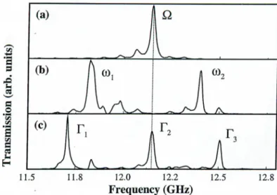
By using the aforementioned experimental setup, we first measured the transmission amplitude through a crystal with a single defective unit cell. This resulted in a localized defect mode within the PBG which is analogous to acceptor impurity state in semiconductor p h y s i c s . T h e defect mode occurred at a resonance frequency of ii = 12.150 GHz with a Q-factor (quality factor, defined as center frequency divided by the peak’s full width at half-maximum) of ~ 1000 [Fig. 4.2(a)].
Next, we measured the transmission through the crystal that contains two consecutive single rod removed unit cells. The intercavity distance for this structure was A = 1.28 cm, which corresponds to single unit cell thickness in the stacking direction. We observed that the mode in the previous case splitted into two resonance modes at frequencies u>i = 11.831 GHz and uji = 12.402 GHz [Fig. 4.2(b)]. The TB parameters found to be /i = /? - a = -0.047.
Figure 4.2(c) shows the transmission characteristics of a crystal having three consecutive defective cells, where the resonant modes were observed at frequencies Fi = 11.708 GHz, Fa = 12.153 GHz and Fg = 12.506 GHz.
CHAPTER 4. COUPLED-CAVITIES IN 3D PHOTONIC CRYSTALS 32
Figure 4.2: Transmission characteristics along the stacking direction of the photonic crystal: (a) For single defect with resonance frequency ii. (b) For two consecutive defects resulting in two splitted modes at resonance frequencies u>i and u>2 with intercavity distance A = 1.28 cm. (c) For three consecutive defects with resonance frequencies Fi, F2, and Fa.
Measured [GHz] Calculated [GHz]
El 11.708 11.673
E2 12.153 12.150
E3 12.506 12.492
Table 4.1: The measured and calculated values of resonant frequencies for the crystal with three defective unit cells.
Table 4.1 compares the resonance frequencies, which were calculated by inserting TB parameters cci and /?i into the Eq. (2.9), with the values obtained from the experiment [Fig. 4.2(c)]. The experimentally measured three splitted modes coincide well with the theoretically expected values. This excellent agreement shows that the classical wave analog of TB formalism is valid for our structure.
We have observed the splitting phenomena by using laser-micromachined alumina (W-band, 75-120 GHz) photonic crystals.®^ As shown in Fig. 4.3, the single cavity mode splits into two distinct modes. The TB parameter aci = —0.045 was found to be
![Figure 3.3: [Left panels] Measured (solid lines) and calculated (dotted lines) transmission spectra by using FDTD m ethod’ for (a) a single cavity, (b) two coupled cavity, and (c) three coupled cavity structures](https://thumb-eu.123doks.com/thumbv2/9libnet/5948784.124034/35.1002.273.690.257.600/figure-measured-calculated-transmission-spectra-coupled-coupled-structures.webp)
![Figure 3.8: [Left Panel] Measured (solid line) and calculated (dotted line) of transmission spectra of a Y-shaped coupled-cavity based splitter](https://thumb-eu.123doks.com/thumbv2/9libnet/5948784.124034/43.1002.273.791.254.603/figure-panel-measured-calculated-transmission-spectra-coupled-splitter.webp)
![Figure 3.9: [Left Panel] Measured (solid line) and calculated (dotted line) transmission characteristics of a coupled-cavity switching structure](https://thumb-eu.123doks.com/thumbv2/9libnet/5948784.124034/44.1002.277.753.237.551/figure-measured-calculated-transmission-characteristics-coupled-switching-structure.webp)