A Performance Enhanced Power Divider Structure
Vahdettin Tas1,2, Abdullah Atalar1
IDepartment of Electrical and Electronics Engineering, Bilkent University, Ankara, Turkey 2Power Amplifier Technologies Divison, REWIS, Aselsan Inc., Ankara, Turkey
vtas
@
ee.bilkent.edu.tr, aatalar@
bilkent.edu.trAbstract-We analyze the bandwidth capability of a divider with a series RLC circuit at the isolation arm. Analytical expressions for optimal component values are given. Bandwidth limiting effect of the pad capacitances of the chip resistors is analyzed. These parasitic capacitors are compensated by the proposed structure. Broadband characteristic of the new divider is verified by experimental results.
Index Terms-wideband power divider, isolation resistor par asitics, pad capacitance.
I. INTRODUCTION
Power dividers are used at microwave frequencies to direct the power to two or more loads with minimal loss. The Wilkinson power divider was introduced in 1960 [1]. It is matched at all ports and has good isolation between the output ports within a frequency band. Cohn [2] introduced the multi section hybrids to overcome the bandwidth deficiency of the Wilkinson dividers. Broadband power division using multisection structures was revealed in several works [3], [4]. RLC networks in series or parallel configuration have been used to design dividers for dual band operation [5], [6], [7]. In these studies, a detailed analysis for broadband operation is not available. In [8], wideband isolation characteristic was analyzed using series RLC network but the final design lacks a good input return loss and insertion loss characteristic.
In this work, the divider with a series RLC network in the isolation arm is analyzed with a special focus on the tradeoff between bandwidth and desired S-parameter level of the isolation and input-output return losses. Analytic expressions for the required component values are derived. Bandwidth limiting effects of the parasitics of the isolation resistor is discussed. A divider structure is designed to eliminate the dominant parasitic effects.
II. ANALYSIS AND DESIGN OF THE DIVIDER
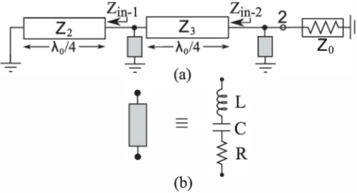
In Fig. 1, a symmetrical multisection 2-way divider network is depicted. The network is composed of loss less quarter-wave transmission lines apart from the isolation arms shown with gray boxes. For a classical multisection Wilkinson divider, the gray boxes are composed solely of the isolation resistors.
Inclusion of reactive elements in the gray box in addition to the resistor can increase the bandwidth performance of the divider considerably. Fig. 2-a illustrates the odd mode equivalent circuit of the divider in Fig. 1. The transmission lines are quarter wavelength at the center frequency of fa.
Zin-l
is inductive for f < fa and capacitive for f > fa.This I imits the bandwidth of the divider. For compensation, a
Fig. I. A symmetrical 2-way power combiner/divider network. White boxes are quarter-wave transmission lines. Gray boxes represent the lossy isolation arms. Possible contents of a gray box: Symmetrical loss less components with isolation resistors in the middle.
�I
Zo
(b)
Fig. 2. a) Odd mode equivalent circuit of the divider in Fig I. b) Possible content of a gray box for wideband operation: Series RLC network.
resonator with the opposite characteristic is required. A series RLC network shown in Fig. 2-b is suitable for this purpose.
Fig. 3-a shows the overall structure for the two-section case. Even mode tuning element is a transmission line and odd mode tuning element is a series LC circuit. To preserve the symmetry, capacitors and inductors are placed at two sides of the resistor. We analyze the trade off between bandwidth and the S-parameter levels. The even mode equivalent circuit is illustrated in Fig. 3-b. To maximize the bandwidth of the impedance conversion from
Zo
to2Zo,
the parameters2Z1
andZ2
are chosen to satisfy the following equation [9]:2Z1Z2
=2Zg
(1)By allowing a nonzero reflection coefficient
Ifel
<0 (0
«1),
the bandwidth of operation can be extended. At the band center, fa, we have:Z? 2Zo
_Z 1
+f e
4Zf - 01_ fe
(2)With the condition
f e
=0
at fa (reducing the impedanceconversion ratio), (2) can be rewritten as:
Zl
�
1 1 - 0/2
Z2
=V
2(1+5)
�y'2( 1
+0/2)
(3)
Using (1) and (3),
Zl
andZ2
are calculated as:Zl
=T1/4(1_ 0/2)
Zo
Z2
=21/4(1 + 0/2)
Zo
(4) (5) The odd mode equivalent circuit is shown in Fig. 3-c. L/2
2Z, Z, Cr
�7.
!
2Z o o . , .!�
(b) Z, Cr�
-:!:- "
-:- .I
t��
R/2 Zi
-:-(c)-:-Fig. 3. a) Broadband 2-way divider. b) Even-mode equivalent circuit. c) Odd-mode equivalent circuit.
and 2C resonate at the band center:
1
!T'r1 =
27r fo
yLC (6)
At
fo,
we imposeIfol
= o. So,R
can take two values:R
=2Zo(1
±0)/(1
=t=0).
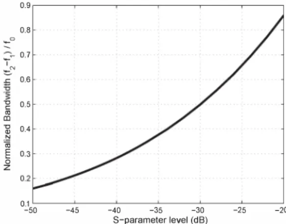
The smaller one results in a wider band, since the resistive component gets dominant with respect to the shorted transmission line. So, we find0.9 0.8 _0 -� 0.7 , ,,=-N .<:: 0.6 '5 ;: " 0.5 c: '" co " 0.4 Q) .!:! (ij E 0.3 0 z 0.1 -50 '---�--�--�-�--�---' -45 -40 -35 -30 -25 -20 S-parameter level (dB)
Fig. 4. Achievable bandwidth versus the desired S-parameter level for the divider in Fig. 3. The bandwidth is normalized with the center frequency.
2 .,.,., 1.8 � 1.6 c: '" � ""'" Z,/Zo(O) , • , • , R,IZo (0)
§"'.4
�r---�
__ .t::! 1.2 IIIII111111111111I11111111111111111 (ij E � 1 0.8 •••••••••••••••••••••••••• -50 -45 -40 -35 -30 S-parameter level (dB) -25 -20R
1 - 0
- =2
-;::;:; 2(1 - 20)
Zo
1 +0
(7) Fig. 5. The component values to achieve the bandwidth ranges expressed in Fig. 4.To calculate L and C analytically, we follow the approach in [2]. We define the bandwidth condition of
If
eI
<0
asfo(1 - k)
<f
<fo(1 + k).
SinceZl
andZ2
are calculated using (4) and (5),k
is a known parameter. To maximize the overall bandwidth, we assume that theIfol
<0
condition covers the same frequency range and calculate L aswhere
woL
Zo
(1 - k)(b + v'b2 - 4ac)
ak(2 - k)
(8)a
=1 + evl2(1 + 0) ) b
=25/4t(1 + 0/2)
(9)c
=1 - 40 ) t
=tan(7r/2 - k7r/2)
(10)Fig. 4 shows the bandwidth performance of the divider. Between the frequencies hand 12, the parameters
IS11 I,
IS221, IS321
stay below the prescribed S-parameter level. Fig. 5 is a plot of the required component values to achieve the bandwidth ranges expressed in Fig. 4.The implementation of this circuit is difficult due to the parasitics of the lumped components. Even the small pad capacitors to ground of the serial components significantly affect the performance. Fig. 6 shows a high frequency model of a chip resistor. For the even mode, the components
R,
L s, Csare not in the picture, but the pad capacitance Cp results in a path to the ground which degrades the bandwidth performance of the divider. To prevent this, Cp should be tuned out. For this purpose, we propose the structure in Fig. 7 where Cp is tune
q
out using a shorted transmission line,Zp.
The inductor, L, is implemented with a high impedance transmission line,Zs
that also compensates the parasitics of the capacitor, C. The new configuration of the isolation arm affects also the even mode circuit. The insertion loss due to the resistor is avoided by placing it at the mid point. Being effective also in the even mode, the network in the isolation arm is optimized to enhance the bandwidth of the input return loss as well as the output return loss and isolation. This extra degree of freedom allows the input transmission line,Zl,
to be eliminated. Analysis of these results will be presented in an extended version of this paper.III. EXPERIMENTAL RESULTS
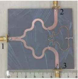
The divider structure introduced in Fig. 7 was implemented on an AD250 substrate with a thickness of 1.6mm. Fig. 8 shows the photo of the divider. It was designed to achieve over
Fig. 6. Equivalent circuit of a chip resistor. 1 Zp R Ep
I·
HI'
Cp cpHI'
I·
Fig. 7. Schematic diagram of a 2-way divider with symmetric transmission lines in the isolation arm to enhance the band and to compensate the parasitics of the resistor.25dB isolation and return loss in the band of 675-1325MHz. Figs. 9 and 10 show the measured results. Return loss values are better that 18.5dB in a bandwidth of 625-1500MHz. In a wider band the isolation is over 20dB. Extra insertion loss is lower than O.2dB and the amplitude mismatch between the output ports is lower than O.ldB.
Fig. 8. Implemented 2-way power divider (Fig. 7).
IV. CONCLUSIONS
A series RLC circuit is utilized in the isolation arm of a Wilkinson divider to improve its bandwidth. Parasitic shunt capacitances of the isolation resistors affect the performance negatively. This effect is eliminated using a new power divider
30 co :3- 20 c 0 � 0 10 .!!1 1:) c ro c ::;
&
-20 -30 0.5 0.75 1 1.25 Frequency (GHz) " , "" dB(S22) , - , - , dB(S33) - - - -dB(S32) 1.5Fig. 9. Measured return loss and isolation characteristic of the divider in Fig. 8. -3�----�---�----��====�� co :3- -3.1 (/) (/) .3 c o t Q) � -3.2 -3.3 '---�----'---�---��"--" 0.5 0.75 1 1.25 1.5 Frequency (GHz)
Fig. 10. Measured insertion loss characteristic of the divider in Fig. 8.
structure. Bandwidth response of the divider is promising for wide band applications.
REFERENCES
[I] E. Wilkinson, "An N-way hybrid power divider," IRE Trans. on Microwave Theory and Techniques, vol. 8, no. I, pp. 116--118, 1960. [2] S. Cohn, "A class of broadband three-port TEM-mode hybrids," IEEE
Trans. on Microwave Theory and Techniques, vol. 19, no. 2, pp. 110-116, Feb. 1968.
[3] H. Oraizi and A.-R. Sharifi, "Design and optimization of broadband asymmetrical multi section Wilkinson power divider," IEEE Trans. on Microwave Theory and Techniques, vol. 54, no. 5, pp. 2220-2231, May 2006.
[4] J-c. Chieh and A.-V. Pham, "Development of a broadband Wilkinson power combiner on liquid crystal polymer," in Microwave Conference, 2009. APMC 2009. Asia Pacific, 2009, pp. 2068-2071.
[5] T. Kawai, 1. Yamasaki, Y. Kokubo, and I. Ohta, "A design method of dual-frequency Wilkinson power divider," in Asia-Pacific Microwave Conference, 2006, pp. 913-916.
[6] X. Wang and I. Sakagami, "Generalized dual-frequency Wilkinson power dividers with a series/parallel ric circuit," in Proc. of 20 I I IEEE MTT-S International, 2011, pp. 1-4.
[7] Y. Wu, Y. Liu, and S. Li, "Unequal dual-frequency Wilkinson power divider including series resistor-inductor-capacitor isolation structure," lET Microwaves, Antennas Propagation, vol. 3, no. 7, pp. 1079-1085, 2009.
[8] J.-c. Kao, Z.-M. Tsai, K.-Y. Lin, and H. Wang, "A modified Wilkinson power divider with isolation bandwidth improvement," IEEE Trans. on Microwave Theory and Technigues, vol. 60, no. 9, pp. 2768-2780, 2012. [9] S. B. Cohn, "Optimum design of stepped transmission-line transformers," IRE Transactions on Microwave Theory and Technigues, vol. 3, no. 3, pp. 16-20, 1955.