GaN/AlGaN-BASED UV
PHOTODETECTORS WITH
PERFORMANCES EXCEEDING THE PMTS
A DISSERTATION
SUBMITTED TO THE DEPARTMENT OF PHYSICS AND THE INSTITUTE OF ENGINEERING AND SCIENCES
OF BILKENT UNIVERSITY
IN PARTIAL FULLFILMENT OF THE REQUIREMENTS FOR THE DEGREE OF
DOCTOR OF PHILOSOPHY
By
Turgut Tut
September 2008
ii
I certify that I have read this thesis and that in my opinion it is fully adequate, in scope and in quality, as a dissertation for the degree of Doctor of Philosophy.
Prof. Dr. Ekmel Özbay (Supervisor)
I certify that I have read this thesis and that in my opinion it is fully adequate, in scope and in quality, as a dissertation for the degree of Doctor of Philosophy
Assist. Prof. Hilmi Volkan Demir (E.E.E.)
I certify that I have read this thesis and that in my opinion it is fully adequate, in scope and in quality, as a dissertation for the degree of Doctor of Philosophy.
Assist. Prof. Ceyhun Bulutay
I certify that I have read this thesis and that in my opinion it is fully adequate, in scope and in quality, as a dissertation for the degree of Doctor of Philosophy.
iii
I certify that I have read this thesis and that in my opinion it is fully adequate, in scope and in quality, as a dissertation for the degree of Doctor of Philosophy
Prof. Dr. Süleyman Özçelik
Approved for the Institute of Engineering and Sciences:
Prof. Mehmet B. Baray
iv
ABSTRACT
GaN/AlG
aN-BASED UV PHOTODETECTORS WITH
PERFORMANCES EXCEEDING THE PMTS
Turgut Tut Ph.D. in Physics
Supervisor: Prof. Dr. Ekmel Ozbay
Sepptember 2008
The recent developments in high Al-content AlxGa1−xN material growth technology made it possible to fabricate high performance solar-blind photodetectors operating in the ultraviolet (UV) spectral region with improved receiver sensitivity, low noise, low dark current density, and high speed. AlGaN-based Schottky, p-i-n, and metal-semiconductor-metal photodetectors (MSM) with very high performances have already been demonstrated.The UV-filtering nature of the atmospheric ozone molecules blocks the solar radiation to reach the earth’s surface for wavelengths shorter than 280 nm. In this case, UV photodetectors with cutoff wavelengths around 280 nm, which are also called solarblind detectors, can detect very weak UV signals under intense background radiation. These devices have important applications including missile plume detection, chemical/biological agent sensing, flame alarms, covert space-to-space and submarine communications, ozone-layer monitoring, and gas detection. Due to their high responsivity (600 A/W), high speed, high cathode gain (on the order of a million), and low dark current properties, photomultiplier tubes (PMTs) are frequently used in such applications. However, PMTs are very expensive and bulky. Besides, they require a cooling system, and they have high operation voltages in excess of 1000 V. To achieve solar-blind detection, PMTs should also be integrated with complex and expensive filters. In order to avoid these disadvantages, high performance solid-state UV photodetectors with high
v
internal gain are needed.Wide band-gap semiconductor photodetectors, such as AlxGa1−xN with x=0.4, are ideal candidates for this purpose. These devices are
intrinsically solar blind, in which no additional filters are needed, they have low noise,and fast response times.The lack of high internal gain has been the major limitation for the usage of AlGaN photodetectors for applications that require high sensitivity detectors. There have been several theoretical research works that examined the avalanche effect in GaN and AlGaN-based structures. However, reproducible high gain in AlGaN-based APDs is still a major limitation. We have designed, fabricated, GaN/AlGaN based photodetectors, and according to characterization measurements, the Schottky, p-i-n, and avalanche detectors have high performance in terms of quantum efficiency, dark current, detectivity, high speed response, and high reproducible avalanche gain.
Keywords: Photodetectors, AlGaN, GaN, Avalanche, high gain.
vi
ÖZET
PMT PERFORMANSINI GEÇEN GaN/AlGaN-TABANLI
UV FOTODEDEKTÖRLER
Turgut Tut Fızık Doktora
Tez Yöneticisi : Prof. Dr. Ekmel Özbay
Eylül 2008
Yakın zamandaki yüksek oranda Al ihtiva eden AlxGa1−xN materyal büyütme teknolojisi ışığın ultraviole dalga boylarında çalışan iyileştirilmiş sensitivite, düşük gürültülü, düşük karanlık akım yoğunluğuna sahip, yuksek hızlı AlGaN tabanlı yüksek performanslı Schottky, p-i-n, ve (metal-yarıiletken-metal) MSM, tipi fotodetektörleri üretmeyi mümkün kılmıştır ve bu tür detektörler imal edilmiştir. Atmosferdeki ozon moleküllerinin ultraviole ışığı 280 nm dalga boyundan küçük değerler için filtrelemesi sayesinde bu dalga boylarındaki güneşten gelen radyasyon dünya yüzeyine ulaşmasını engeller. Bu durum sayesinde, 280 nm civarındaki dalga boyuna sahip kırılma dalga boyundaki UV fotodedektörler ki güneş-körü dedektörler olarak da adlandırılırlar, çok zayıf UV sinyalleri bile algılayabilirler. Bu aygıtlar misil füze uyarı sistemleri, kimyasal/biyolojik ajan tanıma, yangın alarmları, uzay ve denizaltı haberleşmesi, ozon tabakasının durumunu kontrol etme, gaz algılama gibi önemli uygulama alanlarına sahiptirler. Yüksek responsiviteye sahip olması hasebiyle (600 A/W), yüksek hızlı, yüksek katod verimine sahip (milyon mertebesinde), ve düşük karanlık akımlı, foton yükseltici tüpler (FYT’ler) bu tür uygulamalar için kullanılmaktaydı. Fakat, FYT’ler pahalı ve hantal yapıdadırlar. Ayrıca bunun yanında, çalışmak için soğutucu bir sisteme ve çok yüksek voltajlara (1000V) ihtiyaç duyarlar. Ayrıca bu aygıtlar güneş-körü algılama yapabilmek için kompleks ve pahalı filtrelerle beraber kullanılırlar. Bu
vii
dezavanlatajlardan sakınmak için bunların yerine yüksek performanslı yarıiletken dedektörler kullanılmalıdır. Geniş bantlı yarı iletken olan AlxGa1−xN
(x=0.4) tabanlı fotodedektörler bunun için ideal adaylardırlar. Bu aygıtlar yapısı itibariyle güneş körüdürler bu nedenle filtreye ihtiyaç duymazlar, düşük gürültüye ve hızlı fotocevaba sahiptirler. Bu dedektörlerin önündeki en büyük engel ise bu dedektörler çok yüksek içsel kazanca sahip değildirler. Şimdiye kadar bir kaç gurup GaN ve AlGaN tabanlı dedektörlerdeki çığ etkisini teorik olarak incelemişlerdir. Lakin, tekrarlanabilir yüksek kazançlı cığ etkisi ile çalışan fotodedektör üretmek hala çok zordur. Biz gurup olarak kuvantum verimi, karanlık akım, dedektivite, yüksek hız, yüksek tekrarlanabilir çığ verimi açısından yüksek performansa sahip Schottky, p-i-n, ve çığ etkili dedektörleri dizayn ettik, urettik ve karakterızasyonunu yaptık.
Anahtar Kelimeler: Fotodedektörler, AlGaN, GaN, Avalanş (çığ etkisi), yüksek
ix
Acknowledgements
I would like to express my deepest gratitude to my supervisor Prof. Ekmel Ozbay for his invaluable guidance, motivation, encouragement, confidence, understanding, and endless support. It has been an honor for me to work with him, and I learned a lot from his superior academic personality.
I also thank the members of the thesis committee, Asst. Prof. Ali Kemal Okyay, Asst. Prof. Ceyhun Bulutay, Assoc. Prof. Oğuz Gülseren, Prof.Dr. Süleyman Özçelik for their useful comments and suggestions.
I would like to thank all the former and present members of Advanced Research Laboratory for their continuous support. Thank you all, members of the Physics and EE Engineering department for making life easier and enjoyable. I want to especially thank the group members of the detector research team: Necmi Bıyıklı, Mutlu Gökkavas, Bayram Bütün, Serkan Bütün, Tolga Kartaloğlu, İbrahim Kimukin, Erkin Ülker, Tolga Yelboğan. Without them, this work would not be complete. It was a pleasure to work with these hard-working people in the same group. I also want to thank to Murat Güre and Ergün Kahraman for their technical help and keeping our laboratory in good condition.
I would like to thank Mehmet Bayındır, Aşkın Kocabaş, Coşkun Kocabaş, Sinem Binicioğlu Çetiner, Ender Çetiner, Onur Kılıç, Muhammed Acar, Özgür Kelekçi , Kamil Boratay Alıcı, Kaan Güven for their company, moral support and help during my graduate study.
Finally I would like to express my endless thank to my family for their understanding and continuous moral support.
xi
Table of Contents
ACKNOWLEDGEMENTS…..….……….……IX
1.INTRODUCTION………..……….……….…...1
2.THEORETICAL BEACKGROUND…..…..………..…..…..3
2.1 Photodiode Operation
2.2 Optical Design Using TMM Code
3. FABRICATION AND CHARACTERIZATION………...24
4. RESEARCH ON GAN/ALGAN PHOTODETECTORS….…...31
5. CONCLUSIONS AND SUGGESTIONS FOR FURTHER
xii
List of Figures
Figure 2.1.1-Energy band diagram of a Schottky contact………..….5
Figure 2.1.2-
Time dependence waveform of the induced current....8
Figure 2.1.3-
Expected waveform of output current of a photodiode
where hole drift velocity is smaller than electron drift velocity…...9
Figure 2.1.4- Schematics of a p-i-n photodiode…...………...….10
Figure 2.1.5-
Reach-through p+-π-p-n+ APD structure. The π region
is very lightly doped p- type material.The p + and n + regions are
heavily doped………..………..11
Figure 2.1.6-
Constancy of the sum of the electron and hole current
densities across a plane at any x. By way of illustration, four impact
ionizations and five electrons-plus-holes crossing every plane are
illustrated………...……….….….12
Figure 2.1.7-
Growth of the gain G with multiplication-layer width
for several values of the ionization ratio k, assuming pure electron
injection………..…..14
Figure 2.2.1-
Reflection and transmission of an electromagnetic wave
incident on a dielectric film of thickness d2………....….17
Figure 2.2.2-
Reflectivity of 8 pairs of DBR on GaAs substrate…..23
Figure 4.1.1-
Dark current of a 30lm diameter solar-blind AlGaN
photodiode. The inset shows the same plot in logarithmic scale….33
Figure 4.1.2-
I
–V curves of AlGaN Schottky detectors with different
xiii
Figure 4.1.3-(a) Measured spectral responsivity curves as a function
of reverse bias voltage, (b) corresponding spectral quantum
efficiency of Schottky photodiodes……….35
Figure 4.1.4-
(a) Linear plot of I–V data and exponential fit for a
30m diameter AlGaN detector, (b) calculated differential resistance
for the same device……….………...….….37
Figure 4.1.5- (a) High-speed pulse response of a 30µm diameter
device as a function of applied reverse bias, (b) corresponding FFT
curves of the temporal data……….……….….41
Figure 4.1.6-
Second-order exponential fitting to the decay part of
pulse response obtained with (a) 30 µm diameter device, (b) 60 µm
diameter device. ………..…...……..………....42
Figure 4.2.1- Current voltage measurements of a photodetector with
a 200 µm diameter. ………..…....45
Figure 4.2.2-
Responsivity of a 100 µm diameter photodetector for
different reverse bias voltages. ………..….…46
Figure 4.2.3-
Voltage dependence of the quantum efficiency and
capacitance for 100 µm diode………..……..…..47
Figure 4.2.4-Spectral quantum efficiency of the photodetector after
0, 20, and 40 nm recess etch of the top dielectric film. ……...…... 48
Figure 4.2.5 Temporal pulse response of the 100 µm micron
diameter p-i-n photodiodes under 5 V reverse bias voltage and the
corresponding frequency response (inset). ………..49
Figure 4.3.1-
Dark current of a 60 µm diameter photodetector……52
xiv
Figure 4.3.2-
(a) Dark current and photocurrent measurement of a
100 micron diameter photodetector. (b) Corresponding avalanche
gain of the same device. ………...54
Figure 4.3.3- (a) Quantum efficiency measurements of a 100 µm
diameter photodetector. (b) Responsivity measurement of the same
device in a semilog scale. ………....55
Figure 4.3.4- Spectral noise measurement of a high-leakage 100 µm
diameter photodetector with a varying applied reverse bias. …..…56
Figure 4.4.1-
Dark current of a 40 µm diameter photodetector...…59
Figure 4.4.2-
Quantum efficiency with back illumination, in which
the inset shows the results for front illumination. ………...…60
Figure 4.4.3- Mn and Mp as a function of reverse bias voltage …..61
Figure 4.4.4-
Electron and hole impact ionization coefficients in
Al0.4Ga0.6N. ………...………62
Figure 4.5.1-
Dark current measurement data from a 40 µm diameter
photodetector device………...…………..64
Figure 4.5.2-(a) Transmission data from a double side polished
wafer which is used in the fabrication……….……….65
Figure 4.5.2-(b) Responsivity measurements result from a 150 µm
diameter device. ……….………….……….66
Figure 4.5.3-
(a) Gain measurements for a 40 µm diameter device.
(b) Avalanche gain extracted from the photocurrent
measurements………...68
Figure 4.5.4-Dark current measurement data with varying
temperatures……….70
xv
List of Tables
Table 4.1 Bias dependent high-speed characteristics of AlGaN Schottky
photodiodes………42.
Table 4.2 Device area dependen high-speed characteristics of AlGaN Schottky
photodiodes………....43.
1
Chapter 1
Introduction
The recent developments in high Al-content AlxGa1−xN material growth
technology made it possible to fabricate high performance solar-blind photodetectors operating in the ultraviolet (UV) spectral region with improved receiver sensitivity, low noise, low dark current density, and high speedAlGaN based Schottky [1,2], p-i-n [3,4], and metal-semiconductor-metal photodetectors [5] with very high performances have already been demonstrated. The UV-filtering nature of the atmospheric ozone molecules blocks the solar radiation to reach the earth’s surface for wavelengths shorter than 280 nm. In this case, UV photodetectors with cutoff wavelengths around 280 nm, which are also called solar-blind detectors, can detect very weak UV signals under intense background radiation. These devices have important applications including missile plume detection, chemical/ biological agent sensing, flame alarms, covert space-to-space and submarine communications, ozone-layer monitoring, and gas detection. Due to their high responsivity (600 A/W), high speed, high cathode gain (on the order of a million), and low dark current properties, photomultiplier tubes (PMTs) are frequently used in such applications. However, PMTs are very expensive and bulky. Besides, they require a cooling
2
system, and they have high operation voltages in excess of 1000 V. To achieve solar-blind detection, PMTs should also be integrated with complex and expensive filters. In order to avoid these disadvantages, high performance solid-state UV photodetectors with high internal gain are needed [6,7].Wide band-gap semiconductor photodetectors, such as AlxGa1−xN with x=0.4, are ideal
candidates for this purpose. These devices are intrinsically solar blind, in which no additional filters are needed, they have low noise[8], and fast response times[9]. The lack of high internal gain has been the major limitation for the usage of AlGaN photodetectors for applications that require high sensitivity detectors. There have been several theoretical research work that examined the avalanche effect in GaN and AlGaN-based structures [10,11,12]. Experimental work on both GaN [ 13,14, 15,16,17,18,19] and AlGaNbased [20,21,22] avalanche photodiodes (APDs) were also reported. We have designed, fabricated, and according to characterization measurements, the Schottky, p-i-n, and avalanche detectors have high performance in terms of quantum efficiency, dark current, detectivity, high speed response, and high reproducible avalanche gain.
3
Chapter 2
THEORETICAL BACKROUND
This chapter gives a brief explanation to the basic operation principles of a photodetector especially APDs and the design basics for the optical simulations. We will first explain the theoretical background for a p-n junction, Schottky diode, and p-i-n diodes. Also the criteria for a good photodiode are discussed namely quantum efficiency and bandwidth.
Photodetectors can be separated into two classes: quantum detectors and thermal detectors. Thermal detectors respond to heating caused by absorption of the incident radiation. The first requirement for thermal detectors is that the heating effect results in a temperature change. Also, this temperature change should yield a measurable change in a physical parameter such as resistance, capacitance etc. Thermopile, bolometer, pyroelectric, golay cell, superconductor detectors are examples of thermal detectors. Thermal detectors can operate in a very broad spectral range. However, their bandwidth and sensitivity performances are relatively poor. The operation of quantum detectors is based on the photo-effect, in which the absorption of photons by some materials results in an
4
electronic transition to a higher energy level and the generation of mobile charge carriers. Under the effect of an electric field these carriers move and produce a measurable electric current. Photoemissive, photoconductive, and photovoltaic detectors are in this category. They have limited spectral response, but demonstrate high sensitivity and high speed which are very important for optical communication systems. In photoconductive detectors, when photons are absorbed by a semiconductor material, mobile charge carriers are generated (an electron-hole pair for every absorbed photon). The electrical conductivity of the material increases in proportion to the photon flux. An electric field applied to the material by an external voltage source causes the electrons and holes to be transported. This results in a measurable electric current in the circuit. As with photoconductive detectors, photovoltaic detectors are also known as photodiodes rely on photo-generated charge carriers for their operation. A photodiode is simply a n junction whose reverse current increases when it absorbs photons. p-n, p-i-p-n, schottky photodiodes, avalanche photodiodes (APD) are widely used photodetectors. When we apply a reverse bias high enough across a p-n junction, due to high electric field in the depletion region on the order of 106V/cm can
cause electrons to impact-ionize and this results in avalanche gain. Avalanche photodiodes can be used instead of photomultiplier tubes in photon counting applications. Operating principles of schottky and p-i-n photodiodes are discussed in the following sections.
2.1 Photodiode operation
When light incident on a junction of a photodiode, photons having energy larger than or equal to bandgap energy of the semiconductor are absorbed and excess electron-hole pairs are created and then separated by the established electric field in the depletion region. Once the photodiode is connected through an external load in a circuit, a measurable current flows through the circuit which is proportional to the number of photons absorbed and the photo-generated carriers.
5
Schottky photodiodes
The theory of rectification in metal-semiconductor junction was developed in 1930 by W. Schottky who attributed rectification to a space-charge layer in the semiconductor. A schottky barrier is composed of metal and semiconductor which is brought into intimate contact. When metal is deposited on a semiconductor in the thermal equilibrium, the Fermi levels of the two materials must be coincident. The energy band diagram can be seen in Figure 2.1.
The work function is the energy difference between the vacuum level and the Fermi level. This quantity is denoted by qφm for the metal and equal to q(χ+ V
n) for the semiconductor. The potential difference between the metal and the
semiconductor work functions is called the contact potential. qφBn is called the barrier height and is equal to q(φm -χ). Under the abrupt junction approximation that ρ≈qND for x < W , 2 ( ) D W Vbi V qN
Figure2.1.1 Energy band diagram of a Schottky contact
Here ε is the dielectric constant of the semiconductor, ND is the ionized donor
6
applied potential to the junction. The current transport in the metal- semiconductor contacts is mainly due to majority carriers, in contrast to p-n junctions. There are mainly four different transport mechanisms: thermionic emission over the barrier, tunneling through the barrier, carrier recombination or generation in the depletion region, carrier recombination in the neutral region of the semiconductor. Thermionic emission is the dominant transport mechanism, which gives rise to the ideal diode characteristics. Thermionic emission theory is derived by Bethe for high-mobility semiconductors, and diffusion theory is derived by Schottky for low-mobiliy semiconductors. Finally, a synthesis of the two approaches has been proposed by Crowell and Sze. The complete expression of the J-V characteristics is given by the following equations.
( 1) qV kT s J J e ** 2exp( n) s q B J A T kT
Schottky photodiodes can be used for detecting UV and visible radiation and are the fastest of photodiodes available. However they have low quantum efficiency due to thin absorption regions and the highly absorbing schottky metal. Applying sufficiently high reverse bias voltages, the whole N- region (active region) can be depleted, resulting in a continuous electric field across the region. Photons with energies larger than the band gap are absorbed in the depletion region and electron-hole pairs are generated. The generated electron- hole pairs are swept away by the electric field. Electrons drift to the N+ doped semiconductor, holes drift to Schottky metal and an output current develops in the external circuit. The transport of carriers can be described using the diagram in Figure 2.1.2. The depletion region can be considered as a parallel plate capacitor with a capacitance C = εA/d where ε is the dielectric constant, A is the diode area, and d is the depletion layer width. At steady state, the voltage bias on the capacitor is V0, which results in a steady state total charge of Q0 across the
7
capacitor, Q0 = CV0 . The electric field E varies with distance in depletion region
so we can express the applied bias voltage as, 0
0 ( ) d
V
E x dxHere we assume that all the applied voltage appears across the depletion region. Let's assume that, at t=0, a narrow optical pulse generates carriers with a total charge of q, at x0 from the Schottky contact as in Figure 2.1.4. Because of
the established built-in electric field in the depletion region, electrons and holes drift in opposite directions in the form of charge sheets having surface charge density σ = q/A. The negatively charged sheet composed of electrons move away from the Schottky contact with with drift velocity Ve, and positively charged sheet composed of holes move towards the Schottky contact with drift velocity Vh. Each sheet contributes to the electric field formed between the sheets in equally as,
E
And this electric field is opposite to the depletion layer electric field, which results in a voltage drop across the depletion region as the charged sheets move away from each other. This time dependent voltage can be expressed as:
( ) ( ) ( ) ( ) xe t xh t V
E dx E xe t xh t Xh t( ) X0h( ), 0<t<tt h Xe t( )X0e( ), 0<t<tt e8 where 0 e e d x t and 0 h h x t
are electron and hole transit time, defined as the time required for the carriers to complete their transport. Assumingte th , we can express the potential drop caused by the charge sheets as:
( ) 0<t< <t< e h h e h t t V t t te
Figure 2.1.2 Time dependence waveform of the induced current.
Iout( )t dQ t( ) d
CV t( )
dt dt
where V t( )V0V so Iout( )t is;
1 2 ( ) 0<t< ( ) <t< e h h out e h q I t d I t q I t te d
9
Using this result we can get the output current for different absorption situations. We can assume that the absorption over the depletion layer is constant, and the hole drift velocity is smaller than electron drift velocity. Under this assumption, when all electrons reach the end of the depletion layer, there exist some holes that contribute to the total current. Therefore, the current flows until all the holes leave the depletion layer. Current output of such a device can be seen in Figure 2.1.3. We can also assume that the absorption constant is so high that all the incident light is absorbed near the Schottky contact. In this case the current output is a square that continues until te .
Figure 2.1.3 Expected waveform of output current of a photodiode where hole drift velocity is smaller than electron drift velocity.
10
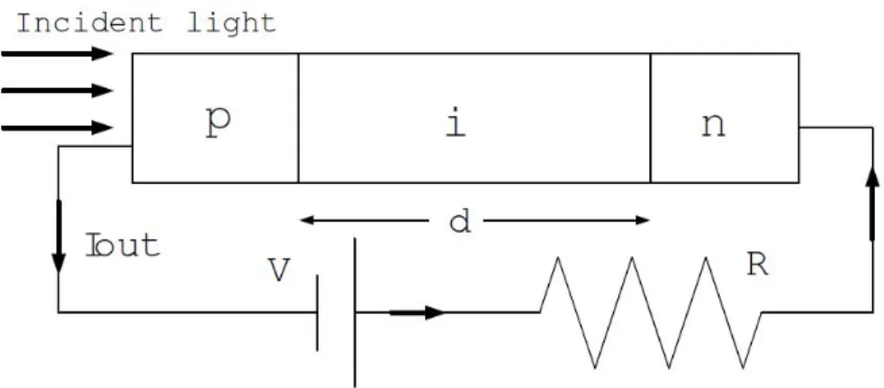
P-I-N Photodiodes
A p-i-n photodiode is simply a p-n junction with an intrinsic layer sandwiched between p and n type doped layers. It operates in reverse bias mode and it is suitable for high quantum effıciency operation due to its intrinsic layer. However, generally homojunction p-i-n photodiodes lack in high-speed operation because there is a diffusion component in the output current. The photo-generated carriers outside the depletion region diffuse into the intrinsic i region and in the depletion region they are swept away by the electric field. Since diffusing is slower than drifting in high electric field, p-i-n photodiodes are much slower than Schottky
Figure 2.1.4 Schematics of a p-i-n photodiode
photodiodes. This problem can be solved by using p and n layers which have higher band gaps than intrinsic layer so that photo-generation occurs only in the intrinsic region. In this way, high efficiency and high speed p-i-n photodiodes can be designed.
Avalanche photodiodes
An avalanche photodiode (APD) operates by converting each detected photon
into a cascade of moving carrier pairs. With APDs, we have large photocurrent in the external circuit compared to the photo-generated photocurrent resulting from
11
a very weak optical signal. By impact ionization process under high electric field, we have internal gain in the depletion region. For the avalanche multiplication to occur devices are operated at high voltages in the breakdown region usually avoided in normal operation.
The high electric field in the depletion region accelerates the photo-generated charges, causing them to have kinetic energy large enough to ionize the crystal lattice with the resulting new electron-hole pairs. The new charge carriers are also accelerated and avalanche multiplied as well.
Figure 2.1.5 Reach-through p+-π-p-n+ APD structure. The π region is very lightly doped p- type material.The p + and n + regions are heavily doped [23].
Since during the avalanche process, we have high electric field in the depletion region, APDs are fast devices compared to other devices with internal gain. In a material with avalanche gain, the impact ionization can be described by the ionization coefficients alpha and beta of electron and hole which is defined as the number of new pairs generated for unit length by the carrier under a certain electric field. The inverse of alpha and beta are the ionization lengths and represent the mean free path between successive multiplications. The ionization coefficients increase with the electric field in the depletion region and decreases with the device temperature.
12
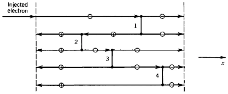
Ionization ratio can be defined as the ratio of the ionization coefficients and symbolized with the letter k. When k is very small this means that holes do not ionize substantially with regard to electrons so most of the ionization is realized by electrons. The multiplication terminates when all of the electrons reach the n side of the depletion layer. However, if the k is close to 1, there will be a positive feedback and we have an enormous gain. This is, on the other hand, is not desirable for the following reasons. It takes more time for the hole to process this in turn decreases the bandwidth. Device noise increases because the process is
Figure 2.1.6Constancy of the sum of the electron and hole current densities across a plane at any x. By way of illustration, four impact ionizations and five electrons-plus-holes crossing every plane are illustrated [23].
intrinsically random. Since we have very high gain, the device is unstable and this causes the device to get into avalanche breakdown.
It is advantages to use materials in the APD structures having k values either close to 0 or very large. For instance, if material favors the electrons with regards to impact ionization, optimal gain is achieved when the electrons are injected at the p-type layer of the depletion layer.
We will first consider the simpler problem of single-carrier (electron) multiplication (h ,0 k ). Let ( )0 J x be the electric current density carried e by electrons at location x, as shown in the figure. Within a distance dx, on the average, the current is incremented by the factor,
13
( ) ( )
e e e
dJ x J x dx,
From which we obtain the differential equation, ( ) e e e dJ J x dx ,
Whose solution is the exponential function ( )J xe Je(0) exp(ex). The gain ( ) / (0)
e e
G J W J is therefore
exp( e )
G W .
The electric current density increases exponentially with the product of the ionization coefficient e and the multiplication layer width W.
The double-carrier multiplication problem requires knowledge of both the electron current density ( )J x and the hole current densitye J x . It is assumed h( ) that only electrons are injected into the multiplication region. Since hole ionizations also produce electrons, however, the growth of ( )J x is governed by e
the differential equation.
( ) ( ) e e e h dJ J x hJ x dx ,
As a result of charge neutrality,dJ dxe/ dJh/dx, so that the sum
( ) ( )
e h
J x J x must remain constant for all x under steady-state conditions. This is clear from fig.; the total number of charge carriers crossing any plane is the same regardless of position,
Since it is assumed that no holes are injected at x W ,J Wh( ) 0 , so that
( ) ( ) ( )
e h e
J x J x J W ,
The hole current density J x can therefore be eliminated in the equation to h( ) obtain ( ) ( ) ( ) e e h e h e dJ J x J W dx .
14
The first-order differential equation is readily be solved for the gain ( ) / (0)
e e
G J W J .
For e hthe result isG( e h) /
eexp (
e h)W
h
, from which we obtain
1
exp (1 ) e k G k W k .The single-carrier multiplication result for gain, with its exponential growth, is recovered when k=0. When k is infinity, the gain remains unity because only the electrons are injected and electrons do not multiply. For k=1, the equation becomes indeterminate and gain must be obtained directly from. The result is thenG1/ (1eW). Instability is reached wheneW . The dependence of the 1 gain on eW for several values of the ionization ratio k is illustrated in figure 2.1.7.
Figure 2.1.7 Growth of the gain G with multiplication-layer width for several values of the ionization ratio k, assuming pure electron injection [23].
15
Diode Characteristics
Photodiodes characterization composed of I-V (current-voltage) measurement, quantum efficiency, high speed (bandwidth) measurement. Performance of a photodiode is tested via these characterizations.
Current-Voltage Characteristics
Low dark current and high breakdown voltage are two parameters to test the photodiode quality. Dark current is the current flowing in the reverse bias with no illumination. A device with lower dark current is likely to be more sensitive. We cannot apply a reverse bias voltage as high as we like through a photodetector because after a certain voltage photodiode enters into avalanche breakdown which puts a limit on the reverse bias voltage that can be applied for photodiode operation.
Quantum Efficiency
The quantum efficiency η (0≤η≤1) of a photodetector is defined as the probability that a single photon incident on the device generates a photo-carrier pair that contributes to the detector current. When many photons are incident, as is almost always the case, η is the ratio of the flux of generated electron-hole pairs that contribute to the detector current to the flux of incident photons. Not all incident photons produce electron-hole pairs because not all incident photons are absorbed. Some photons may be reflected from the surface of the photodetector, or photo-generated pairs near the surface recombine due to the abundant recombination centers and fail to contribute to the current. The quantum efficiency can therefore be written as,
(1 R) 1 exp(
d)
16
d is the thickness of the absorbing semiconductor layer, and ς is the fraction of electron-hole pairs that contribute to the detector current.
Bandwidth
As mentioned previously, the response time of a photodetector is mainly limited by the transit times of the photo-generated carriers. RC time constant of the photodiode circuit and diffusion of carriers in the undepleted regions also impose limitations on the response time of a photodetector.
Schottky and heterojunction photodetector designs can be used to resolve the carrier diffusion problem either by decreasing the undepleted regions as in Schottky diodes or using different band gap materials as in heterojunction photodiodes.
The impulse-response function is determined by convolving i(t) with the exponential function (1/RC) exp( /t RC).When we decrease d (depletion width), the capacitance of the junction increases. Transit time also decreases when we decrease d. The transit times and capacitance limited 3-dB bandwidths can be written as:
ftr 0.45 d 2 RC d f R A
By decreasing d we can increase bandwidth as long as we use small devices so that the capacitance of the devices decreases accordingly. So if we consider only transit time limitation, bandwidth of the photodetector is inversely proportional to d.
17
Bandwidth-Efficiency Trade-off
The bandwidth-efficiency product determines the overall performance of a photodiode. Bandwidth and efficiency have inverse dependencies on active layer thickness, d. High quantum efficiencies near unity and bandwidth can be achieved with very thick and very thin active layers respectively but their product for a given d is almost constant. To increase bandwidth-efficiency product, we have to makeuse of resonant cavity enhancement effect (RCE).
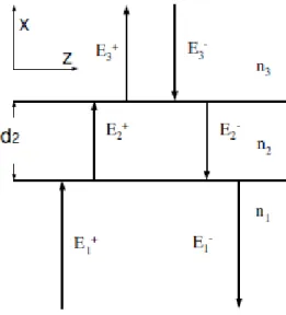
Figure 2.2.1Reflection and transmission of an electromagnetic wave incident on a dielectric film of thickness d2.
2.2 Optical Design using TMM code
In this chapter, we will explain the optical simulation of our photodetector designs using TMM (Transfer matrix multiplication) code.
Assuming the incident light is in the form of polarized plane waves and it is vertical to the plane of interface between the two media, we can write the electric field vector as,
( )
0
t ik r
E E e
18
Therefore we can write the electric fields in three regions as the following.
1 1 2 2 3 2 3 3 2 3 -ik x ik x + -1 1 -ik x ik x + -2 2 2 ik -ik x ik ik x + -3 3
ˆ
ˆ
yE e +yE e ; x<0
ˆ
ˆ
yE e
+yE e ; 0<x<d
ˆ
ˆ
yE e e +yE e e
d dE
2; x>d
0 ( ) ; 1, 2,3 i i i k n k n i c 1, , 2 and 3n n n are refractive indices and 0 0 2 k c
denotes the free space wave number. The implicit ei t dependence
has been suppressed and therefore the superscripts + and – correspond to waves propagating in the +x and –x directions respectively.
The corresponding magnetic fields can be calculated by using the formula, H kx E And are given by
1 1 2 2 -ik x ik x + -1 1 1 1 0 0 -ik x ik x + -2 2 2 2 2 0 0 i + 3 3 0 z E e -z E e ; x<0 z E e -z E e ; 0<x<d z E e n n c c n n H c c n c k3 2 -ik x3 3 - ik3 2 ik x3 3 2 0 e -z E e e ; x>d d n d c
Where the media are assumed to be nonmagnetic with 0. Since both E and H represent tangential components, they must be continuous at x=0 and at x=d2.
Continuity at x=0 gives,
E1E1 E2E2, n E1( 1 E1) n E2( 2 E2)
19 1 2 1 2 1 1 1 1 2 2 1 1 1 r E E E S r t E E E ,
Where r1 and t1 are the amplitude reflection and transmission coefficients at
the first interface and given by 1 2 1 1 2 n n r n n 1 1 1 2 2n t n n Continuity of the fields at x=d2 gives,
2 2 2 2 3 3 2 2 2 2 3 3 2 2 1 i i i i E E E e r e S t E E E r e e
Where r2 and t2 are the amplitude reflection and transmission coefficients at the
second interface
2 k d2 2k n d0 2 2then we can combine equations
1 3 3 3 3 1 a b E E E S c d E E E
Now in the third medium there will not be any reflected wave and as such
3 0
E . This immediately gives us,
1 3
E aE
1 3
E cE
And therefore the amplitude reflection and transmission coefficients of the film are given by 1 1 E c r E a 3 1 1 E t E a
20 2 2 2 1 2 1 2 2 2 2 1 2 1 2 2 2 cos 2 1 2 cos 2 r r r r R r r r r r 2 2 2 3 3 1 2 2 2 1 11 1 2 21 2cos 2 2 n n t t T t n n r r r r
Upon substituting the related values for r and t, we obtain
1
R T
Furthermore whencos 22 , i.e., when 1 2 ( 1) ; m=0,1,2,... 2 m or 0 0 0 2 2 2 2 3 5 d , , ,... 4n 4n 4n
minimum reflectivity is achieved (for r1r2>0) and it is
given by, 2 2 2 1 3 2 1 2 2 1 2 1 3 2 1 n n n r r R r r n n n
Thus the reflectivity will be zero when
1 2
2 ( 1 3)
n n n . The reflectivity of the surface can be made zero at any chosen wavelength c by choosing the film thickness to be 2 4 c n
. This technique of reducing the reflectivity of a surface is known as blooming and the surface is said to be anti-reflected coated.
When cos 22 , i.e., when 1 0 0 0 2 2 2 2 2 3 , , ,... 2 2 2 d n n n
the reflectivity is given by
2 3 1 3 1 n n R n n
which is independent of the refractive index of the intermediate film.
For the case of two films, with r3 and t3 are the amplitudes of reflection and
transmission coefficients between media 3 and 4 and 3k d3 3k n d0 3 3 Thus
21 1 4 1 4 E E S E E where S S S S 1 2 3
Similarly one can obtain expressions for the reflectivity and transmittivity. Generalizing the above analysis for N films and for oblique incidence, we may write 1 2 2 1 N N E E S E E where SS S S1 2 3...SN1 and 1 j j j j i i j j i i j j e r e S t r e e and 1 0 0 2 cos cos ; 2,3, 4,..., ( 1) j k dj j j n dj j j j N
and rj and tj are the amplitude reflection and transmission coefficients between media with refractive indices nj and nj+1.
Using snell’s law, jcan also be expressed as, 1 2 2 2 2 1 1 0 2 ( sin ) j d nj j n .
This method can be used to calculate the transmission, reflection and absorption at any layer and is called the transfer matrix method (TMM).
Distributed Bragg Mirrors (DBR's) are widely used in optoelectronic applications such as detectors and semiconductor lasers. A DBR is a stack consisting of periodically alternating quarter-wave thick material layer pairs whose refractive indices are different at the wavelength region of interest. Each pair consists of two layers having thicknesses of c/ 4n1 and c/ 4n2 respectively and c is the central wavelength of the mirror where reflectivity is maximum. All the light reflected from different interfaces of the DBR has the
22
same phase resulting in constructive interference therefore we have very high reflectivity. Using TMM method for a DBR consisting of N pairs, the reflectivity at the center wavelength can be expressed as,
2 2 2 1 2 max 2 2 1 2 N N N N n n R n n
This formula is valid when the stack is in the air, but for the first and the last layers which are different than air, we have to modify the formula as,
2 2 0 max 2 0 ( ) 1 ( ) 1 N L s H N L s H n n n n R n n n n
where n and 0 n are refractive s
indices of air and substrate medium. We assumed that the thickness of the substrate layer is infinite, since it is significantly thicker than the other layers in the wafer structure.
We can illustrate this situation by growing DBR pairs consisting of SiO2 and
Si3N4 since at 350nm Si3N4 is grown on SiO2 to have an enhancement in
reflectivity. The appropriate thickness for DBR layers can be calculated using the formulac / 4n, where n is the layer’s refractive index atc. For
350
c nm
, this results in the thicknesses of 49.7 nm and 59.5 nm for Si3N4
and SiO2 respectively. By increasing the number of DBR pairs, we can obtain
23
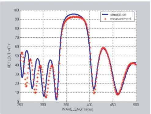
Figure 2.2.2 Reflectivity of 8 pairs of DBR on GaAs substrate.
The figure 2.2.2 shows the reflectivity of 8 pairs of DBR on GaAs substrate and it is close to unity.
24
Chapter 3
Fabrication and Characterization
In this chapter, fabrication processes and the characterization methods will be presented. Fabrications and characterizations were carried out in both Nanotechnology Research Center Lab and Advanced Research Lab at Bilkent University which has a class 100 clean room having a dust count of 100 particles per cubic foot volume. This corresponds to 3500 particles (with particles diameters of 0.5 micron or larger) per cubic meter.
Sample preparation
First, we have to obtain a sample large enough to handle with tweezer but not too large since the epitaxial wafers are very expensive. The mask size is 7x7 mm2. The cleanness of the sample, the chemicals used, and the environment are very important for a successful fabrication. To cleave the wafer, we use a diamond tipped scriber-pen. After defining the line of the cut on the backside of the wafer which is not polished, we press the scribers tip at the edge of the wafer. Unfortunately it is not easy to obtain GaN, or AlGaN wafers in the desired size or shape. When the scriber’s tip is pressed on the wafer, it may crack into various small pieces. Therefore, the samples are difficult to handle and process.
At the beginning of every step, we have to do a three-solvent-cleaning (TSC) process. Trichloroethane dissolves oil, acetone dissolves photoresist, organic molecules, and trichloroethane, and isopropanol dissolves acetone and water dissolves the acetone. Samples are placed into a teflon basket and immersed into a boiling trichloroethane for two minutes, then into acetone at room temperature for five minutes, then into boiling isopropanol for 2 minutes. Samples are exposed to the deionized water (DI) flow and then dried with a nitrogen gun.
25
Samples are baked on a hot plate at 120 °C for 2 minutes which called dehydration bake. Finally, the samples surfaces are examined under an optical microscope.
Normal photolithography
AZ 5214E type photoresist has an absorption peak at around 360 nm and we perform the UV exposure with an Hg lamp which has a line at 365 nm. Mask alignment is done with a Karl-Suss MJB3 mask aligner. Mask alignment is accomplished by means of alignment marks. After pre-bake, the sample is is aligned with the mask. Then the sample is exposed to the UV radiation for 20 seconds with an optical power of 8mW/cm2 for a total dose of 160 mJ/cm2.
Image Reversal Photolithography
In this technique the transparent parts of the mask will be transferred onto the resist, so that the mask is different from the mask used in normal lithography. The resist covered sample is aligned with the image-reversed mask and exposed with an optical power of 8mW/cm2 for 8 seconds. Then the sample is baked for 2 minutes at 110 °C on a hot plate. The sample is exposed for 18 seconds without mask which is called flood exposure. These two additional processes change the photoresist so that the frst exposed regions behave as non-exposed regions and vice versa. Therefore the additional bake is very critical in image reversal lithography. The optimization is done by changing the image reversal bake time and the bake temperature. Image reversal photolithography makes the lift-off of thick metallization easy. Normally, the exposure is larger near the top of any resist, which results in a more rapid development near the surface and leads to a resist profile with a positive slope for positive resists. However, after image reversal this profile is also reversed, resulting in an undercut profile.
26
Development
AZ 400K developer is used with a 1:4 ratio of developer to DI water for the development of the exposed samples. In the normal photolithography the exposed regions of resist are etched while in the image reversal photolithography the non- exposed regions are etched. The development time is determined by using a dummy GaAs sample since we cannot observe the color change on a GaN or AlxGa1-xN sample since it is transparent. In development, we use a white basket
to observe the color change easily. When the color change has stopped, the samples are rinsed under DI water flow. By this method, we find the development time to be approximately 43-47 seconds with a thickness of 1.4micron. Then the sample is dried with a nitrogen gun. The samples are put under an optical microscope, the resolution patterns should be sharp and 1micron resolution should be observed for a good photolithography. Mask alignment is observed via the alignment marks.
Etching Techniques:
In processing of the wafer, we have to etch through the wafer surface. For example, we have to make contacts to an epitaxial layer buried under the surface of the wafer, second we must isolate devices by making mesas , third must make contacts to metalizations beneath the silicon nitride. Etching can be divided into wet (aqueous solution) etching and dry etching (Reactive Ion Etching).
Chemical etching techniques in liquid or gaseous environment is used to remove any barrier material not protected by hardened photoresist. The chemicals we choose depends on the material which we desire to etch. A high degree of selectivity is required so that the etchant will remove the unprotected areas much more rapidly than the photoresist layer. People use metals or other dielectric material as protection mask other than the photoresist.
27
Wet Chemical Etching
For silicon wafers, buffered oxide etch is commonly used to etch windows in silicon dioxide layers. BOE is a solution containing HF (hydrofluoric acid), and etching is performed by immersing the wafers in the solution. HF at room temperature etches silicon dioxide much more rapidly than it etches photoresist or silicon. The etch rates depend on the oxide density, acid density, and temperature so these parameters should be controlled for the desired etch depth.
Wet chemical etching is an isotropic process, etching equally in all directions. This “etch bias” is a serious problem in processes requiring linewidths with dimensions similar to the thickness of the film.
Chemical solvents are used to wet etch semiconductor and dielectric materials. GaAs etchant is frst to oxidize the surface with an oxidizing agent and second to remove the oxidized layer with acid or base. In our processes we use H2O2/NH3/H2O (2.4:8:300) as etchant with an etch rate of 50 Angstrom/sec. at room temperature. Dielectric materials SiO2, Si3N4 can be etched with HF. ITO can also be etched via HF. HF in aqueous form is very dangerous so we have to be very careful in using it. We use a dilute HF / DI water (1:30) in nitride etching at a rate of 400 Angstrom/sec.
Dry Etching
Dry etching is highly anisotropic process therefore, very anisotropic profiles can be obtained, without having the problem of undercutting problem which is a characteristic of wet etch processes. Dry etch processes need only small amount of reactant gases, on the other hand, wet etching results in disposal of a relatively large amounts of liquid chemical wastes.
Plasma etching immerses the wafers in a gaseous plasma created by RF excitation in a vacuum system. The plasma contains fluorine or chlorine ions which etch silicon dioxide. Sputter etching uses energetic noble gas ions such as Ar+ to bombard the wafer surface. Etching process occurs by physically knocking atoms off the surface of the wafer. Highly anisotropic etching can be
28
obtained, but selectivity is not good. Metals can be used as barrier materials to protect the wafer from etching.
Reactive ion etching combines the plasma and sputter etching processes. Plasma systems are used to ionize reactive gases, and the ions are accelerated to bombard the surface. Etching process occurs through a combination of the chemical reaction and momentum transfer from the etching species.
In our system, we use ultra high vacuum RIE machine for dry etching. Photoresist and dielectric materials are etched with plasma ions hitting the sample surface. Using different gases in the plasma we can etch different materials. O2 is used to etch photoresist film. CCl2F2 etches SiO2, Si3N4, and ITO. Si3N4 can also be etched with CHF3. In our fabrication GaN and AlxGa1-xN are etched with
CCl2F2.
Photoreist removal
After windows are etched through the SiO2 layer, the photoresist is stripped from the surface, leaving a window in the silicon dioxide. Photoresist removal typically uses proprietary-liquid resist strippers, which cause the resist to swell and lose adhesion to the substrate surface. Dry etching may also be used to remove resist by oxidizing (burning process) it in oxygen plasma, a process which is often called resist ashing.
29
Metalization
In our processes we use the lift-off metallization technique to make ohmic and schottky contacts, and interconnects between them. Once the required metallization layout is defined by photolithography, the samples are coated by desired metals. Since the photoresist film has a finite thickness, the coated material (if it is thin enough) is discontinuous at the pattern edges of the resist. Therefore, in acetone the photoresist dissolves lifting off the material on it. The metals are deposited onto the samples via UHV LE590 box coater. Metals in powder or solid form are placed in tungsten boats. UHV causes the metal to evaporate in lower temperature.
Samples are placed over the boats. Short holder is used to decrease the usage of metals but we have to be careful watching the sensors display since the holder is half of the long holder the actual deposition rate is four times the displayed value. When the desired pressure is reached, current is passed through the tungsten boats and metal deposition takes place.
Annealing
To make metal semiconductor contacts ohmic we use rapid thermal process (RTP) in which samples are heated up to very high temperatures in very short time. Within 20-30 seconds, the metal contact melts and diffuses into the semiconductor and the barrier electrons encounter becomes very low as a result the contact resistance becomes ohmic. Flash lamps are used as the heating source. From the figure one can notice the cheese like structure on the ohmic contact which is an indicator of a good ohmic contact.
Plasma Enhanced Chemical Vapor Deposition
(PECVD)
Dielectric films are used mainly to protect the devices on the wafer. Silicon nitride films can be used for passivating devices, because they serve as barriers
30
to the diffusion of water and sodium. Silicon nitride oxidizes very slowly and prevents the underlying layers from oxidation. In our processes, PECVD is used to deposit silicon nitride and silicon oxide at relatively low temperatures with respect to other methods otherwise high temperature can affect the ohmic contacts. Dielectric coatings can also be used as anti-reflection or reflection coatings. To deposit Si3N4, we used silane (2%SiH4+98%N2) and ammonia (NH3) gases at 250 °C at a deposition rate of 140 A/min.
Lift-off
After metalization, the sample is left in acetone. Acetone dissolves the photoresist and the metal deposited on it will be lifted off and only the metal on the open area of the resist will remain on the sample surface. In order to get a good lift-off, we should wait a few hours and if the lift- off is not complete we should spray the sample with acetone. In the case of thick metallization ( > 1micron) we may need ultrasound application, however this is a bit risky it may remove the metal which should stay on the sample surface. Therefore ultrasound must be applied in short time duration for instance a few seconds.
31
Chapter 4
Research on GaN/Al
x
Ga
1-x
N
In this chapter, the work on the GaN/AlGaN based Schottky, p-i-n, and avalanche type photodetectors will be presented. Details of their designs, fabrication and the measurement results will be demonstrated.
4.1 Schottky Contact Photodetector
AlGaN Schottky photodiodes do not suffer from p+ contact problems. High quality Schottky and n+ ohmic contacts on AlGaN layers can be formed using standard processes. In addition, the temporal pulse response of Schottky detectors is not degraded by minority carrier diffusion which makes them suitable for high-speed operation [24,25,26]. Using these properties, high performance solar-blind AlGaN Schottky photodiodes were reported by several research groups [27,28,29]. Recently, we have demonstrated solar-blind AlGaN Schottky photodiodes with low dark current and high detectivity performance
[30]. The bandwidth of these detectors was below the GHz level [31]. In this study, we report low dark current solar-blind AlGaN Schottky photodiodes with improved leakage and bandwidth performance. Leakage current of a few fA and bandwidth-efficiency product of 2.9GHz was achieved with the fabricated solar-blind AlGaN Schottky detectors.
Fabrication
The solar-blind devices were fabricated on MOCVD grown Al0.38Ga0.62N/GaN
32
micron thick Al0.38Ga0.62N absorption layer. For ohmic contacts, highly doped
n+ GaN layer was utilized. Fabrication process of the AlGaN Schottky photodiodes was accomplished using a microwave compatible five mask-level standard semiconductor process. In sequence, ohmic contact formation, mesa isolation, Schottky contact formation, surface passivation, and interconnect metallization steps were completed. Etching process of AlGaN/GaN layers was done using a reactive ion etching (RIE) system. Ti/Al alloy was used as ohmic contact metal. Schottky contacts were formed with thin (100Angstrom) semitransparent Au films.
Measurements
The fabricated devices were characterized in terms of current–voltage (I–V), spectral responsivity, and temporal pulse response. All measurements were made on wafer at room temperature using a low-noise microwave probe station. I–V measurements were performed with a high-resistance Keithley 6517A electrometer which featured a sub-fA current measurement resolution (Figure 4.1.1). However, mainly due to the pick-up noise from the environment and cables, the dark current measurements were limited by the 2 fA background current floor of the setup. Spectral responsivity measurements were done using a 175W xenon light-source, a monochromator, multi-mode UV fiber, lock-in amplifier and a calibrated Si-based optical power-meter. The UV-illuminated solar-blind detectors were biased with a DC voltage source, and the resulting photocurrent was measured using the lock-in amplifier. Temporal high frequency measurements were done at 267nm. Ultrafast UV pulses were generated using a laser set-up with two nonlinear crystals. A Coherent Mira 900F model femtosecond mode-locked Ti:sapphire laser was used to generate the pump beam at 800nm. The pump pulses were produced with 76MHz repetition rate and 140 fs pulse duration. These pulses were frequency doubled to generate a second harmonic beam at 400nm using a 0.5mm thick type-I b-BaB2O4 (BBO) crystal. The second harmonic beam and the remaining part of
33
the pump beam were frequency summed to generate a third harmonic output beam at 267nm
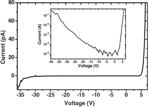
Figure 4.1.1 Dark current of a 30lm diameter solar-blind AlGaN photodiode.The inset shows the same plot in logarithmic scale.
using another type-IBBO crystal with thickness of 0.3mm. The resulting 267nm pulses had <1ps pulse-width and were focused onto the devices using UV enhanced mirrors and lenses. The detectors were biased using a DC voltage source and a 26GHz bias-tee. The resulting temporal pulse response was observed with a 20GHz sampling oscilloscope.
34
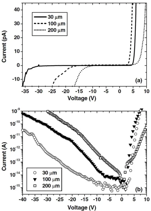
Figure 4.1.2 –V curves of AlGaN Schottky detectors with different device areas: (a) linear scale, (b) logarithmic scale.
35
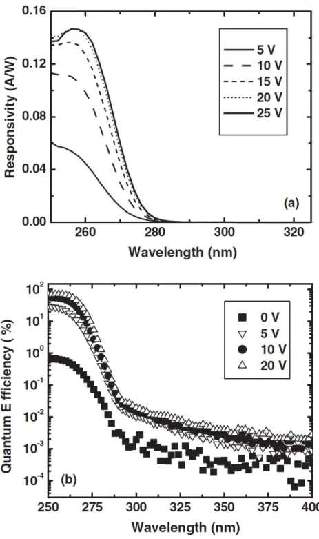
Figure 4.1.3 (a) Measured spectral responsivity curves as a function of reverse bias voltage, (b) corresponding spectral quantum efficiency of Schottky photodiodes.
36
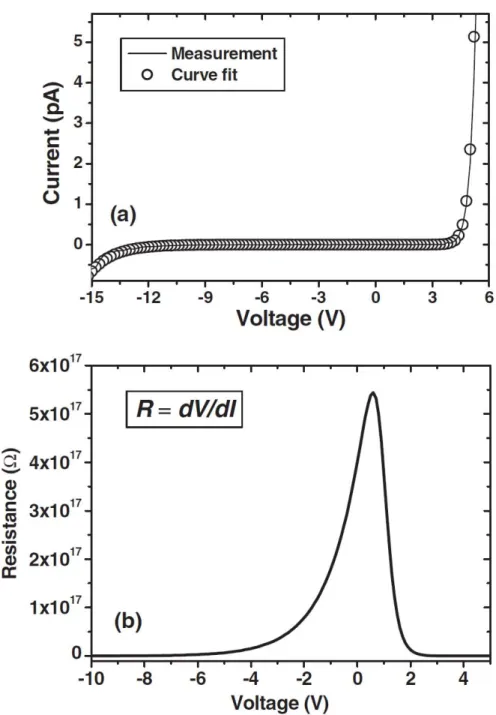
Extremely low leakage currents were observed in the fabricated AlGaN Schottky photodiode samples. Fig. 4.1.1 shows the measured I–V curve of a small area (30lm diameter) device. The solar-blind device exhibited leakage current less than 3fA and 10fA for reverse bias up to 12V and 17V respectively. Under <12V reverse bias, the measured dark current fluctuated below the 3fA level due to the background noise of the setup. Sub-fA leakage currents were observed in this range. Using an exponential fit, we estimate the zero bias dark current less than 0.1 fA. The corresponding dark current density for this device at 12V was 4.2x10⁻¹⁰A/cm2. Typical reverse breakdown voltages were measured
to be higher than 50V. In the forward bias regime, turn-on characteristic was observed at ~4V. Current in this regime increases with a much slower rate than in an ideal photodiode. At 10V bias, forward current was only 35nA. We attribute this result to the high series resistance of the devices. I–V measurements of larger area devices resulted in higher leakage currents. Fig.
4.1.2(a) and (b) show the dark I–V curves of 30µm, 100µm, and 200µm
diameter devices in linear and logarithmic scale respectively. 200µm device displayed the largest dark current. We measured the reverse bias values where the devices displayed 1pA leakage current. For 30, 100, and 200 micro meter diameter detectors, 1pA dark current was reached at -32V, -18V, and -12V respectively. To make a fair leakage comparison between the devices, the current density values at 5V reverse bias were calculated.
37
Figure 4.1.4 (a) Linear plot of I–V data and exponential fit for a 30lm diameter AlGaN detector, (b) calculated differential resistance for the same device.
100 µm and 200 µm devices exhibited 7fA and 67fA dark current at -5V, which leaded to 8.9 ·x10-11A/cm2 and 2.1x10⁻¹⁰A/cm2 dark current density values respectively. Due to the experimental setup limit, the actual dark current density
38
of 30 µm device at 5V reverse bias could only be estimated by exponential fitting curve as 3.3 x 10⁻¹¹A/cm2. These results correspond to the lowest leakage performance reported for AlGaN-based Schottky photodiodes. As expected, lower breakdown voltages were observed with increasing detector size. Turn-on voltages of -2.5V and -5V were measured for 100 µm and 200 µm devices respectively.
Spectral photoresponse of solar-blind AlGaN detectors was measured in the 250–400nm spectral range. The bias dependent measured spectral responsivity and quantum efficiency curves are plotted in Fig. 4.1.3.(a) shows the strong bias dependence of device responsivity. The peak reponsivity increased from 61mA/W at 250nm to 147mA/W at 256nm when applied reverse bias was increased from 5V to 20V. The device responsivity saturated for >20V reverse bias, which indicates the total depletion of undoped Al0.38Ga0.62N absorption
layer. A sharp decrease in responsivity was observed at ~265nm. The cut-off wavelength of the detectors was found as ~267nm, which ensured the true solar-blind operation of our detectors. Fig. 4.1.3(b) shows the semilog plot of the corresponding spectral quantum efficiency The photovoltaic (zero bias) quantum efficiency was very low. When the bias was increased to 5V, the efficiency was drastically improved by a factor more than 20. The low zero-bias efficiency value and strong bias dependent characteristic of device responsivity indicates photoconductive gain-assisted device operation. The observed photoconductive gain can be explained by the carrier trapping mechanism in Al0.38Ga0.62N active layer. Pulse response measurements have confirmed our suggestion with carrier trapping limited high-speed results. A maximum efficiency of 71% at 256nm was measured under 20V reverse bias. The visible rejection reached a maximum of ~4 x10⁴ at 10V reverse bias. The detectivity performance of solar-blind detectors is thermally limited since the background radiation within the solar-blind spectrum is very low compared to thermal noise. Therefore, detectivity of solar-blind detectors can be expressed by *
4 o R A D R kT where Rλ
![Figure 2.1.5 Reach-through p+-π-p-n+ APD structure. The π region is very lightly doped p- type material.The p + and n + regions are heavily doped [23]](https://thumb-eu.123doks.com/thumbv2/9libnet/5762399.116607/27.918.250.594.419.710/figure-reach-structure-region-lightly-material-regions-heavily.webp)
![Figure 2.1.7 Growth of the gain G with multiplication-layer width for several values of the ionization ratio k, assuming pure electron injection [23]](https://thumb-eu.123doks.com/thumbv2/9libnet/5762399.116607/30.918.221.557.671.927/figure-growth-multiplication-values-ionization-assuming-electron-injection.webp)