a dissertation submitted to
the department of physics
and the institute of engineering and science
of bilkent university
in partial fulfillment of the requirements
for the degree of
doctor of philosophy
By
Sefa Da˘g
June, 2005
I certify that I have read this thesis and that in my opinion it is fully adequate, in scope and in quality, as a dissertation for the degree of doctor of philosophy.
Prof. Dr. Salim C¸ ıracı(Supervisor)
I certify that I have read this thesis and that in my opinion it is fully adequate, in scope and in quality, as a dissertation for the degree of doctor of philosophy.
Prof. Dr. Atilla Er¸celebi
I certify that I have read this thesis and that in my opinion it is fully adequate, in scope and in quality, as a dissertation for the degree of doctor of philosophy.
Prof. Dr. Atilla Aydınlı
Prof. Dr. S¸efik S¨uzer
I certify that I have read this thesis and that in my opinion it is fully adequate, in scope and in quality, as a dissertation for the degree of doctor of philosophy.
Prof. Dr. S¸akir Erko¸c
Approved for the Institute of Engineering and Science:
Prof. Dr. Mehmet B. Baray Director of the Institute
ABSTRACT
FUNCTIONALIZATION OF CARBON NANOTUBES
Sefa Da˘g PhD in Physics
Supervisors: Prof. Dr. Salim C¸ ıracı June, 2005
Carbon nanotubes, in which two-dimensional hexagonal lattice of graphene is transformed to a quasi one-dimensional lattice that conserves the local bond arrangement, provide several structural parameters to engineer novel structures with desired properties allowing ultimate miniaturization. Most of the effort has gone to reveal various physical properties of nanotubes and to functionalize them by external agents. This thesis covers the investigation of electrical, mechanical, magnetic and contact properties of single wall carbon nanotubes functionalized with deformation, doping, coating, etc. All investigations in this thesis are based on the first principles calculations.
At the beginning, the adsorption of individual atoms and molecules on the semiconducting and metallic single-walled carbon nanotubes (SWNT) has been investigated. First calculations cover an extensive and systematic analysis of the oxygenation of semiconducting and metallic single-wall carbon nanotubes. The physisorption of oxygen molecules, chemisorption of oxygen atoms and forma-tion of an oxide, as well as the equilibrium binding geometry and corresponding electronic energy structure have been treated. Apart from oxygen, the stable ad-sorption geometries and binding energies have been determined for a large number of foreign atoms ranging from alkali and simple metals to the transition metals and group IV elements. We found that the character of the bonding and associ-ated physical properties such as electronic, magnetic and mechanical properties strongly depend on the type of adsorbed atoms, in particular, on their valence electron structure.
Nanotube coverage is one of the important phenomena to produce metallic nanowires and high-conducting interconnects in nanoelectronics. We were in-terested in preparing decorated nanotubes by using transition-metal atoms onto nanotube surfaces. We have shown that a semiconducting SWNT can only be
covered uniformly by titanium atoms and form a complex but regular atomic structure. The circular cross section of the tube changes to a square-like form, and the system becomes metallic with high state density at the Fermi level, and with high quantum ballistic conductance. Even more interesting is that uniform titanium covered tubes have magnetic ground state with significant net magnetic moment. Other than Ti, Ga is also shown to be a potential element that can make good conducting wires through coverage of SWNTs.
We report the crossed junctions which are modelled by two-dimensional grids of zigzag SWNTs. The atomic and electronic structure, stability, and energetics of the junctions are studied for different magnitudes of contact forces pressing the tubes towards each other and hence inducing radial deformations. The intertube conductance through such a junction diminish because of finite potential barrier intervening between the tubes. On the other hand, our study of the contact between a semiconducting SWNT and metal electrodes shows that the electronic structure and potential depend strongly on the type of metal.
Because of high surface-volume ratio nanotubes are also considered impor-tant systems for hydrogen storage. We demonstrated that hydrogen molecule can not bind to SWNT surface. But the character of the bonding changes dra-matically when SWNT is functionalized by the adsorption of Pt atom. Single H2
is chemisorbed to Pt atom on the SWNT either dissociatively or molecularly. If Pt-SWNT bond is weakened either by displacing Pt from bridge site to a specific position or by increasing number of the adsorbed H2, the dissociative adsorption
of H2 is favored. Present results reveal the important effect of transition metal
atom adsorbed on SWNT and advance our understanding of the molecular and dissociative adsorption of hydrogen for efficient hydrogen storage. In particular, they led to the study of Ti adsorbed SWNT on the adsorption of hydrogen. It is reported that a single Ti atom coated on a SWNT binds up to four hydrogen molecules. The first H2 adsorption is dissociative with no energy barrier while
the other three adsorptions are molecular with significantly elongated H-H bonds. We carried the adsorption of H2 on the innerwall of SWNT to increase the
stor-age capacity further. These results advance our fundamental understanding of dissociative adsorption of hydrogen in nanostructures and suggest new routes to better storage and catalyst materials.
vi
Keywords: Carbon Nanotube, Ab-initio, Density Functional Theory, Function-alization, Transition Metal, Hydrogen Storage, Contact.
KARBON NANOT ¨
UPLER˙IN
FONKS˙IYONELLES
¸T˙IR˙ILMES˙I
Sefa Da˘g Fizik, Doktora
Tez Y¨oneticisi: Prof. Dr. Salim C¸ ıracı Haziran, 2005
Karbon nanot¨upler, grafitin iki boyutlu hekzagonal ¨org¨un¨un silindirik, bir boyutumsu ¨org¨uye d¨on¨u¸sm¨u¸s halidir. Bu d¨on¨u¸s¨um esnasında yerel ba˘g d¨uzeni ko-runur. Bu yapılar, en a¸sırı minyat¨urle¸stirme ile arzu edilen ¨ozelliklerde alı¸sılmadık yapıların tasarlanabilmesini sa˘glayacak ¸cok farklı yapısal niteliklere sahiptir. G¨un¨um¨uzde bu konuda yapılan ¸calı¸smalar, nanot¨uplerin fiziksel ¨ozelliklerini or-taya ¸cıkarma ve dı¸s etkenler yardımıyla nasıl fonksiyonel hale getirilebilece˘gini an-lamaya y¨oneliktir. Bu tez ¸calı¸sması, esas olarak, karbon nanot¨uplerin katkılama ve kaplama etkisi ile yapısal, elektronik, manyetik, ve iletkenlik ¨ozelliklerinin bir-inci dereceden (ab-initio) hesaplar yardımı ile incelenmesini i¸cermektedir.
¨
Once tek tek atom ve molek¨ullerin yarıiletken ve metalik t¨up ¨uzerinde so˘gurulmaları incelenmi¸stir. Bu konuda yapılan ilk ¸calı¸smalar yarıiletken ve metalik t¨uplerin oksitlenmesinin ayrıntılı ve sistematik analizleridir. Bu ¸calı¸sma oksijen molek¨ul¨un¨un fiziksel so˘gurulmasını, oksijen atomlarının kimyasal so˘gurulmasını ve oksitlenmenin olu¸sumunu kapsamaktadır. Ayrıca dengede bulu-nan sistemin elektronik enerji yapısı da incelenmi¸stir. Bunun yanısıra, ge¸ci¸s ele-mentlerinden grup IV elementlerine kadar geni¸s aralıkta b¨ut¨un atomların ayrı ayrı so˘gurulma ¨ozellikleri incelenmi¸s, ba˘glanma enerjileri ve etkileri hesaplanmı¸stır. Ba˘glanma karakteristi˘gi so˘gurulmu¸s atomun ¨ozelliklerine, ¨ozellikle de˘gerlik elek-tron yapısına ba˘glı olmaktadır.
Nanot¨uplerin kaplanması metalik nanoteller ve a¸sırı iletken ba˘glantı nokta-ları elde etmek i¸cin ¨onemli bir olgudur. Bu ba˘glamda nanot¨uplerin ge¸ci¸s ele-mentleri ile s¨uslenmesi ile ilgilenmekteyiz. C¸ alı¸smamızda yarıiletken tek duvarlı
viii
nanot¨uplerin sadece titanyum atomları ile d¨uzg¨un ve homojen bi¸cimde kaplan-abilece˘gini g¨osterdik. Burada dairesel kesit alanının yapısal optimizasyon sonunda kare bi¸cimli kesit alanına d¨on¨u¸st¨u˘g¨un¨u, sistemin Fermi d¨uzeyinde ¸cok y¨uksek du-rum yo˘gunlu˘gu g¨osterdi˘gini ve y¨uksek kuvantum balistik iletime sahip oldu˘gunu g¨osterdik. Daha da ¨onemli ve ilgin¸c olan, homojen bi¸cimde titanyum ile ka-planmı¸s t¨up¨un manyetik taban durumuna sahip olması ve net manyetik moment vermesidir. ¨Ote yandan, galyum elementinin de ¸cok iyi kaplama malzemesi ola-bilece˘gini ve y¨uksek elektriksel iletime sahip olan malzeme yapmak i¸cin olası bir element oldu˘gunu g¨osterdik.
Di˘ger bir ¸calı¸smada ise ¸capraz t¨up-t¨up eklemleri, zigzag tek duvarlı nanot¨up kullanılarak modellenmi¸stir. Bu eklemlerin, t¨upler arasındaki farklı kontak kuvvetleri etkisi altında ve farklı radyal deformasyonlarda atomsal, elektronik yapıları, kararlılık durumları, ve enerjileri incelenmi¸stir. C¸ apraz t¨up-t¨up kon-taklarında t¨upler arasındaki potansiyel engel sebebiyle t¨upler arasında iletkenlik yok olmaktadır. Di˘ger bir taraftan nanot¨up ile metal y¨uzeyi arasındaki kontak ¨ozellikleri incelenmi¸s ve burada elde edilen kontak ¨ozelliklerinin kullanılan metal y¨uzeyindeki atomların y¨uzey da˘gılımına ve metal ¨ozelliklerine ba˘glı oldu˘gu birinci dereceden hesaplar ile g¨osterilmi¸stir.
Son olarak nanot¨uplerin hidrojen depolamada kullanılabilecek ¨onemli yapılar oldu˘gunu ortaya koyduk. Hidrojen molek¨ul¨u nanot¨up ile kuvvetli ba˘g yapmamak-tadır. Ancak aradaki etkile¸sim, tek boyutlu nanot¨up¨un Pt atomunun so˘gurulması sonucunda fonksiyonelle¸stirilmesi ile de˘gi¸smektedir. Tek bir H2 molek¨ul¨u SWNT
¨
uzerine so˘gurulmu¸s Pt ile kimyasal ba˘g yapmakta bunun sonucunda Pt’ nin y¨uzey ¨
uzerindeki konumuna g¨ore ya molek¨ul ya da par¸calanmı¸s halde bulunmaktadır. E˘ger Pt-SWNT arasındaki ba˘g zayıflarsa (bu durum Pt nin C-C k¨opr¨u ba˘gı ¨
uzerindeki konumundan ba¸ska bir belirgin noktaya gitmesiyle, ya da so˘gurulmu¸s H2 sayısının de˘gi¸simiyle m¨umk¨und¨ur) H2’nin par¸calanarak so˘gurulması m¨umk¨un
olmaktadır. Bu ¸calı¸smada bulunan sonu¸clar, SWNT tarafından so˘gurulmu¸s ge¸ci¸s elementlerinin ne kadar ¨onemli bir ¨ozelli˘ge sahip oldu˘gunu g¨ostermekte ve hidrojen depolama i¸cin gerekli olan hidrojen so˘gurma i¸slemini anlamamıza yardım etmektedir. En ¨onemlisi elde edilen sonu¸clar SWNT ¨uzerine so˘gurulan titanyum elementinin y¨uksek hidrojen depolama kapasitesine sahip olabilece˘ginin g¨osterilmesine yol a¸cmı¸stır. SWNT’nin i¸c cidarlarına so˘gurulmu¸s Ti atomunun H2
depolama ¨ozellikleride ara¸stırılarak H2 depolamada ¨ong¨or¨ulen kapasitenin daha
Anahtar s¨ozc¨ukler : nanot¨up, ˙Ilk elden, Yo˘gunluk Fonksiyoneli Kuramı, Fonksiy-onelle¸stirme, Hidrojen Depolama, Eklem.
Acknowledgement
The work presented in this thesis is the conclusion of the theoretical-computational work that I have been engaged in for the last 4 year. Through computational work, I have demonstrated several new physical properties of car-bon nanotubes.
First of all, I would like to express my deepest gratitude to Prof. Salim Ciraci for his supervision, guidance and understanding throughout the preparation of this thesis during last six years. Dr. Ciraci is really patient, fair and an en-thusiastic scientist. During the time that I worked with him, he showed me the way to become a good scientist. He taught me that qualified scientist must have following: respect your job, be patient, tolerate the great pains in doing your job, believe in yourself, do not hesitate working very hard and ”never put off till tomorrow what maybe done today!”. I hope that I will keep all his doctrines to become a good scientist. I worked in lots of projects with him. He knew how to keep me alive. I kept my concentration with his assistance. He helped me to keep up my morale. I can say that it has not been very easy. Most of the time I had to work very hard. Sometimes I have complained about that but I knew that this was really necessary for me. There is a proverb: Strike while the iron is hot. Besides, I had to be efficient. We have published more than 25 articles. Sometimes when I look back I can not believe how we did these! He had a vision and he helped me to open my eyes and see further. I appreciate what Prof. Ciraci has provided me.
Dr. Ciraci sent me to the United States to collaborate with Prof. C. Y. Fong in University of California at Davis. I had a chance to work with him for 6 months. After that, I continued to work with him occasionally. He had also great contributions to construct my background. I was not his PhD student. Despite this, he approached me like as a supervisor. He was a wonderful scientist. When I discussed with him, he knew how to direct me to solve my scientific problems. I would like to thank him for helping me with his guidance and morale supports.
I would like to thank Dr. O˘guz G¨ulseren, Dr. Taner Yıldırım, and Dr. Tu˘grul x
Senger. They were like friends for me. When I collaborate with them, I feel that I am really working with a good team. I took their helps in lots of problems which extend in a large spectrum, from computer to science, and physics to my personal problem. I am really lucky to have worked with them. We made a good teamwork.
I could not forget my friends Engin Durgun and Sefaattin Tongay. They were home mates and office mates of me. We supported each other. We helped each other. While we shared our works, we were never selfish and jealous. I really thank my friends for their valuable discussion about science. We behaved each other like brothers. Thank you Engin. Thank you Sefaattin.
I would like to thank all of my friends in Physics department.
My father, my mother and my sisters are everything of my life and my grand-mother (She passed away!). During whole of my life, they were with me. Now I am not living with them but they always live in my heart. They have grown me. They helped me to develop my personality. They did not hesitate to give their moral and financial support.
xii
I would like to dedicate my work to my father Necmettin, my mother S¸¨ukran, and my deceased grand mother S¸evkiye (God rest her soul!) and my sweet sisters S¸evkiye and T¨ulin.
0.1 Abbreviations . . . xviii
1 Introduction 1 1.0.1 Historical Introduction . . . 8
1.1 Functionalization of carbon nanotubes . . . 9
2 Theoretical Methods and Calculations 12 2.1 The problem of structure of matter . . . 12
2.2 Born-Oppenheimer Approximation . . . 13
2.3 Density Functional Theory . . . 15
2.3.1 Thomas-Fermi Theory . . . 19
2.3.2 Hohenberg-Kohn theorem . . . 20
2.3.3 Kohn-Sham Equations . . . 22
2.4 Exchange and correlation . . . 27
2.4.1 The Local Density Approximation . . . 29
2.4.2 The Local Spin Density Approximation . . . 30
CONTENTS xiv
2.4.3 Generalized Gradient Approximations . . . 34
2.5 Periodic Systems: the Bloch Theorem . . . 41
2.5.1 Brillouin Zone Sampling . . . 44
2.6 The Planewave Basis Set . . . 46
2.7 Pseudopotentials . . . 47
2.7.1 The non-linear core correction . . . 51
2.8 Numerical calculations . . . 53
2.9 Charge Density . . . 53
3 Carbon Nanotubes 56 3.1 Introduction . . . 56
3.2 Carbon Nanotube Growth . . . 57
3.2.1 Laser Vaporization . . . 57
3.2.2 Arc-discharge . . . 58
3.2.3 Chemical vapor deposition . . . 59
3.3 Physics of Carbon nanotubes . . . 60
3.3.1 Fundamental parameters and relations from carbon nan-otubes . . . 60
3.4 Electronic Structures of Carbon Nanotubes . . . 68
3.4.1 Band structure of carbon nanotubes . . . 75
3.5 Transport Properties of Carbon Nanotubes . . . 86
3.5.1 Definition of the Ballistic Transport . . . 87
3.5.2 Phase Coherence Length . . . 88
3.5.3 Ballistic Transport . . . 89
3.5.4 Spin-Flip . . . 91
3.5.5 Landauer-B¨uttiker Formalism . . . 91
3.6 Modification of electronic structure with radial deformation . . . . 93
3.6.1 Elasticity . . . 96
3.6.2 Effect of radial deformation on the electronic structure . . 98
3.6.3 Effect of radial deformation on the chemical reactivity . . 100
3.6.4 Effect of pressure on nanoropes . . . 104
4 Oxygenation of SWNTs 109 4.1 Method . . . 112
4.2 Physisorption of O2 molecules . . . 113
4.3 Chemisorption of oxygen atoms . . . 118
4.4 Electronic structure . . . 122
4.5 Singlet Bound State . . . 131
4.6 Discussions . . . 132
5 Adsorption of individual atoms on SWNT 135 5.1 Method of calculations . . . 136
CONTENTS xvi
5.2 Binding geometry and binding energy . . . 138
5.3 Electronic structure of adatom-SWNT system . . . 143
5.3.1 Semiconducting (8,0) SWNT . . . 143
5.4 Discussions . . . 146
6 Metal-atom coverage of SWNTs 148 6.1 Magnetic nanowires obtained from uniform transition-metal-atom coverage of carbon nanotubes. . . 148
6.1.1 Geometrical Analysis . . . 150
6.1.2 Electronic Transport . . . 150
6.1.3 Coverage and strain dependent magnetization of titanium coated SWNTs . . . 157
6.1.4 Discussion . . . 168
7 Nanotube Junctions and Nanotube Contact 169 7.1 A theoretical study of crossed and parallel carbon nanotube junc-tions and three-dimensional grid structures . . . 170
7.1.1 Computational model and method . . . 172
7.1.2 Atomic and electronic structures of junctions . . . 173
7.1.3 3D grid structure . . . 184
7.1.4 Electron transport . . . 186
7.2 Electronic structure of the contact between carbon nanotube and metal electrodes . . . 190
7.3 Discussions . . . 196
8 Hydrogen Storage of Carbon Nanotubes 199 8.1 Adsorption of H2 on bare and radially deformed SWNT . . . 201
8.2 Coadsorption of hydrogen molecule and Lithium atom on SWNT 205 8.3 Coadsorption of Hydrogen molecule and Platinum atom on SWNT 206 8.3.1 Adsorption of Pt atoms on SWNT . . . 208
8.3.2 Adsorption of H2 to a free Pt atom . . . 208
8.3.3 Adsorption of H2 to a Pt atom on SWNT . . . 210
8.3.4 Adsorption of H2 to a small Pt cluster on SWNT . . . 215
8.4 Discussions . . . 216
9 Conclusion 218 9.1 Results . . . 219
9.2 Suggestion and Remarks . . . 222
CONTENTS xviii
0.1
Abbreviations
• DFT Density Functional Theory
• DOS Density of States
• HM Half Metal
• GGA Generalized Gradient Approximations
• LDA Local Density Approximations
• LDOS Local Density of States
• LSDA Local Spin Density Approximations
• MWNT Multi Wall Nanotubes
• m-SWNT Metallic Single Wall Nanotube
• s-SWNT Semiconducting Single Wall Nanotube
• SWNT Single Wall Nanotube
• TDOS Total Density of States
• TM Transition Metal
• US-PP Ultrasoft Pseudopotential
• VASP Vienna Ab-initio Simulation Program
• VdW Van der Waals
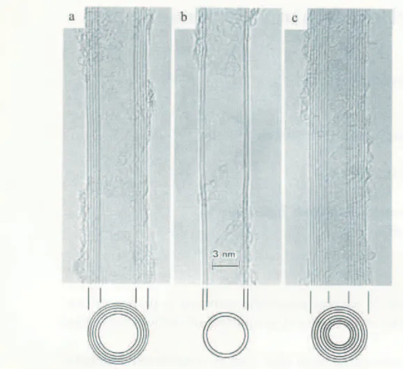
1.1 The observation by TEM of multi-wall coaxial nanotubes with var-ious inner and outer diameters, di and d0, and numbers of
cylin-drical shells N reported by Iijima in 1991: (a) N = 5, d0 = 67˚A;
(b) N = 2, d0 = 55˚A; and (c) N = 7, di = 23˚A, d0 = 65˚A.
(Reproduced from Ref. [1]) . . . 2
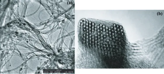
1.2 Images of carbon nanotubes, taken by a transmission electron mi-croscope (TEM) (reproduced from Ref. [6]). (a) An entangled web of nanotube ropes. The scale bar is 100 nm. (b) A cross section of a rope with many parallel nanotubes, packed in an ordered lattice. Each circle within the rope, with a diameter of about 1.4 nm, is a nanotube. The scale bar is 10 nm. . . 3
1.3 Image of the integral intensity of all Raman lines: Carbon nan-otubes assembled in rows with corresponding Raman spectra Scan range: 100 × 100 µm.(Samples were obtained from Prof. Tsukruk, Iowa State University,USA) . . . 4
1.4 An atomically resolved STM image of a chiral carbon nanotube (a) compared to a theoretical model of a nanotube with a similar chirality (b) The diameter of the tube is 1.2 nm.(Reproduced from [11, 15]) . . . 5
LIST OF FIGURES xx
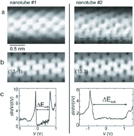
1.5 STM images and tunnel spectra for two different carbon nan-otubes. The 0.5-nm bar indicates the scale for all four images in (a) and (b). (a) Atomically resolved STM images of two nanotubes 1 and 2. (b) Two calculated images based on the (n,m) indices that are found for the nanotubes shown in (a). (b) Normalized dI/dV spectra for these nanotubes. Nanotube 1 appears to be semicon-ducting whereas nanotube 2 is metallic. Band edge separations ∆Esub are indicated for both curves. (Reproduced from Ref. [16]) 6
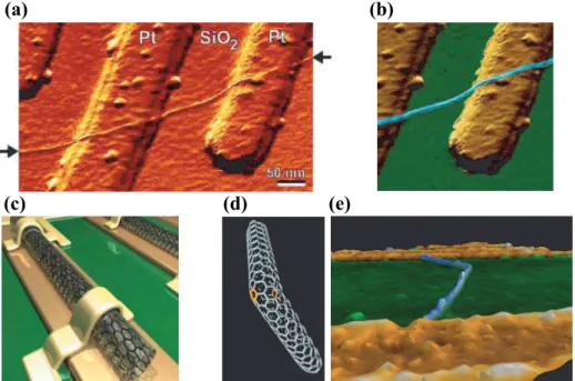
1.6 A nanotube as a molecular electronic wire on two microfabricated electrodes. By applying a bias voltage over the electrodes, a cur-rent can be measured through the molecule. (a)-(b) show nan-otube device. Pt electrodes used in this device. The electrode in the upper-left corner acts as a gate and can modulate the conduc-tance of the nanotube by applying an electric field. The scale bar is 50 nm. (c) Artistic figure of nanotube device used for transistor action. (c) Nanotube kinks. A theoretical model for a junction between two nanotubes with different chirality and similar diam-eter. Such a junction is possible when defect pairs of pentagons and heptagons are present in the hexagonal lattice. In this model the five-and seven-ring are opposite to each other in the kink. (b) A nanotube that contains a kink lying across electrodes. Such a sample layout allows to measure the electronic transport across a nanotube kink. The scale bar is 200 nm. (Reproduced from Ref. [17]) 7
2.1 Flow chart of VASP program. . . 54
3.1 Schematic experimental setup for the three common carbon nan-otube growth methods, (a) arc-discharge, (b) laser ablation (va-porization) and (c) chemical vapor deposition (CVD). . . 57
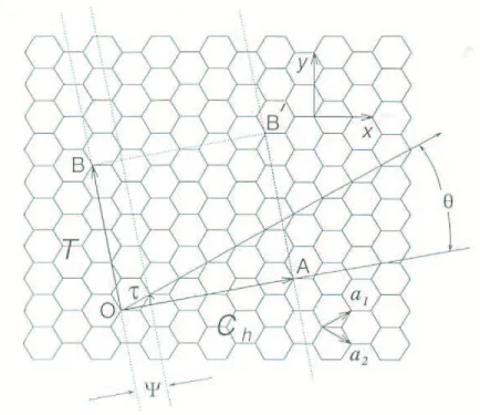
3.2 The 2D graphine sheet is shown along with the vector which speci-fies the chiral nanotube. The chiral vector OA or Ch = na1+ ma2
is defined on the honeycomb lattice by unit vectors a1 and a2 and
the chiral angle θ is defined with respect to the zigzag axis. Along the zigzag axis θ = 0o. Also shown are the lattice vector OB=T of
the 1D tubule unitcell, and the rotation angle ψ and the transla-tion τ which constitute the basic symmetry operatransla-tion R =< ψ|τ >. The diagram is constructed for (n, m)=(4, 2). Ref. [96] . . . 61
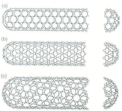
3.3 By rolling up a graphene sheet (a single layer of carbon atoms from a 3D graphite crystal) as a cylinder and capping each end of the cylinder with half of a fullerene molecule, a ”fullerene-derived tubule,” one layer in thickness, is formed. Shown here is a schematic theoretical model for a single-wall carbon tubule with the tubule axis OB (see. Fig. 3.2) normal to: (a) the θ = 30o
di-rection (an ”armchair” tubule), (b) θ = 0o(a ”zigzag” tubule), and
(c) a general direction B with 0 < |θ| < 30o (a ”chiral” tubule).
The actual tubules shown in the figure correspond to (n, m) values of (a)(5,5), (b)(9,0), and (c) (10,5). Ref. [96] . . . 62
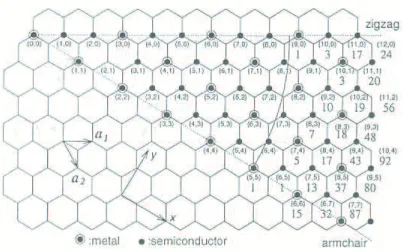
3.4 The 2D graphine sheet is shown along with the vector which spec-ifies the chiral nanotube. The pairs of integers (n, m) in the figure specify chiral vectors Ch (see table 3.1) for carbon nanotubes,
in-cluding zigzag, armchair, and chiral tubules. Below each pair of integers (n, m) is listed the number of distinct caps that can be joined continuously to the cylindrical carbon tubule denoted by (n, m). The circled dots denote metallic tubules and the small dots are for semiconducting tubules. Ref. [96] . . . 63
LIST OF FIGURES xxii
3.5 The relation between the fundamental symmetry vector R = pa1 + qa2 and the two vectors of the tubule unit cell for a
car-bon nanotube specified by (n, m) which, in turn, determine the chiral vector Ch and the translation vector T. The projection
of R on the Ch and T axes, respectively, yield ψ (or χ) and
τ . After (N/d) translations, R reaches a lattice point B′′. The
dashed vertical lines denote normals to the vector Ch at distances
of L/d, 2L/d, 3L/d, ..., L from the origin. Ref. [96] . . . 67
3.6 A hexagonal lattice with the lattice vectors a1 and a2, the grey
area corresponds to one choice of unit cell, rAand rB points to the
two atoms in the unit cell. . . 69
3.7 The figure shows the reciprocal lattice point and the Brillouin zone for graphene, with its high symmetry points. K and K′ are the
points where the π and π∗ dispersion bands is touching each other.
The three K points are equivalent since they are connected by the reciprocal lattice vectors b1 and b2. Since the points K and K′
cannot be connected by the reciprocal lattice vectors these point are not equivalent. . . 73
3.8 (a) Shows the dispersion relation for graphene, called the tent dis-persion. The points Γ, K, K′, M is high symmetry points and
their placement in the Brillouin zone can be seen in Figure 3.7, (b) is appeared by cutting (a) in straight lines between the points K → Γ → M → K . . . 74
3.9 An illustration of three Brillouin zones of graphene (gray areas) mutual displaced for clearance. The black lines shows allowed wave vectors for three different kinds of tubes (in all the cases some of the lines have been translated with reciprocal lattice vectors making them as close to symmetrical around Γ as possible). (a) shows the allowed states for a (10,10) tube. It can be seen that it is metallic since one of the lines go through the K and K′ points. (b) shows
the allowed states for a (12,0) tube which is also metallic. (c) is the same figure for a (11,0) tube and it can be seen that it is semiconducting since none of the lines go through the K and K′
points. . . 76
3.10 Band diagram of dispersion relation for three different tubes (a) is a metallic (10,10) tube, the inset is zoom-in of the bands touching the Fermi surfaces −0.95 < k < 0.75. (b) is a metallic (15,0) tube the inset is again a zoom-in around k = 0. (c) is semiconducting (12,8) tube. Due to the huge unit cell there are a lot of bands. Left inset is energy zoom-in where k is in the same range as in the big plot. The right inset is a zoom-in energy and around k=0 showing the band gap.(Reproduced from Ref. [101]) . . . 77
3.11 Inset: A schematic side view of a zigzag SWNT, indicating two types of C–C bonds and C–C–C bond angles. These are labelled as d1, d2, θ1 and θ2. (a) Normalized bond lengths (d1/d0 and d2/d0)
versus the tube radius R. (d0 = 1.41 ˚A). (b) The bond angles (θ1
and θ2) versus R. (c) The curvature energy, Ecur per carbon atom
with respect to graphene as a function of tube radius. The solid lines are the fit to the data as α/R2. (Reproduced from Ref. [105]) 80
LIST OF FIGURES xxiv
3.12 (a) Energies of the double degenerate π–states (VB), the double degenerate π∗–states (CB) and the singlet π∗–state as a function of
nanotube radius. Each data point corresponds to n ranging from 4 to 15 consecutively. (b) The calculated band gaps of Ref. [105] are shown by filled symbols. Solid (dashed) lines are the plots of Eq. 3.23 (Eq. 3.22). The experimental data taken from [15, 104, 116] are shown by open diamonds. (Reproduced from Ref. [105]) . 82
3.13 The energy band diagram (left) and density of states (right) for a metallic (top) and a semiconducting (bottom) nanotube. The energy dispersion diagrams are calculated with Eqs. (2.4) and (2.5) for a (5,5) and (10,0) nanotube respectively. The energy is divided by the energy overlap integral γ0 = 2.9 eV. In the density
of states (DOS) diagrams a series of sharp peaks appear which are the subband onsets. The energy differences between the first two singularities near the Fermi level are indicated for the metallic and the semiconducting case by ∆Esub and ∆Egap respectively. . . 85
3.14 Shows the electrostatic potential through a metallic carbon nan-otube measured with Electrostatic Force Microscopy (EFM). It can be seen that the potential is constant corresponding to very low intrinsic resistance indicating that the tube is ballistic. From [140]. 90
3.15 Illustrates a simple model for the system that we are looking at . 92
3.16 (a) The strain component ǫxx = (R0− a)/R0 along the major axis
as a function of applied strain ǫyy = (R0− b)/R0 along the minor
axis. The slope is the in-plane Poisson ratio, νk. (b) Variation of the elastic deformation energy per carbon atom, (c) The restoring force on fixed carbon atoms. For (8, 0) SWNT, the force is scaled by 0.5 since it is only on one carbon atom, while for the other tubes it is on two carbon atoms. (Reproduced from Ref. [131]). . . 95
3.17 (a) The variation of the band gap, Eg. (b) Density of states at the
Fermi level D(EF) as a function of applied strain ǫyy. (Reproduced
from Ref. [131]). . . 97
3.18 The variation of energy eigenvalues of states near the band gap at the Γ–point of the BZ as a function of the applied strain. The shaded region is the valance band. The singlet state originating in the conduction band is indicated by squares. (Reproduced from Ref. [131]). . . 99
3.19 Binding energies Eb of single hydrogen and aluminum atom
ad-sorbed on the zigzag SWNTs versus the radius of the tube R. The solid line is the fit to the Eb,A(R) = Eo,A+ CA/R explained in the
text. (Reproduced from Ref. [113]). . . 101
3.20 (a) Variation of the binding energies Eb of single hydrogen atom
adsorbed on a (8,0) zigzag SWNT as a function of the radial de-formation ǫyy defined in the text. The upper curve corresponds to
H adsorbed on the high curvature site of the deformed tube. The lower curve is for the adsorption on the low curvature site. (b) Same as (a) for a single Al atom. (Reproduced from Ref. [113]). . 103
3.21 Optimized structures of SWNT ropes.(a) (6, 0), (b) (7, 0) nan-otubes are packed by VdW interaction under zero pressure, and (c) (7, 0) one-dimensional interlinked under pressure. The inter-linked structure in (c) has lower total energy than VdW packed structure in (b). Lattice parameters of the ropes, a, b, and c, and γ angle are shown. (Reproduced from Ref. [154]). . . 105
3.22 Total energy versus 2D lattice constant of (7, 0) nanotube ropes in different phases. The top view along the axis of the rope of the different phases are shown by inset. The zero of energy is set to the total energy calculated for the optimized structure of VdW packed rope at zero pressure. (Reproduced from Ref. [154]). . . 106
LIST OF FIGURES xxvi
3.23 Two-dimensional crystal structure and relevant physical parame-ters for various high-density phases of carbon nanotubes. (a)2D interlinked structure of (5, 0) nanotubes. (b) A hexagonal network of (9, 0) nanotubes, in which (9, 0) tubes are interlinked along a, b, and [110] directions. (c) A very dense structure of (7, 0) nan-otubes obtained under 30 GPa. (d) The optimized structure of (6, 6) armchair tubes under 53 GPa. Nanotubes are distorted in such a fashion that the local nearest-neighbor structure is reminis-cent of the graphite. dC−C indicates the smallest distance between two carbon atoms of nearest-neighbor tubes in the rope. (Repro-duced from Ref. [154]). . . 108
4.1 Schematic description of the physisorption sites of O2 molecule
on the (8, 0) SWNT. Geometrical data and binding energies corre-sponding to these sites are given in Table 4.1. The GGA optimized distance from one O atom of the molecule to the nearest C atom of SWNT is denoted by dC−O. Es is the GGA chemical bonding
energy for spin-polarized triplet state. Eb is the binding energy
including the van der Waals interaction. . . 114
4.2 Schematic description of the various adsorption sites of atomic O on the (8, 0) SWNT. Some relevant geometrical data and GGA chemical bond (chemisorption) energies, corresponding to these sites are also given. Es: chemisorption energy; dC−O: length of
the C–O bond; dC−C: length of the C–C bond under adsorbed O atom. Es is obtained from the spin-unpolarized calculations of the
total energies in Eq. 4.1. . . 120
4.3 Charge density contour plots on a plane containing O atom and nearest C–C bond in the case of a-site chemisorption (a) and z-site chemisorption (b). These chemisorption z-sites and their atomic configuration are described as insets. . . 123
4.4 (a) Spin unpolarized energy bands of the (8, 0) bare s-SWNT; (b) spin polarized (dashed lines) and spin unpolarized (solid lines) en-ergy bands of the linear O2 chain with the same lattice parameter
c; (c) spin unpolarized energy bands of the O2 physisorbed on the
(8, 0) tube with Oppπ∗ state pinning the Fermi level. (d)
Spin-polarized bands corresponding to (c). Zero of energy is taken at the Fermi level shown by dash-dotted line. Up-spin and down-spin bands are indicated by corresponding arrows. Here csc = c. . . 124
4.5 Spin unpolarized and spin polarized bands of O2 physisorbed on
different sites of (8, 0). calculations are performed by using dou-ble cells. The adsorption sites are shown by insets. (a) Spin-unpolarized and (e) triplet state bands for A-site physisorption. The total density of states with thin and dashed lines, and par-tial density of states of adsorbed O2 with thick lines are presented
in panel (e). The zero of energy is taken at the Fermi level in-dicated by dash-dotted lines. (b) spin-unpolarized and (f) triplet state bands for H-site. (c) and (g) are same for T-site; (d) and (h) for Z-site. For the triplet state in left panels, the spin-up and spin-down bands are shown by dashed and thin lines . . . 126
4.6 (a) Spin polarized electronic energy band structure of the zigzag chain of O2 adsorbed above the adjacent axial C-C bonds along
the axis of a (8, 0) s-SWNT as shown by inset. Solid and dashed lines are the spin-down and spin-up bands. The zero of energy is taken at the Fermi level EF indicated by dash-dotted line. (b)
Corresponding total density of states of s-SWNT+O2 and
par-tial density of states on the oxygen atoms are shown by solid and dashed lines. (c) Band structure of the row of O2 physisorbed at
T-sites as shown by inset. (d) Same as (b). . . 129
4.7 Energy band structures of O2 physisorbed on the (6,6) armchair
SWNT. (a) B-site, (b) H-site. Spin-up and spin-down bands are shown by broken and continuous lines. . . 130
LIST OF FIGURES xxviii
4.8 (a)Variation of the percentage values of C/Co
(ET/ETo;
dO−O/do
O−O; µ/µo; and Eg/Ego) with the O2-SWNT separation d.
Eo
T, doO−O, µo and Ego corresponds to the stable physisorption state
with do = 2.89 ˚A at the A-site. (b) The total energies of the
sin-glet bound states found at small d at Z-site (square) and at the A-site (diamond). The total energy of the triplet ground state cor-responding to the physisorption state for the Z- and A- sites at d ∼ 2.9˚A are shown by continuous and broken lines. . . 131
4.9 Variation of the total energy, ET; force acting on the O2 molecule,
F⊥; bond distance of O2, dO−O; and magnetic moment, µ with O2
-(6,6) SWNT distance d for O2 adsorbed on the H-site of the (6,6)
SWNT. Calculations have been performed in the double-cell. . . . 133
5.1 A schematic description of different binding sites of individual atoms adsorbed on a zigzag (8,0) tube. H: hollow; A: axial; Z: zigzag; T: top; S: substitution sites. . . 137
5.2 Variation of the calculated spin-unpolarized Eu
b and spin-polarized
Ebp binding energy of transition metal atoms with respect to the number of d-electrons Nd. The bulk cohesive energy Ec and the
bulk modulus B from Ref. [75] is included for the comparison of the trends. . . 142
5.3 Energy band structures and total density of states (TDOS) of bare tubes with fully relaxed atomic structure. (a) Electronic structure of the semiconducting (8,0) zigzag SWNT calculated for the dou-ble primitive unit cells consisting of 64 C atoms. (b) same for the metallic (6,6) armchair SWNT calculated for the quadruple prim-itive unit cells including 96 C atoms. Zero of energy is set at the Fermi level EF. . . 144
5.4 Energy band structures and total density of states (TDOS) of sin-gle Au, Mn, Mo, and Ti adsorbed on a zigzag (8,0) tube. Zero of energy is set at the Fermi level. Bands and state density of spin-up and spin-down states are shown by dotted and continuous lines, respectively. Mn, Mo, Ti are adsorbed at the H-site; and Au is adsorbed at the T-site. . . 145
6.1 (a) Fully optimized atomic structure of Ti covered (8,0) SWNT. (b) The cross section with different types of C atoms (identified as C1, C2, and C3) and adsorbed Ti atoms (Ti1, Ti2 and Ti3). Dark-small and light-large circles indicate C and Ti atoms, respec-tively. (c) Histograms show the variation of bond-lengths of differ-ent carbon-carbon (dC−C), carbon-Ti (dC−T i) and Ti-Ti (dT i−T i) bonds. . . 151
6.2 (a) Electronic energy band structure of a Ti covered (8,0) SWNT. (b) The total density of states (TDOS). TDOS of bare (8,0) tube is shown by dashed lines. Zero of energy is taken at the Fermi level.151
6.3 Calculated state densities.(a) Local density of states (LDOS) on C1, C2, C3 atoms of carbon nanotube which has the same atomic configuration and square-like cross section as the carbon nanotube covered by Ti as shown in Fig. 6.1. See inset. (b) LDOS on the carbon atoms of the Ti covered SWNT (i.e. C1+C2+C3). (c) LDOS calculated on the Ti atoms of the Ti covered SWNT (i.e. Ti1+Ti2+Ti3). Partial density of states of s-, p-, and d-orbitals are also shown. . . 154
6.4 Fully optimized atomic structures of Ti, Co, Cr, Fe, Mo covered (8,0) SWNT. . . 156
6.5 Optimized atomic structures of Ti covered: (a) (8,0) SWNT (C32Ti16); (b) (9,0) SWNT (C36Ti18); (c) (6,6) SWNT (C24Ti12). 158
LIST OF FIGURES xxx
6.6 Optimized atomic structure of (8,0) and (9,0) zigzag, and (6,6) armchair SWNT which are uniform covered with Ti. Correspond-ing density of states for spin-up and spin-down electrons are shown. 159
6.7 (a) Fully optimized atomic structure and square-like cross section of Ti coated (8,0) zigzag SWNT including 16 Ti atoms per unit cell (C32Ti16). Ti and C atoms are indicated by large-light and
small-dark circles. (b) Spin-polarized band structure of C32Ti16 at
ǫzz = 0 with the Fermi level set to zero of energy. Majority spin,
En(k ↑) and minority spin, En(k ↓) bands are shown by continuous
and dotted lines, respectively. Spin polarized density of states for majority D↑(E) and minority D↓(E) spin states. (d) Fully
optimized atomic structure of Ti covered (8,0) SWNT including four additional Ti atoms adsorbed at the corners of the square-like tube (i.e. C32Ti24). (e) and (d) show corresponding spin-polarized
band structure and DOS, respectively. Nearest Ti atoms to the four additional adsorbed Ti atoms are indicated by nnTi. . . 161
6.8 Top Inset: side view of the Ti covered (8,0) SWNT (i.e. C32Ti16)
strained along its axis. ǫzz > 0 corresponds to the stretched
struc-ture with c > c0. (a) Variation of the magnetic moment µ per unit
cell of C32Ti16 as a function of the lattice parameter c or strain.
(b) Calculated axial stress in the system as a function of c. (c) Variation of the total energy E with c. The minimum of E oc-curs at c0 = 4.17 ˚A. Insets in (c) show the distribution of Ti-Ti
bond-lengths corresponding to c0 = 4.17 ˚A and c = 4.34 ˚A. . . 163
6.9 Calculated spin-polarized band structure of C32Ti16 under ǫzz =
0.04 at c = 4.34 ˚A. En(k ↑) and En(k ↓) are shown by continuous
and dotted lines, respectively. Corresponding densities of majority and minority spin states are shown in the panel on the right hand side. . . 165
6.10 Densities of majority and minority spin states of C32Ti showing
curvature effect on P (E). (a) Density of spin states for a single Ti atom adsorbed on a bare (8,0) SWNT. (b) Density of states for a single Ti atom adsorbed on the high curvature site of (8,0) SWNT under radial deformation ǫyy = 0.3, which transforms the circular
cross section to an elliptical one as shown by insets. . . 166
7.1 (a) Supercell used to simulate a junction of two crossed tubes. Fp(D) is the contact force generated due to a fixed distance
D < DV dW, and s(D) is optimized spacing between the surfaces of
two SWNTs at the contact. (b) Bridge-Hollow (B-H) atomic reg-istry between two parallel zigzag SWNT, where the C-C bonds of top SWNT along its axis face the hexagon of the bottom SWNT. (c) Same as (b) for the crossbar structure. (d) Hexagon-Hexagon (H-H) atomic registry for the crossbar structure. The lattice pa-rameter of the bare (8,0) tube is cSW N T = 4.25 ˚A. . . 174
7.2 Relaxed atomic structures of two crossed (8, 0) SWNTs with dif-ferent atomic registries (H-H and B-H). B-H junction has been studied for five different spacing values of s(D) labelled by B-H1, B-H2, B-H3, B-H4, and B-H5. . . 175
7.3 (a) Variation of relaxed spacing s, between two crossed nanotubes and (b) its energy (shown by diamonds) and contact force Fp
(shown by triangles) as a function of D. The stress per super-cell and atomic configuration of the junction are shown by insets. In (a) filled circles, light diamond and triangle indicate B-H, H-H registries and B-H registry including single vacancy, respectively. In (b) diamonds and triangles are joined by lines as a guide to the eye; but the detailed structure of possible local minima are omitted.176
LIST OF FIGURES xxxii
7.4 Contour plots of total charge density ρT and SCF electronic
po-tential Ve of B-H2 and B-H3 junctions. In the right panels the
potential energy in the white regions is higher than the Fermi en-ergy, ie. ΦB > 0. . . 177
7.5 Relaxed atomic structure, total charge density ρT and
SCF-electronic potential Ve of junction of crossed SWNTs. Left panels:
B-H5 contact; right panels: B-H5 type contact including a single carbon vacancy. (a) and (b) are charge density contour plots on a lateral plane bisecting the spacing s between tubes. (c) and (d) are the same for electronic potential energy. While Ve> EF at the
contact and hence ΦB > 0 in (c), the potential barrier is collapsed
and an orifice is formed between two tubes through the contact in (d). . . 180
7.6 Relaxed atomic structure of the junctions between two parallel tubes under different contact force or D. (a) Large D and hence weak deformation. (b) Small D hence strong deformation. (c) Relaxed junction after the contact force in (b) is released. Parallel tubes have B-H registry. . . 182
7.7 Relaxed atomic structure of a junction B-H2 after the contact forces Fp are released. . . 183
7.8 Energy band structure along the z-axis shown by inset, and relaxed atomic structure of the corresponding 3D grid of the (8, 0) zigzag tubes. . . 185
7.9 An atomistic model which describes the electronic transport through the junction. L and R are reservoirs where finite tubes forming the junction are coupled to. . . 186
7.10 Calculated conductance G versus energy E for various junctions. (a) Distribution ordering of interatomic distances in the B-H2 junc-tion i.e. Rij versus number index of sorted distances. Dashed line
at 1.75 ˚A and 2.91 ˚A correspond to the domains of tight-binding parametrization; (b) B-B junction of two parallel tubes connected by a carbon atom; (c) B-H2 junction of crossed tubes. (d) B-H2 junction relaxed after contact forces are released; (e) B-H3 junc-tion; (f) B-H4 juncjunc-tion; (g) Junction having H-H registry; (h) B-H6 junction which is B-H5 including a single vacancy. In all plots cou-pling parameter is fixed at γ = 0.5. Zero of energy is set at the Fermi level. . . 188
7.11 (a) LDOS at different Au and C atoms of the (8,0) zigzag SWNT side bonded to the Au(100) surface. The location of atoms are described by inset. The zero of energy is taken at the Fermi energy EF. State densities shown by empty circle and filled diamonds
correspond to 6 neighboring carbon atoms. Other densities are for single atoms. (b) Contour plots of the SCF electronic potential, Ve(r), on a vertical plane. (c) Same as in (b) on a horizontal plane
bisecting s. In the dark gray regions Ve(r) > EF. (d), (e) and (f)
correspond to the radially deformed (8,0) SWNT pressed between two 3-layer Au(100) slabs with b/a = 0.47 as shown by inset. State densities shown by empty circles in (d) correspond to 6 neighboring carbon atoms. Other densities are for single atoms. (g) Variation of Ve(z) on a perpendicular line passing through the center of SWNT.193
LIST OF FIGURES xxxiv
7.12 (a) LDOS at different Mo and C atoms of the (8,0) zigzag SWNT side bonded to the Mo(110) surface. The location of atoms are described by inset. The zero of energy is taken at the EF. State
densities shown by empty circles and filled diamond correspond to 8 neighboring carbon atoms, Others are for single atoms. (b) Contour plots of the total SCF charge density on a vertical plane. (c) Difference charge density showing the charge depleted (white) regions and charge accumulate (black) regions. (d) LDOS corre-sponding to the (8,0) SWNT radially deformed between two 3-layer Mo(110) slabs with b/a = 0.56 as shown by the inset. State densi-ties shown by empty circles correspond to 10 neighboring carbon atoms. . . 195
8.1 Variation of chemical interaction energy EC between SWNT and
H2 molecule as a function of distance d between them. Two cases,
namely adsorption to bare and radially deformed SWNT are shown by dashed and continuous lines, respectively. In calculating both curves, atomic structures corresponding to d → ∞ have been used without relaxation. Dash-dotted line indicate zero of chemical in-teraction energy. Optimized distance for two cases are indicated by arrows. . . 200
8.2 Atomic configuration, energy band structure and LDOS calculated for the coadsorption of H2 molecule and single Li atom. Two cases
correspond to Li atom chemisorbed on the external and internal surface of the (8,0) zigzag SWNT. Zero of energy is set at the Fermi level, EF. LDOS calculated at Li and H2 are shown by
continuous and dotted lines, respectively. Metallized SWNT bands are indicated by arrows. . . 203
8.3 (a) Atomic configurations for single, double and triple Pt atoms adsorbed on the (8,0) SWNT. Average binding energy of adsorbed Pt atoms Eb and bond distances are indicated. . . 206
8.4 Optimized binding configuration of H2molecules adsorbed to a free
Pt atom. (a) Dissociative adsorption of a single H2 molecule. (b)
The first H2 is dissociatively, second H2 molecularly adsorbed. (c)
Two H2are molecularly adsorbed. (d) Two H2are molecularly, one
H2 dissociatively adsorbed (e) Four different configurations related
with the adsorption of two H2 to the same free Pt atom. Binding
energy of the nth H
2 molecule adsorbed to Pt atom, Eb(n); average
binding energy per H2, Eb, total energy with respect to constituent
atoms ET and bond distances are indicated. . . 207
8.5 Optimized geometry for a single H2 molecule adsorbed to a single
Pt atom. (a) Pt atom is adsorbed near the H-site of (8,0) SWNT (side and top view) (b) Pt at the A-site (bridge position) of (8,0) SWNT (side and top view) (c) Pt atom is adsorbed near the H-site of the graphite surface (d) Pt atom at the A-site of graphite. ET is
the total energy relative to the constituent free C, Pt and H atoms. 209
8.6 Optimized structure of H2 molecules adsorbed to the Pt atom on
the SWNT. (a) One H2 adsorbed to PtH2. The inset show the
regions of charge depletion (∆ρ < 0) and charge accumulation (∆ρ > 0) as a result of the bonding between SWNT and PtH2+H2
in (a). (b) Another local minima where two H2 is molecularly
adsorbed to the Pt atom. (c) One H2 is chemisorbed two H2 are
weakly bound. (d) four H2. . . 211
8.7 Dissociative adsorption of single H2 on a small Pt cluster adsorbed
on SWNT (a). One H2 is approaching two adjacent Pt atoms
adsorbed on SWNT. (b) Optimized geometry after dissociative adsorption of H2. (c) Variation of total energy with distance z.
Dashed curve corresponds to ET for unrelaxed H2 and unrelaxed
SWNT. Continuous curve corresponds to ET of the geometry
re-laxed at certain values of z. (d), (e) and (f) same as (a), (b) and (c) except the Pt cluster consists of 3 Pt atoms. z is the distance from the surface of SWNT. Variation of ET(z) is amplified by inset. 213
List of Tables
2.1 Calculated and experimental values of cohesive energies, Ec, lattice
constants, c and energy gaps, Eg for Si crystal by using LDA,
func-tionals of GGA; Langreth-Mehl (LM), Perdew-Wang 86 (PW86), Perdew-Wang 91 (PW91), Perdew-Becke (B88), Perdew-Burke-Ernzerhof (PBE). . . 40
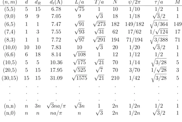
3.1 Parameters of carbon nanotubes Ref. [96] . . . 64
3.2 Values for characterization parameters for selected carbon nan-otubes labelled by (n, m) Ref. [96] . . . 65
3.3 Character table for group D(2j+1). Ref. [96] . . . 66
3.4 Character table for group D(2j+1). Ref. [96] . . . 66
3.5 Basis functions for groups D(2j) and D(2j+1). Ref. [96] . . . 67
3.6 Band gap, Eg, as a function of radius R of (n,0) zigzag nanotubes.
M denotes the metallic state. First row values were obtained within GGA in Ref. [105] Second and third rows from Ref. [118] are LDA results, while all the rest are tight-binding (TB) results. Two rows of Ref. [128] are for two different TB parametrizations. . . 81
3.7 In–plane elastic constants of SWNTs. All elastic constants are in GPa except for νk which is unitless. Cef f = C11(1 −
ν2
k).(Reproduced from Ref.[131]) . . . 98
4.1 Calculated binding energies, Eb, of O2 molecule at different sites of
the (8, 0) SWNT. Different sites of physisorption, A-, H-, Z-, and T-sites, are described in Fig 4.1. Calculation of GGA chemical bonding energies, Es are performed by using single (i.e. csc = c)
and double (i.e. csc = 2c) supercells. In the third column u, s, and
t indicate spin-unpolarized, spin-polarized singlet state and triplet calculations, respectively. The GGA optimized distance from one O atom of the molecule to the nearest C atom of SWNT is denoted by dC−O. The average bond length of O2 is 1.24 ˚A. The GGA
chemical bonding energies Es exclude the O2–O2 coupling energy
except one given in the parenthesis. The binding energies, Eb in
the sixth column includes the van der Waals interactions. . . 116
4.2 Calculated C–O distance dC−O, chemical bonding energy Es, van
der Waals energy EV dW, and binding energy Eb for O2 physisorbed
on the H-, and B-site of (6, 6) armchair m-SWNT. . . 118
4.3 Calculated chemical bonding energies of chemisorbed O atom at a-site and z-site. For Est
s and Esss the ground state for the oxygen
chemisorbed SWNT is the singlet state, but isolated O atom (refer-ence state) is in the triplet state and the singlet state, respectively. Estt corresponds to the both isolated O and O chemisorbed SWNT
in the triplet state. Eu
s stands for spin-unpolarized calculation.
LIST OF TABLES xxxviii
5.1 Calculated binding energies and average carbon-adatom bond dis-tances, ¯dC−A of individual atoms adsorbed at H-, Z-, A-, and T-sites of the (8,0) SWNT as described in Fig. 6.1. Binding energies, Eu
b are obtained from spin-unpolarized total energies calculated for
fully relaxed atomic structure. . →H implies that the adatom at the given site is not stable and eventually it moves to the H-site. . 139
5.2 Calculated binding energies and average carbon-adatom bond dis-tances, ¯dC−A of individual atoms adsorbed at H-, Z-, A-, and T-sites of the (6,6) SWNT as described in Fig. 6.1. Binding energies, Ebuare obtained from spin-unpolarized total energies calculated for
fully relaxed atomic structure. . . 139
5.3 Strongest binding site (as described in Fig. 6.1); adsorbate-C dis-tance ¯dC−A; the difference between unpolarized and spin-polarized total energies ∆ET; binding energy Ebu obtained from
spin-unpolarized calculations; binding energy Ebp obtained from spin-polarized calculations; magnetic moment (µB per supercell)
of the magnetic ground state corresponding to the adsorption of various individual atoms on the (8,0) SWNT. . . 140
5.4 Strongest binding site (as described in Fig. 6.1); adsorbate-C dis-tance ¯dC−A; the difference between unpolarized and spin-polarized total energies ∆ET; binding energy Ebu obtained from
spin-unpolarized calculations; binding energy Ebp obtained from spin-polarized calculations; magnetic moment µ per supercell cor-responding to the magnetic ground state corcor-responding to the ad-sorption of individual Ti, Mn, Mo, Au atoms on a (6,6) SWNT. . 140
Introduction
Miniaturization is the act of making things on a greatly reduced scale. Nan-otechnology is a giant step toward miniaturization. The smaller the wires and switches on silicon chips that run everything from toys to supercomputers, the more efficient and less expensive these things become. Since 1960s the number of switches and other elements on a finger-nail size chip has doubled every 18 months from dozens to tens of millions. The new field of science, nanotechnology, can now provide wires with diameters a scant few hundreds of millionths of an inch in diameter, a hundred or so atoms across. Why these state of the art wires are so important for nanoelectronics?
Scientists had in fact been looking for many years for a suitable molecule to use as a miniscule electrical wire. In a bottom-up strategy proposed to design ultra-small electronic circuits, individual atoms and molecules could be building blocks for the construction of devices. However, the fabrication of a single molecule de-vice proved to be experimentally challenging because of the difficulty to achieve electrical contacts to molecules. In 1991, reported observation about this kind of molecules, ”Carbon Nanotubes”, was done by Iijima[1]. In his first observation he found multi-wall nanotubes (Figure 1.1). It took, however, less than two years before single-wall carbon nanotubes (SWNTs) were discovered experimentally by also Iijima[2] at the NEC Research Laboratory in Japan and by Bethune[3] at the IBM Almaden Laboratory in California. These experimental discoveries and
CHAPTER 1. INTRODUCTION 2
Figure 1.1: The observation by TEM of multi-wall coaxial nanotubes with various inner and outer diameters, di and d0, and numbers of cylindrical shells N reported
by Iijima in 1991: (a) N = 5, d0 = 67˚A; (b) N = 2, d0 = 55˚A; and (c) N = 7,
di = 23˚A, d0 = 65˚A. (Reproduced from Ref. [1])
the theoretical work, which predicted many remarkable properties of carbon nan-otubes, launched this field and propelled it forward. The field has been advancing at a rapid pace ever since leading many interesting discoveries. Carbon nanotubes were soon recognized as ideal candidates for nanotechnology. They are robust, flexible and long enough to connect two microfabricated devices[4, 5]. Above all, they can be well-conducting. It took a few years however, until 1995, before it became possible to produce clean carbon nanotubes consisting of only one shell in large, practical quantities[6].
(a)
(b)
Figure 1.2: Images of carbon nanotubes, taken by a transmission electron mi-croscope (TEM) (reproduced from Ref. [6]). (a) An entangled web of nanotube ropes. The scale bar is 100 nm. (b) A cross section of a rope with many paral-lel nanotubes, packed in an ordered lattice. Each circle within the rope, with a diameter of about 1.4 nm, is a nanotube. The scale bar is 10 nm.
electronic and mechanical properties[4, 5], so stemming from the close relation between carbon nanotubes and graphite, and some from their one-dimensional aspects. Initially, carbon nanotubes aroused great interest in the research community because of their exotic electronic structure. As other intriguing properties have been discovered, such as their remarkable electronic transport properties[7, 8, 9, 10, 11, 12, 13, 14], their unique Raman spectra[5] (figure 1.3), and their unusual mechanical properties, interest has grown in their potential use in nanometer-sized electronics and in a variety of other applications.
Carbon nanotubes can be semiconducting or metallic which depends on two parameters, the diameter and the chiral winding of the carbon network along the tube shell. Although this prediction was already made in 1992, it was confirmed experimentally only six years later by scanning tunnelling microscopy (STM) measurements[11, 15]. STM proved to be a useful technique to study nanotubes since it has the power to reveal both the atomic and electronic structure. It is possible to obtain beautiful images of atomically resolved nanotubes from which their chiralities can be obtained. An example is shown for example in Figure 1.4 together with a theoretical model of a nanotube with a comparable chirality. The tip of an STM can also be used as a spectroscopic probe by keeping the tip fixed
CHAPTER 1. INTRODUCTION 4
Figure 1.3: Image of the integral intensity of all Raman lines: Carbon nanotubes assembled in rows with corresponding Raman spectra Scan range: 100 × 100 µm.(Samples were obtained from Prof. Tsukruk, Iowa State University,USA)
(a)
(b)
Figure 1.4: An atomically resolved STM image of a chiral carbon nanotube (a) compared to a theoretical model of a nanotube with a similar chirality (b) The diameter of the tube is 1.2 nm.(Reproduced from [11, 15])
above the sample and measure the tunnel current as a function of the bias voltage. By taking current-voltage spectra on a large number of nanotubes with various chiralities, two classes of nanotubes could be identified[16] (Figure 1.5). The STM spectra for these two classes corresponded remarkably well to the predicted electronic density of states (DOS) for the metallic and the semiconducting type, respectively. Due to the quantization of available energy modes in the circumfer-ential direction the DOS for nanotubes does not consist of one smooth band but it splits up into several subbands with sharp singularities at the onsets. These subbands represent separate one-dimensional channels for conduction along the nanotube [16]. The subbands and their sharp onsets were indeed observed in the tunnelling DOS that was obtained from the STM spectroscopy measurements[16].
Both the semiconducting and metallic types of nanotubes may be of use for nanoscale electronic devices (Figure 1.6(a,b,c)). Junctions between two differ-ent nanotubes that have a differdiffer-ent electronic character are interesting as well. Theoretical calculations have shown that two nanotubes with different chirality and similar diameter can connect to each other when defect pairs of five- and seven-rings of carbon are present in the hexagonal carbon lattice [18]. The con-nections appear as sharp kinks (Figure 1.6d) which have been also observed in real nanotube material. Figure 1.6e shows for example a sharply kinked nanotube
CHAPTER 1. INTRODUCTION 6
Figure 1.5: STM images and tunnel spectra for two different carbon nanotubes. The 0.5-nm bar indicates the scale for all four images in (a) and (b). (a) Atomi-cally resolved STM images of two nanotubes 1 and 2. (b) Two calculated images based on the (n,m) indices that are found for the nanotubes shown in (a). (b) Normalized dI/dV spectra for these nanotubes. Nanotube 1 appears to be semi-conducting whereas nanotube 2 is metallic. Band edge separations ∆Esub are
(a) (b)
(c) (d) (e)
Figure 1.6: A nanotube as a molecular electronic wire on two microfabricated electrodes. By applying a bias voltage over the electrodes, a current can be measured through the molecule. (a)-(b) show nanotube device. Pt electrodes used in this device. The electrode in the upper-left corner acts as a gate and can modulate the conductance of the nanotube by applying an electric field. The scale bar is 50 nm. (c) Artistic figure of nanotube device used for transistor action. (c) Nanotube kinks. A theoretical model for a junction between two nanotubes with different chirality and similar diameter. Such a junction is possible when defect pairs of pentagons and heptagons are present in the hexagonal lattice. In this model the five-and seven-ring are opposite to each other in the kink. (b) A nanotube that contains a kink lying across electrodes. Such a sample layout allows to measure the electronic transport across a nanotube kink. The scale bar is 200 nm. (Reproduced from Ref. [17])
CHAPTER 1. INTRODUCTION 8
lying across electrodes. Recent electronic transport measurements on this type of sample indicate that these kinks can indeed be semiconductor-metal junctions [19]. The mechanical properties of carbon nanotubes are also of large interest to scientists. Nanotubes have extremely high Young modulus. When they are strongly bent, they do not break but buckle. When the bending strain is released, nanotubes come back to its original position.
1.0.1
Historical Introduction
Very small diameter (less then 10 nm) carbon filaments were prepared in the 1970’s and 1980’s through the synthesis of vapor grown carbon fibers by the de-composition of hydrocarbons at high temperatures in the presence of transition metal catalyst particles of < 10 nm diameter. However, no detailed systematic studies of such very thin filaments were reported in these early years. It was the Iijima’s observation of the multiwall carbon nanotubes in Fig. 1.1 in 1991 that heralded the entry of many scientists into the field of carbon nanotubes, stimu-lated at first by the remarkable 1D quantum effects predicted for their electronic properties, and subsequently by the promise that the remarkable structure and properties of carbon nanotubes might give rise to some unique applications. The most striking of these theoretical developments was the prediction that carbon nanotubes could be either semiconducting or metallic depending on their geomet-rical characteristics, namely their diameter and the orientation of their hexagons with respect to the nanotube axis. Though predicted in 1992, it was not until 1998 that these predictions regarding their remarkable electronic properties were corroborated experimentally.
A major breakthrough occurred in 1996 when Smalley[6] and coworkers at Rice university successfully synthesized bundles of aligned single wall carbon nan-otubes, with a small diameter distribution, thereby making it possible to carry out many sensitive experiments relevant to 1D quantum physics, which could not previously be undertaken. Of course, actual carbon nanotubes have finite length, contain defects, and interact with other nanotubes or with the substrate and these factors often complicate their behavior.
In 1997, Dekker[21] and his coworkers made first step to use nanotubes as a nanodevices. They made electrical contacts to carbon nanotubes so that a large array of electrodes have been fabricated with conventional electron beam lithogra-phy, metal-evaporation and lift-off. They investigated the quantum conductance of SWNT. Also in this year carbon nanotubes dealt with as a hydrogen storage de-vice. Bethune et al.[22] proposed that SWNT can be used as a potential hydrogen storage. In 1998, aligned SWNT synthesized by using chemical vapor deposition technique[23]. At that year nanotube peapods synthesized[24]. In 2000, unusual high thermal conductivity observed in nanotubes[25]. The thermal conductiv-ity of both SWNTs and MWNTs should reflect the on-tube phonon structure, regardless of tube-tube coupling. Measurements of the thermal conductivity of bulk samples show graphite-like behavior for MWNTs but quite different behav-ior for SWNTs, specifically a linear temperature dependence at low T which is consistent with one-dimensional phonons.
In 2001, integration of SWNT for logic circuits achieved[26]. Nanotubes cir-cuits using electrical breakdown obtained by Collins et al.[26] At that time su-perconductivity observed in nanotubes[27].
1.1
Functionalization of carbon nanotubes
With their remarkable physical, electronic, and chemical properties, they are potential materials for their use in various applications ranging from reinforced fibers and nanocomposites to field-emission devices to capability of hydrogen storage. However, many of these applications require modifications to the pris-tine nanotube to render it functionally active for the various applications. The central problem in carbon nanotube functionalization remains a method of mod-ifying while preserving the strength and conductivity of nanotubes. This process is usually named functionalization, and carries great potential in tailoring new nanostructures for engineering them according to a desired application. Func-tionalization can be handled with different cases. For example, side-wall func-tionalization, which occurs with interaction of nanotubes with different chemical
CHAPTER 1. INTRODUCTION 10
molecules. With this case we investigate the change of electronic properties with the circumference of wide spectrum of molecules or atoms. There are many rea-sons why one would want to form chemical attachments to the walls or ends of carbon nanotubes; these chemical bonds might be used to tailor the interac-tion of the nanotube with other entities, such as solvent, a polymer matrix, or other nanotubes. The challenge is to find a way to make carbon nanotubes re-producible, reliable and chemically active. Mechanical functionalization, which happens with mechanical deformation or other external physical effects applied to nanotube. With this external condition, it is possible to change the whole electronic structure of carbon nanotubes. Organic functionalization becomes an interesting application for biologists; many of the efforts in functionalization have so far been directed towards solubilization of nanotubes and nanotube bundles.
We followed a logical order that starts from fundamental aspects and ends with technological applications. We first established a background concerning the atomic and electronic structure of various SWNTs. We then examined vari-ous methods which are used to modify the properties of SWNTs to generate new nanostructures. We describe comprehensive study of functionalization through this thesis. The organization of the thesis is as follows. In Chapter II, we discuss the physics behind the theoretical calculations. Generally, in our calculations we use ab-initio first principles pseudopotential plane wave method within Den-sity Functional Theory (DFT). Extensive information about DFT and the approximations used in theoretical calculations are also described in this chapter. Chapter III is devoted to the description of physical properties of carbon nan-otubes. Chapter IV includes the chemical relation between atomic or molecular oxygen with carbon nanotube. Chapter V treats the individual adsorption of 24 different atoms (ranging from alkali and simple metal atoms to group IV atoms and most transition metal atoms), where their binding structures and binding energies, and the effect of their adsorption on the electronic structure, have been investigated. Since the ground state for most of the transition metal atoms ad-sorbed on the surface of SWNTs is magnetic, and hence has net spin, this section is important for the magnetic properties of functionalized nanotubes. Physical properties of full-metal covered of carbon nanotubes are treated in Chapter VI.
We discovered new interesting materials with the full-coverage of nanotubes with transition metal atoms. We also searched new materials for spintronic applica-tions with the metal-coverage. Contact problem is in range of our thesis studies. Searching a good material and surface which can be candidate of contact with carbon nanotubes is also important research subject. This comes from impor-tance of contact properties in the nanoscopic electronic devices. Enabling low resistance ohmic contacts to nanotubes are critical to elucidating their intrinsic electrical properties and obtaining functional electronic devices with useful char-acteristics. In nanoelectronics, people aimed at connecting two or more carbon nanotubes in device applications. We treat contact properties of two physically interacting nanotubes in Chapter VII. Physics of crossing nanotubes defines so that here we handled crossing nanotubes, nanotube grid and so on. In this chap-ter we also investigate transport properties of these structures. We will indicate the importance of contact region by looking transport properties of crossed tubes. In Chapter VIII, extensive study of hydrogen storage properties of nanotubes are studied.
Chapter 2
Theoretical Methods and
Calculations
In this chapter, the theoretical approaches and approximations used in standard first principles calculations, in particular of Density Functional Theory (DFT), will be described. Here, I will present most essential features of the DFT for the sake of completeness. The details of the theory can be obtained from the review article by Kohanoff et.al.[28].
2.1
The problem of structure of matter
Here we handle a collection of interacting atoms, which may also affected by some external field. This ensemble of particles may be in the gas phase (molecules and clusters), or in a condensed phase (solids, surfaces, wires). However, in all cases we can describe the system by a number of nuclei and electrons interacting through Coulombic (electrostatic) forces. Formally, we can write the Hamiltonian of such a system in the following general form: