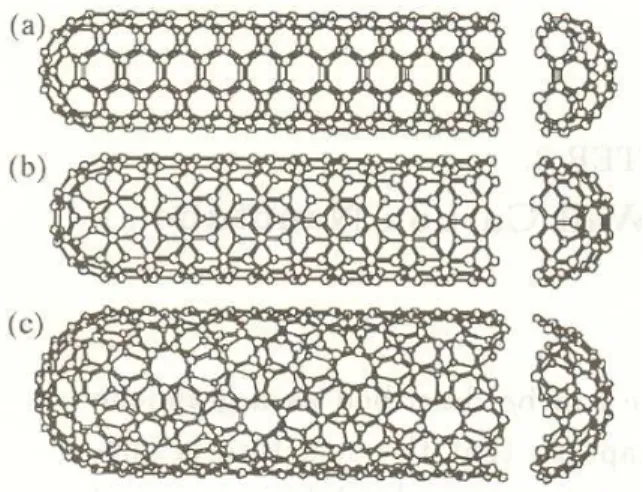
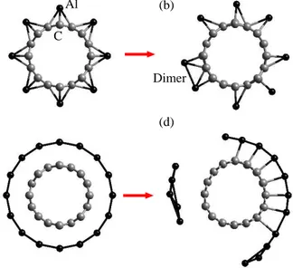
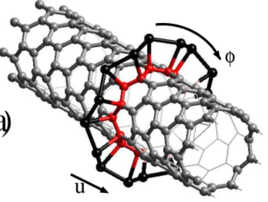
Metal coverage on single-wall carbon nanotubes : metal nanoring and nanotube formation
Tam metin
Şekil


Benzer Belgeler
The proposed automatic video based fire detection algorithm is based on four sub-algorithms: (i) detection of fire colored moving objects, (ii) temporal and (iii) spatial wavelet
Moreover, with the appropriate choice of excess and shortage costs incurred at the end of a single period, it also provides a good myopic approximation for an infi- nite
Keywords: political power, power sources, civil-military relations, Turkish Armed Forces, military intervention, military, army,
We derive transformation, commutation, and uncertainty relations between coordinate multiplication, differentiation, translation, and phase shift operators making
The pro- posed approach applies progressive morphological filtering to compute a normalized DSM from the LiDAR data, uses thresholding of the DSM and spectral data for a
We model the problem as a two stage stochastic mixed integer nonlinear program where the first stage determines the departure time of new flights and the aircraft that is leased..
With [1] and the present paper the algebraic structure of the J -groups of complex projective and lens spaces is completely determined and there is nothing more to do on the
an electrical equivalent circuit will be presented to predict the behavior of the resonator without finite element simulations.. Finally, simulation results will be
