Hilmi Volkan Demir, and Arseniy I. Kuznetsov
*
Cite This:ACS Nano 2020, 14, 7338−7346 Read Online
ACCESS
Metrics & More Article Recommendations*
sı Supporting Information ABSTRACT: On-chip light sources are critical for the realization of fullyintegrated photonic circuitry. So far, semiconductor miniaturized lasers have been mainly limited to sizes on the order of a few microns. Further reduction of sizes is challenging fundamentally due to the associated radiative losses. While using plasmonic metals helps to reduce radiative losses and sizes, they also introduce Ohmic losses hindering real improvements. In this work, we show that, making use of quasibound states in the continuum, or supercavity modes, we circumvent these fundamental issues and realize one of the smallest purely semiconductor nanolasers thus far. Here, the nanolaser structure is based on a single semiconductor nanocylinder that intentionally takes advantage of the
destructive interference between two supported optical modes, namely Fabry−Perot and Mie modes, to obtain a significant enhancement in the quality factor of the cavity. We experimentally demonstrate the concept and obtain optically pumped lasing action using GaAs at cryogenic temperatures. The optimal nanocylinder size is as small as 500 nm in diameter and only 330 nm in height with a lasing wavelength around 825 nm, corresponding to a size-to-wavelength ratio as low as 0.6. KEYWORDS: dielectric nanoantennas, laser, nanolaser, bound state in the continuum, Mie resonance, gallium arsenide
I
n the past decade, resonant dielectric nanoantennas have emerged as a promising platform for nanophotonic applications. Low Ohmic losses and CMOS compatibility, accompanying small form factors, are the key advantages of these systems that make them particularly attractive for industrial applications as compared to prior designs based on plasmonic metals.1In recent years, moreover, significant efforts are being made in combining dielectric nanoantenna concepts with active material platforms2 to extend this promising approach toward efficient directional light sources. By now, the use of dielectric nanoantennas in emission processes has been mainly focused on enhancingfluorescence from molecules,3−8 enhancing the Raman signal9−11 and enhancing photo-luminescence (PL) from the nanoantenna material itself.12−15 Due to the limited quality factors (Q factors) of low-order modes excited in dielectric nanoantennas, lasing has not been demonstrated yet for particle sizes significantly smaller than the wavelength, with the recent exceptions of micrometer-sized systems in which subwavelength nanoantennas are arranged in lattices.16,17 Hence, besides strongly dissipative systems involving metals,2,18on-chip lasers have been mostly restricted to spatially extended systems with sizes on the order of a few microns.The smallest fully dielectric lasers were experimentally demonstrated using suspended disk structures.19,20High-order
Mie-type modes (i.e., whispering gallery modes) were used in those designs to achieve lasing. In this regard, the smallest nanolaser reported consisted of a disk on top of a pedestal with a diameter of 627 nm, operating in the fourth-order Mie resonance and emitting at a wavelength of 870 nm, which corresponds to a size/wavelength ratio ζ = 0.72.20 Very recently, one of the smallest, fully dielectric, single-particle-based laser has been demonstrated using perovskites in a nanocube configuration.21 This design also uses the fourth-order Mie-type mode and has a slightly higher size/wavelength ratio ofζ = 0.79 but operates at room temperature. Further reduction of size (i.e., in disk diameter) is challenging for two different reasons. First, using smaller resonators while keeping the same operating wavelength implies necessarily the use of lower order modes. Those present higher radiative losses, which leads to a drop in the Q factor. Second, smaller particles have larger surface-to-volume ratios, which increases the effect Received: April 1, 2020
Accepted: May 27, 2020 Published: May 27, 2020
Downloaded via BILKENT UNIV on February 12, 2021 at 12:02:46 (UTC).
of surface recombination and roughness, resulting in higher losses that make the gain-loss compensation even more challenging. While the second is more difficult to overcome, without improving the fabrication processes and/or including some surface passivation methods, the first still allows some improvement from the design perspective. Thus, different approaches need to be implemented for improving the quality of the cavities in order to achieve lasing in smaller resonators. A recent promising approach to boost the Q factor of a system is engineering it to support a special type of resonant mode called bound state in the continuum (BIC). BICs are nonradiative states, thus perfectly spatially confined, which nevertheless coexist with the continuum of radiative states (i.e., despite the presence of available radiation channels).22 BICs are a general wave phenomenon, first reported in electronic systems and subsequently extended to photonic ones,22 and are true eigenmodes of the system (in fact, often referred to as embedded eigenstates). Strictly speaking, for any system comprising regular materials with ε ≠ 0, μ ≠ 0, ε ≠ ± ∞, or μ ≠ ± ∞, BICs can only be supported if the system is infinite, and their Q factors are infinite.22Parameters of afinite system, however, can be tuned close to the condition of BICs in the corresponding infinite system.23 The obtained quasi-BICs are often referred to in the literature as supercavity modes and possess finite but high Q factors.23 This makes supercavity modes or quasi-BICs useful for many photonics applications,22,24including, for example, sensing25,26and high-harmonic generation.27−31
Regarding the use of BICs for lasing, one of thefirst quasi-BIC lasers was demonstrated in 1985. It supported a symmetry-protected quasi-BIC by suppressing radiation into the transverse directions in a 1D distributed feedback laser
cavity.32 After that, similar quasi-BIC principles were demonstrated in many photonic crystal surface-emitting laser devices.22In recent years, quasi-BIC-based lasing results have been shown for on-chip systems based on nanoparticle arrays.16,17 Going beyond the BIC supported by spatially extended systems toward single particle configurations, it should be mentioned that a spatially confined system can only support a true BIC if it contains some region in which the permittivity tends to zero.33,34 Nevertheless, several recent reports have theoretically predicted that it should, still, be possible to obtain, if not a true BIC, but a quasi-BIC or a supercavity mode in such a simple system as a single dielectric nanocylinder.28,35,36This quasi-BIC has a Friedrich−Wintgen nature and allows some degree of radiation to escape the system. Thus, by reciprocity, it is also possible to excite it by external sources. Recent experimental studies have, indeed, demonstrated the excitation of these quasi-BICs in a single cylinder at GHz37 and optical30 frequencies. However, no experimental results of lasing in supercavity regime for a single semiconductor nanoparticle have been shown so far. In this work, elaborating on the BIC concept, we report single dielectric nanoparticle laser working in supercavity regime. This also enables the realization of fully dielectric nanolaser operating in the third azimuthal order mode for a particle on a substrate, with size/wavelength ratio as low asζ = 0.6. RESULTS AND DISCUSSION
We designed our cylindrical nanoresonator to support a quasi-BIC that originates from the strong interaction of two resonant modes: a Mie-like mode (which strongly depends on the diameter of the cylinder and is largely insensitive to its height) and a Fabry−Perot (FP)-like mode (which is formed by the
Figure 1. Simulated characteristics of a single GaAs nanocylinder (ε = 13) in vacuum. (A, B) Illustration of the dielectric cylinder in vacuum during scattering simulations (A) andQ factor (near-field, far-field) simulations (B). (C) Scattering efficiency map Qscaas a function of the
dimensionless parametersxH=πH/λ (the size parameter) and ρ = D/H (the cylinder aspect ratio). The alternative x- and y-axis correspond
to the wavelength and diameter obtained when the height of the cylinder isfixed at H = 345 nm. The peak positions and the Q factors of the modes, obtained from theQ factor simulations, are shown by black circles, their area being directly proportional to the value of the Q factor. The results of theQ factor simulations are shown for the quasi-TE modes of azimuthal order i = 3 (labeled TE3and’TE3). Only these two
modes are displayed in order to highlight the anticrossing of the modes TE320and TE312andQ factor evolution as a function of the diameter
and wavelength (theQ factor reaches its maximum value for the optimal parameters indicated by a point β which is the supercavity mode point). The insets show the electric near-field maps in the YZ plane passing through the center of the cylinder for different regimes of the mode TE3. (D, E) Simulated nearfields of the supercavity mode in the XY (D) and YZ (E) planes of the cylinder, respectively. White lines in
(D, E) show the cylinder boundaries. (F) Simulated 3D far-field radiation pattern corresponding to the point β. (G) 2D projection of the simulated far-field radiation pattern corresponding to the point β. The white dashed circle shows the range of wave-vectors collected by a 0.55 NA objective (similar to the one used to collect the emission in the lasing experiment).
minimal scattering, occurs at a different point (the dark mode point).37 These two points match exactly for the case of an ideal BIC.37 Thus, there are three main signatures of the emergence of a supercavity mode of this type: anticrossing between Mie-like and FP-like modes, increase in the Q factor for one of the modes, and decrease in its scattering efficiency in the anticrossing region. The use of a supercavity mode reduces the radiative losses of the system (increasing its Q factor several times with respect to a regular Mie mode of the same order)35enabling gain/loss compensation in nanoparticles of a smaller size.
We focus our attention on obtaining lasing from a supercavity mode of azimuthal order i = 3. In particular, we study a single GaAs cylinder standing on a quartz substrate. Due to the relatively low gain of GaAs at room temperature, which is further reduced by the large surface recombination present in small particles, lasing experiments are performed at the liquid nitrogen temperature (i.e., 77 K) to increase the quantum yield of GaAs (note that no surface passivation or any chemical treatment is applied to the nanostructures). When tuning the temperature from 300 to 77 K, the emission peak of GaAs shifts from 870 to 830 nm.16 Thus, in this work, the geometrical parameters of the cylinder (diameter D and height H) are optimized to achieve high Q factors atλ = 830 nm.
To illustrate the physical mechanism behind the supercavity mode formation in a simple way, let usfirst consider a cylinder with a constant relative permittivity ε = 13 (corresponding, approximately, to GaAs at 830 nm wavelength and 77 K) in vacuum. We perform two types of three-dimensional electro-magnetic simulationsscattering simulations and Q factor calculations (illustrated in parts A and B, respectively, ofFigure 1). For the scattering simulations we study illumination of the cylinder by a transverse electric (TE) wave. The TE wave is defined as the one having incident magnetic field polarized along the axis of the cylinder and the electricfield and incident wave vector perpendicular to it as shown inFigure 1A. In the Q factor simulations, we excite TE modes by a pointlike dipole highlighted inFigure 1B (see theMethodsfor more details). We compute the scattering efficiency and the eigenmodes supported by this cylinder as a function of its geometrical parameters using full wave simulations based on the finite-difference time-domain method (see the Methods for the detailed description). The results are shown in Figure 1C. There, we plot the scattering efficiency as a function of the dimensionless parameters xH=πH/λ (i.e., the size parameter, where the height of the cylinder is used as a characteristic dimension) andρ = D/H (the cylinder aspect ratio). Overlaid with the scattering map, we plot the result of the Q factor simulations: quasi-TE eigenmodes (quasi-normal modes) corresponding to the azimuthal order i = 3 are shown by a set of black circles, their area being directly proportional to the
denote the branches (modes) TE3(higher frequency branch) and’TE3(lower frequency branch) that originate from strong
coupling of the modes TE320 and TE312. Along with avoided spectral crossing, a dramatic increase in the Q factor, leading to a maximum (at the supercavity mode point denoted asβ in
Figure 1C) is observed for the mode TE3near the anticrossing
region, indicating that a supercavity mode has been formed. The reduction of the scattering efficiency at slightly higher diameters, with respect to the supercavity mode point of the mode TE3, is less noticeable due to relatively low permittivity.35 The optimum values of dimensionless param-eters for this third azimuthal order mode are xH∼ 1.30 and ρ
∼ 1.47 (the supercavity mode point). For an operational wavelengthλ = 830 nm, these correspond to a cylinder with height H ∼ 344 nm and diameter D ∼ 504 nm. The corresponding Q factor reaches a maximum value of Q = 970. It should be noted that it has been theoretically shown35that an infinite permittivity is formally equivalent to a spatially infinite system in which an ideal BIC may exist. Practically, this means that the higher the permittivity is, the closer to an ideal BIC the supercavity mode is. This explains why in the case of moderate permittivity of GaAs, the supercavity formation leads to a somehow moderate 5-fold increase in the Q factor. This, nevertheless, turns out to be crucial to reduce the lasing threshold for the third azimuthal order mode, as will be shown in the experiment below.
To complete the characterization of the supercavity mode, the near fields and the far-field radiation pattern in the supercavity regime are depicted inFigures 1D−G. From the near-field maps (Figures 1D,E), the TE312 character of the
mode becomes apparent. On the other hand, the far-field pattern (Figure 1F) shows that, along with the regular in-plane lobes, which are common for pure Mie modes, out-of-plane lobes are present as well. This can be explained by the fact that supercavity mode is a hybrid FP-Mie mode and, thus, it cannot be identified as a pure FP mode or a pure Mie mode. A detailed analysis of the evolution of the near-field distribution around the supercavity regime confirms that the mode TE3has indeed three different regimes, evolving from a Mie-like one
(Figure 1C at pointα) to the Supercavity one (Figure 1C at
pointβ) and finally to a Fabry−Perot-like one (Figure 1C at pointγ). Note that in optical experiments we collect the very edge of the emission side lobes of the supercavity mode, as expected from the simulated radiation pattern inFigure 1G.
To experimentally demonstrate lasing for the analyzed third-order supercavity mode, GaAs nanocylinders standing on a quartz substrate are fabricated using the method reported in ref
16. First, a GaAsfilm grown on top of a commercially available GaAs wafer with a sacrificial layer of AlAs is transferred to a quartz substrate using the technique known as epitaxial lift-off38followed by a direct bonding process developed in-house
using a wafer bonding system. The transferred film is then etched to a desired thickness using inductively coupled plasma (ICP) method. The nanocylinder pattern is then defined using a standard e-beam lithography with hydrogen silsesquioxane (HSQ) as a negative resist. Thefinal structure is formed by an additional dry-etching step (see the Methods for a more detailed information). The SEM image of one of the fabricated nanostructures is shown in the inset ofFigure 2B. Note that, despite their low index, the presence of the quartz substrate and the remaining capping HSQ layer affects the spectral position and the Q factor of the supercavity mode. Thus, we reoptimize the parameters of the cylinder to account for them,
obtaining a maximum Q factor of 280 for optimum values of the dimensionless parameters xH ∼ 1.29 and ρ ∼ 1.47, corresponding to the cylinder height H ∼ 340 nm and diameter D∼ 500 nm at λ = 830 nm (the complete analysis of the modes of the reoptimized geometry will be presented in details later in the text). The height of the GaAs cylinders obtained in the fabricated samples is close to the targeted one, around 330 nm (measured using reflectometer and tilted SEM images). The sample is then cooled down to 77 K using liquid nitrogen for further optical characterization (see the Methods for details).
Figure 2. (A) Normalized photoluminescence spectrum measured from GaAsfilm without HSQ (red) and with 150 nm layer of HSQ on top (black). (B) Normalized experimental dark-field scattering spectrum of a single GaAs nanocylinder with parameters D = 500 nm and H = 330 nm. Inset: exemplary SEM image of the fabricated nanostructure.
Figure 3. Lasing action in a GaAs nanocylinder. (A) Evolution of the emission spectrum of the GaAs nanocylinder with diameterD = 500 and heightH = 330 nm at different pumping fluences. (B) Log−log plot of output emission intensity versus pumping laser fluence showing the transitions from spontaneous emission (SE) to amplified spontaneous emission (ASE) and finally to lasing. (C) Peak position and fwhm of the lasing peak extracted from the emission spectra. (D) Intensity autocorrelation histogram for 50μm × 50 μm GaAs square at the pumping laserfluence F = 764 μJ/cm2 and for the single GaAs nanocylinder of diameter 500 nm and height 330 nm for the pumping
fluences (E) F = 382 μJ/cm2
and known to have non-negligiblefluorescence when treated with e-beam and high temperatures.39,40Indeed, for GaAsfilm with HSQ resist on top, the measured photoluminescence
(Figure 2A) has a broad emission spectrum from 700 to 850
nm (a long passfilter is used to cut the pump at 700 nm), beyond that for GaAs alone which has a relatively narrow PL spectrum from 800 to 850 nm. The above-mentioned broad spectrum is attributed to the photoluminescence of GaAs combined with that of silicon nanocrystals formed in the silica matrix of cured HSQ (whose PL can range from 650 to 800 nm),40which, in our case, most probably arises due to the high energy electron beam exposure, in a chemical reaction analogous to that happening during thermal annealing.41 Thus, in our experiments, the photoluminescence of both Si nanocrystals in cured HSQ42and GaAs itself can provide gain for our nanolasers with different resonance wavelengths.
With this information in mind, we now move to the optical characterization of the nanocylinders at cryogenic temper-atures, first studying their scattering spectra, to identify the formation of the supercavity mode, and then their emission under optical pumping. Figure 2B shows the characteristic dark-field scattering spectrum of a single GaAs nanocylinder with D = 500 nm and H = 330 nm (as measured using SEM). From our theoretical analysis, we expect the cylinder to support the supercavity mode at around 830 nm for these dimensions. Indeed, one can observe the emergence of a very narrow peak in the experimental spectrum at∼828 nm, in very good agreement with what is expected from the simulations, thus confirming the presence of the quasi-BIC mode. To demonstrate lasing action, we optically pump the nano-cylinders using a femtosecond laser (with a wavelength of 530 nm, 200 fs pulse duration and 20 kHz repetition rate) and collect the PL using a microspectrometer setup (see detailed information in the Methods). Nanocylinders have been fabricated with a 20μm spacing, and the pumping laser spot size is ∼5 μm in diameter, ensuring that each cylinder is individually irradiated during optical measurements.Figure 3A shows the PL spectrum evolution of the GaAs nanocylinder with diameter D = 500 nm and height H = 330 nm, supporting the supercavity mode, when pumped under different laser fluences. It can be seen that when the pumping fluence is larger than 260μJ/cm2, a pronounced, narrow peak appears at∼825 nm. By plotting the integrated emission intensity versus the pumpingfluence in log−log scale (Figure 3B) one can clearly see the “S” shape that indicates the transition from spontaneous emission (SE) to amplified spontaneous emission (ASE) andfinally to lasing, with a lasing threshold of ∼300 μJ/ cm2. The PL peak position and full-width-at-half-maximum
(fwhm) as a function of the pumpingfluence, extracted from the spectra, are shown inFigure 3C. Based on the fwhm, we observe a maximum Q factor of 235 in the lasing regime (in
to the relatively bad thermal-dissipation setup (single GaAs nanopillar on quartz) used in our lasing experiment, we believe that thermal broadening effect also contributes to the broadening of the lasing peak. This explains the drop of the Q factor from 500 to 235 as shown inFigure 3C.
To further confirm the coherent nature of the lasing emission, autocorrelation measurements using a Hanbury− Brown−Twiss setup16,45are performed. Parts D−F ofFigure 3
show coincidence counts at different time delays for three different regimes: SE (Figure 3D), ASE (Figure 3E), and lasing
(Figure 3F). The normalized second-order correlation function
at zero time delay g2(0) is defined as the ratio between
coincidence count number of the pulse at zero time delay and an averaged count number over 22 other neighboring pulses. It is noted that the autocorrelation measurement for SE (Figure 3D) is performed on relatively large patterned GaAs squares (of 50 μm × 50 μm). This is to ensure that an adequate amount of signal can be collected and analyzed. It, however, does not change the nature of the SE from the materials composing the nanolaser. Due to their larger size, the photoluminescence intensity of these squares is several times greater than that of the single GaAs nanocylinder used to measure g2(0) in the ASE and lasing regimes, which explains
why the coincidence count number in Figure 3D is substantially higher than those of Figures 3E,F. The g2(0)
for the SE case is calculated to be 1.002, which is significantly smaller than the theoretical value for an ideal thermal light source (i.e., g2(0) = 2). This is because the coherence time of
the SE is much lower than the detection limit of our experimental setup (∼81 ps), in accordance with similar observations reported in earlier studies.16,46 Nevertheless, we are able to measure a clear decrease in g2(0) upon transitioning
between the ASE and lasing regimes, as shown inFigure 3E,F, with the g2(0) reducing from 1.16 (for ASE regime, F = 382
μJ/cm2) to 1.008 (for lasing regime, F = 433 μJ/cm2) and,
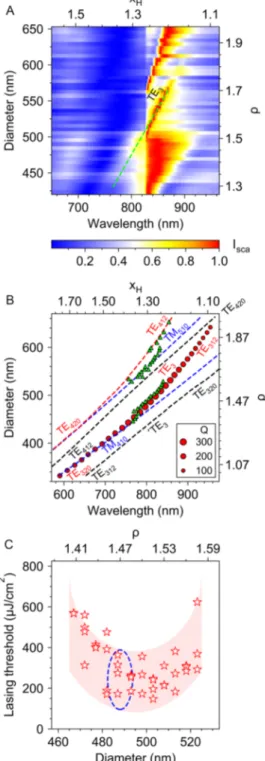
thus, clearly indicating the coherent behavior of the nanolaser. We now prove that lasing is indeed obtained for the third azimuthal order supercavity mode by studying how a slight detuning of the geometrical parameters from the optimal ones affects the performance of the system. For that, lasing and dark-field scattering measurements are carried out for cylinders of the same height, namely H = 330 nm, but with diameters above and below the optimum one. In particular, Figure 4A shows the dark-field scattering spectra of GaAs cylinders with diameter ranging from 420 to 653 nm with an increment of∼5 nm. The mode highlighted by green dashed line inFigure 4A corresponds to the third azimuthal order mode TE3from the
simulation (seeFigure 4B). Higher and lower order modes can also be seen from the scattering data inFigure 4A. For a better visualization of the formation of the supercavity mode, the scattering spectra for several selected radii around the
optimum one are depicted inFigure S2A. It should be noted that, due to the presence of high absorption at wavelengths below the excitonic resonance, it is not possible to observe the full evolution of the scattering peak associated with the formation of the supercavity mode (from broad to narrow and back to broad) but only the narrowing of the resonance. Thus, we explore an alternative experimental method, relying on the analysis of lasing threshold, to prove that the third azimuthal order TE mode used for lasing indeed undergoes the formation of the supercavity regime, as explained below.
Figure 4B shows the theoretically obtained (using Q factor
simulations) peak positions of the quasi-normal eigenmodes in the span of parametersλ and D of our interest. In the case of the mode TE3, the corresponding Q factors are also plotted by
red circles, so that the supercavity regime can be readily identified. Superimposed in the same plot, the green triangles depict the experimental lasing peak positions obtained for various disk diameters. As can be seen, there is a good agreement between the simulated peak positions and the lasing peaks observed in the experiment. The discrepancy between theory and experiment is minimal and lays within the error of diameters determined by SEM and the possible slight deviations in the material parameters. Importantly, we can achieve lasing for the third azimuthal order mode TE3 for a
relatively wide range of cylinder diameters due to the low divergence of quality factor near the optimal value. This gives usflexibility to tune the emission wavelength of the nanolaser within the gain spectrum of the active materials involved (note that, in our case, these refer not only to GaAs, but also to the Si nanocrystals obtained inside HSQ resist after the e-beam exposure). Besides the mode TE3, lasing is also obtained for bigger nanocylinders supporting higher azimuthal order modes (up tofifth-order TM510mode as shown in Figure 4B). It is important to note that, for nanocylinders with diameters close to the optimum (D ∼ 500 nm), the third-order mode of interest (TE3) and the fourth-order Mie mode (TM410) are
spectrally close (∼20 nm away from each other, according to the Q factor simulations, as can be seen inFigure 4B). Thus, it is crucial to observe both the third- and fourth-order modes in the lasing experiments to unequivocally prove that the mode TE3is identified correctly. The detailed view of the emission spectra contributed by both these modes simultaneously is shown inFigure S2B. Moreover, as can be seen inFigure 4B, the lasing peak positions for all modes (third, fourth, and higher azimuthal orders) match well with the theory, further supporting the correct identification of the mode TE3.Figure S3shows additional information on the modes TE3and TM410 obtained from the simulations. The overlap of the near-field
Figure 4. Optical characteristics of the mode TE3in the vicinity of
the supercavity regime. (A) Normalized experimental dark-field scattering spectra of GaAs nanocylinders withfixed height H = 330 nm and varying diameterD = 420−653 nm with an increment of 5 nm. The green dashed line is a guide to eyes indicating the mode TE3. (B) Theoretically obtained peak positions of the modes
supported by a single dielectric nanocylinderε = 13 on a substrate, retrieved from the Q factor simulations, shown in the region of interest of dimensionless parametersxH,ρ. The alternative x- and
y-axis correspond to the wavelength and diameter obtained when the height of the cylinder is fixed at H = 332 nm. The modes denoted as TE320 and TE312 are strongly coupled which is
manifested by the anticrossing. At optimal parameters these modes destructively interfere in the farfield which leads to the formation of the supercavity regime for the mode TE3for which
the correspondingQ factors are indicated by red circles (their area being directly proportional to the value of theQ factor). Strong
Figure4. continued
coupling of the modes TE420 and TE412 manifests itself as an
avoided resonance crossing. Modes TM410and TM510are regular
Mie modes. The green triangles show the experimentally obtained lasing peak positions for cylinders withfixed height H = 330 nm and different diameters. (C) Measured lasing threshold values (depicted as red stars) shown as a function of the diameter of the nanocylinder for the mode TE3. The red shadowed area is a guide
to eyes. The vicinity of the optimal diameter value is highlighted by the blue dashed line (where the mode TE3 undergoes the
supercavity regime in theory, ρ ∼ 1.47). This has a slight discrepancy with experimental results, where the minimal thresh-old is obtained atρ ∼ 1.51.
diameters around the optimum, as shown in Figure 4C. For each diameter, two to four similar nanocylinders are measured to increase the statistic accuracy. As can be seen from the plot
in Figure 4C, the lasing threshold has a minimum in the
vicinity of D = 500 nm, indicating an increase in the Q factor of the mode for this diameter, which is in a good agreement with the theoretically obtained behavior for the supercavity condition.
CONCLUSION
In summary, using the concept of quasi-bound states in the continuum or supercavity modes, we have demonstrated lasing action at cryogenic temperatures in a single GaAs nanocylinder fabricated on a quartz substrate. The nanolaser has a size-to-wavelength ratio as low as 0.6, which, to the best of our knowledge, is one of the lowest values demonstrated for purely semiconductor nanolasers so far. This became possible by engineering two resonances supported by the system, namely, the Mie resonance and the Fabry−Perot resonance, to achieve a quasi-bound state in the continuum, the so-called supercavity mode, via mutual destructive interference of the resonances in the farfield at the targeted lasing wavelength. As compared to previous approaches, the present design does not need the particle to be suspended in air and does not rely on modes of high azimuthal orders, which increases the robustness of the device. We believe that this approach can further be brought to room-temperature operation by using higher gain materials or surface passivation techniques. GaAs is known to have a strong nonradiative recombination due to surface defects which significantly lowers its gain property. There are two ways to reduce the surface recombination: first, using a surface passivation by chemical method (passivating using sulfide compounds such as P2S5, (NH4)2S, Na2S, etc.), and second, using a passivation layer like AlGaAs or multiquantum well (MQW) structure of AlGaAs/GaAs. Such MQW structure, which is widely used in high-efficient LEDs and lasers, is a good candidate for room-temperature operation for this type of laser if we can preserve its emitting property during the dry-etching process. In the future, with the use of electrical pumping and radiation out-coupling strategies, the presented concept can be useful for smaller, Ohmic-loss-free nanolasers, with potential applications in photonic circuits and beyond. METHODS
Numerical Simulations. Numerical simulations were performed using an FDTD commercial software (Lumerical FDTD Solutions). There are two types of numerical simulations carried out in this work: nanoparticle scattering simulations and Q factor calculations. In nanoparticle scattering simulations, the cylinder was irradiated by a plane wave using total-field scattered-field (TFSF) source. This source separates the scatteredfield from the incident field, which allows us to
was placed in the vicinity of the antinode of the electricfield of the desired mode with its dipole moment parallel to the electricfield at that point (as, for example, depicted inFigure 1B, for excitation of quasi-TE modes). Time-dependent electric and magneticfields were recorded using nine pointlike time monitors, randomly placed inside the cylinder. After that, the spectrum was calculated for each monitor using fast Fourier transform (FFT). Then the spectra were averaged over the number of monitors obtaining the spectrum for Q factor calculations. The resonant peaks in the spectrum were fit by a Lorentzian function to obtainΔfi, fwhm for the ith resonance. The Q
factor of the ith resonance was calculated using Q = fi/Δfiwhere fiis
the frequency of the ith resonance. The far-field 3D pattern of the modes was computed using a box monitor completely surrounding the cylinder. The far-field 2D pattern of the modes was obtained using a plane monitor (perpendicular to the z axis) located above the cylinder.
In order to account for the real experimental conditions, additional numerical simulations and optimization were performed considering that the dielectric nanocylinder is placed on a quartz substrate and has a capping HSQ layer on top, as can be seen in the SEM image in the inset ofFigure 2B. In those simulations, we assumed that the cylinder had a constant relative permittivityε = 13, that the HSQ cylinder on top had a height of 150 nm and a constant refractive index nHSQ=
1.41 and that the substrate had a constant refractive index nsubstrate=
1.46.
Sample Nanofabrication. GaAs wafer with an epitaxial structure of i-GaAs (500 nm)/AlAs (100 nm)/undoped⟨100⟩ GaAs (625 nm) was purchased from Semiconductor Wafer, Inc., Taiwan. Epitaxial lift-off38technique was used to transfer the top, high quality GaAsfilm (500 nm) from the wafer to a quartz substrate. In the process, black wax (i.e., Apiezon W) was applied on the top i-GaAs layer and thermally annealed at 90°C for about 30−60 min to realize a slightly domed surface. After that, hydrofluoric acid (HF) solution (∼5 wt % in H2O) was used to etch the sacrificial layer (AlAs) and GaAs
epitaxialfilm was then lifted off. Direct bonding process was used to attach thefilm to the quartz substrate using a wafer bonder system (EVG 510). Inductively coupled plasma reactive ion etching (ICP RIE) tool (Oxford PlasmaLab System 100) was used to etch GaAs film to a desired thickness. Standard electron beam lithography procedure (Elionix ELS-7000 system) was used to fabricate nanocylinders mask using hydrogen silsesquioxane resist (HSQ, Dow Corning XR-1541-006) along with ESpacer (E-spacer 300Z) to improve the conductivity during e-beam exposure. The unexposed resist was removed using 25% tetramethylammonium hydroxide (TMAH) developer. Finally, the patterned GaAs film was etched using ICP RIE. Nanocylinders were fabricated with a 20μm spacing. That period was chosen in such a way that each cylinder would be individually irradiated during subsequent optical measurements, thus acting as an isolated nanoparticle.
Optical Characterization. All optical measurements were performed in a microspectrometer setup which consists of an inverted microscope (Nikon Ti-U) and a spectrometer system (Andor SR303i spectrograph coupled with a 400× 1600-pixel Electron Multiplying Charge-Coupled Device - Newton 971 EMCCD). For lasing and photoluminescence measurements, a Ti:sapphire femtosecond laser (Coherent, MIRA 900) was used. The pumping wavelength was
tuned to∼530 nm by using an optical parametric amplifier (Coherent OPA 9450, RegA). The pulse duration and repetition rate after OPA are∼200 fs and 20 kHz, respectively. The laser beam was focused on the nanocylinder using a 50X dark-field (DF) microscope objective (Nikon, CFI LU Plan DF, numerical aperture NA = 0.55) resulting in a laser spot of ∼5 μm in diameter. The dark-field scattering was measured in a backward scattering configuration using the same microscope objective with white light excitation from a halogen lamp. Transmission of GaAs thinfilm was measured using another halogen lamp excitation. The absorption was calculated by the formula A = 2− log10(%T). All spectrally resolved measurements were carried out with
150 grooves/mm, 800 nm blading grating and the spectrograph slit width of 100 μm resulting in a spectral resolution of ∼1 nm. All measurements were performed at cryogenic temperatures. For that, the sample was placed onto the coldfinger of a cryostat (Janis, ST-500). The chamber was vacuumed to 3× 10⁻³Torr by an oil pump before being cooled to 77 K using liquid nitrogen.
Autocorrelation Measurements. Autocorrelation measure-ments were carried out using a Hanbury−Brown−Twiss setup. The emission signal in our microscopic lasing measurement setup was routed into a multimodefiber (Thorlabs GIF625, 62.5 μm core). The signal was then sent to a 50:50 opticalfiber beamsplitter with each node coupled with a low-jitter avalanche photodiodes (Micro Photon Devices, PDM series with a timing jitter of 35 ps fwhm). Coincident clicks on the two photodiodes were recorded using a time-tagging device (qutools, QuTAU, timing resolution 81 ps).
ASSOCIATED CONTENT
*
sı Supporting InformationThe Supporting Information is available free of charge at
https://pubs.acs.org/doi/10.1021/acsnano.0c02730.
Measured absorption of the GaAsfilm (Figure S1), one-dimensional spectra, obtained in the scattering and lasing experiments (Figure S2), and the Q factor and near-field analysis of the modes TE3and TM410(Figure
S3) (PDF)
AUTHOR INFORMATION Corresponding Author
Arseniy I. Kuznetsov − Institute of Materials Research and Engineering, A*STAR (Agency for Science, Technology and Research), Innovis, Singapore 138634;
orcid.org/0000-0002-7622-8939; Email:
[email protected] Authors
Vasilii Mylnikov − Institute of Materials Research and Engineering, A*STAR (Agency for Science, Technology and Research), Innovis, Singapore 138634; LUMINOUS! Center of Excellence for Semiconductor Lighting and Displays, The Photonics Institute, School of Electrical and Electronic Engineering, School of Physical and Mathematical Sciences, Nanyang Technological University, Singapore 639798 Son Tung Ha − Institute of Materials Research and Engineering,
A*STAR (Agency for Science, Technology and Research), Innovis, Singapore 138634; orcid.org/0000-0002-5475-8365
Zhenying Pan − Institute of Materials Research and Engineering, A*STAR (Agency for Science, Technology and Research), Innovis, Singapore 138634
Vytautas Valuckas − Institute of Materials Research and Engineering, A*STAR (Agency for Science, Technology and Research), Innovis, Singapore 138634
Ramón Paniagua-Domínguez − Institute of Materials Research and Engineering, A*STAR (Agency for Science, Technology and
Research), Innovis, Singapore 138634; orcid.org/0000-0001-7836-681X
Hilmi Volkan Demir − LUMINOUS! Center of Excellence for Semiconductor Lighting and Displays, The Photonics Institute, School of Electrical and Electronic Engineering, School of Physical and Mathematical Sciences, Nanyang Technological University, Singapore 639798; Bilkent University UNAM -Institute of Nanotechnology and Materials Science, Department of Electrical and Electronic Engineering, Department of Physics, Bilkent University, Ankara 06800, Turkey; orcid.org/0000-0003-1793-112X
Complete contact information is available at:
https://pubs.acs.org/10.1021/acsnano.0c02730 Author Contributions
R.P.-D. and A.I.K. conceived the idea. V.M. performed numerical simulations. Z.P. performed epitaxial lift-off of the GaAs film, its bonding to the quartz substrate and etching. V.M. performed etching, electron beam lithography and etching after EBL. V.V. performed SEM measurements. S.T.H. constructed the optical setup, performed all optical measurements and their data processing. All authors discussed the results. V.M. wrote thefirst draft of the manuscript and all authors worked on it. R.P.-D., H.V.D., and A.I.K. coordinated and supervised the work.
Notes
The authors declare no competingfinancial interest. ACKNOWLEDGMENTS
The authors acknowledge Leonid Krivitsky (IMRE, A*STAR) and Victor Leong Xu Heng (IMRE, A*STAR) for processing autocorrelation function measurements data. The authors acknowledge the financial support from A*STAR: SERC Pharos program, Singapore (Grant No. 152 73 00025) and Singapore International Graduate Award.
REFERENCES
(1) Kuznetsov, A. I.; Miroshnichenko, A. E.; Brongersma, M. L.; Kivshar, Y. S.; Luk’yanchuk, B. Optically Resonant Dielectric Nanostructures. Science 2016, 354, aag2472.
(2) Paniagua-Domínguez, R.; Ha, S. T.; Kuznetsov, A. I. Active and Tunable Nanophotonics with Dielectric Nanoantennas. Proc. IEEE 2020, 108, 749−771.
(3) Krasnok, A.; Caldarola, M.; Bonod, N.; Alù, A. Spectroscopy and Biosensing with Optically Resonant Dielectric Nanostructures. Adv. Opt. Mater. 2018, 6, 1701094.
(4) Regmi, R.; Berthelot, J.; Winkler, P. M.; Mivelle, M.; Proust, J.; Bedu, F.; Ozerov, I.; Begou, T.; Lumeau, J.; Rigneault, H.; García-Parajó, M. F.; Bidault, S.; Wenger, J.; Bonod, N. All-Dielectric Silicon Nanogap Antennas to Enhance the Fluorescence of Single Molecules. Nano Lett. 2016, 16, 5143−5151.
(5) Trofymchuk, K.; Reisch, A.; Didier, P.; Fras, F.; Gilliot, P.; Mely, Y.; Klymchenko, A. S. Giant Light-Harvesting Nanoantenna for Single-Molecule Detection in Ambient Light. Nat. Photonics 2017, 11, 657−663.
(6) Caldarola, M.; Albella, P.; Cortés, E.; Rahmani, M.; Roschuk, T.; Grinblat, G.; Oulton, R. F.; Bragas, A. V.; Maier, S. A. Non-Plasmonic Nanoantennas for Surface Enhanced Spectroscopies with Ultra-Low Heat Conversion. Nat. Commun. 2015, 6, 7915.
(7) Staude, I.; Khardikov, V. V.; Fofang, N. T.; Liu, S.; Decker, M.; Neshev, D. N.; Luk, T. S.; Brener, I.; Kivshar, Y. S. Shaping Photoluminescence Spectra with Magnetoelectric Resonances in All-Dielectric Nanoparticles. ACS Photonics 2015, 2, 172−177.
(8) Bouchet, D.; Mivelle, M.; Proust, J.; Gallas, B.; Ozerov, I.; Garcia-Parajo, M. F.; Gulinatti, A.; Rech, I.; De Wilde, Y.; Bonod, N.;
(12) Zalogina, A. S.; Savelev, R. S.; Ushakova, E. V.; Zograf, G. P.; Komissarenko, F. E.; Milichko, V. A.; Makarov, S. V.; Zuev, D. A.; Shadrivov, I. V. Purcell Effect in Active Diamond Nanoantennas. Nanoscale 2018, 10, 8721−8727.
(13) Rutckaia, V.; Heyroth, F.; Novikov, A.; Shaleev, M.; Petrov, M.; Schilling, J. Quantum Dot Emission Driven by Mie Resonances in Silicon Nanostructures. Nano Lett. 2017, 17, 6886−6892.
(14) Tiguntseva, E. Y.; Zograf, G. P.; Komissarenko, F. E.; Zuev, D. A.; Zakhidov, A. A.; Makarov, S. V.; Kivshar, Y. S. Light-Emitting Halide Perovskite Nanoantennas. Nano Lett. 2018, 18, 1185−1190.
(15) Liu, S.; Vaskin, A.; Addamane, S.; Leung, B.; Tsai, M. C.; Yang, Y.; Vabishchevich, P. P.; Keeler, G. A.; Wang, G.; He, X.; Kim, Y.; Hartmann, N. F.; Htoon, H.; Doorn, S. K.; Zilk, M.; Pertsch, T.; Balakrishnan, G.; Sinclair, M. B.; Staude, I.; Brener, I. Light-Emitting Metasurfaces: Simultaneous Control of Spontaneous Emission and Far-Field Radiation. Nano Lett. 2018, 18, 6906−6914.
(16) Ha, S. T.; Fu, Y. H.; Emani, N. K.; Pan, Z.; Bakker, R. M.; Paniagua-Domínguez, R.; Kuznetsov, A. I. Directional Lasing in Resonant Semiconductor Nanoantenna Arrays. Nat. Nanotechnol. 2018, 13, 1042−1047.
(17) Kodigala, A.; Lepetit, T.; Gu, Q.; Bahari, B.; Fainman, Y.; Kanté, B. Lasing Action from Photonic Bound States in Continuum. Nature 2017, 541, 196−199.
(18) Wang, Z.; Meng, X.; Kildishev, A. V.; Boltasseva, A.; Shalaev, V. M. Nanolasers Enabled by Metallic Nanoparticles: From Spasers to Random Lasers. Laser Photonics Rev. 2017, 11, 1700212.
(19) Zhang, Z.; Yang, L.; Liu, V.; Hong, T.; Vahala, K.; Scherer, A. Visible Submicron Microdisk Lasers. Appl. Phys. Lett. 2007, 90, 111119.
(20) Song, Q.; Cao, H.; Ho, S. T.; Solomon, G. S. Near-IR Subwavelength Microdisk Lasers. Appl. Phys. Lett. 2009, 94, 061109. (21) Tiguntseva, E. Y.; Koshelev, K. L.; Furasova, A. D.; Mikhailovskii, V. Y.; Ushakova, E. V.; Baranov, D. G.; Shegai, T. O.; Zakhidov, A. A.; Kivshar, Y. S.; Makarov, S. V. Single-Particle Mie-Resonant All-Dielectric Nanolasers. arXiv 2019, 1905.08646https:// arxiv.org/abs/1905.08646(accessed 2019-05-25).
(22) Hsu, C. W.; Zhen, B.; Stone, A. D.; Joannopoulos, J. D.; Soljačić, M. Bound States in the Continuum. Nat. Rev. Mater. 2016, 1, 16048.
(23) Rybin, M.; Kivshar, Y. Supercavity Lasing. Nature 2017, 541, 164−165.
(24) Koshelev, K.; Favraud, G.; Bogdanov, A.; Kivshar, Y.; Fratalocchi, A. Nonradiating Photonics with Resonant Dielectric Nanostructures. Nanophotonics 2019, 8, 725−745.
(25) Tittl, A.; Leitis, A.; Liu, M.; Yesilkoy, F.; Choi, D.-Y.; Neshev, D. N.; Kivshar, Y. S.; Altug, H. Imaging-Based Molecular Barcoding with Pixelated Dielectric Metasurfaces. Science 2018, 360, 1105−1109. (26) Yesilkoy, F.; Arvelo, E. R.; Jahani, Y.; Liu, M.; Tittl, A.; Cevher, V.; Kivshar, Y.; Altug, H. Ultrasensitive Hyperspectral Imaging and Biodetection Enabled by Dielectric Metasurfaces. Nat. Photonics 2019, 13, 390−396.
(27) Carletti, L.; Koshelev, K.; De Angelis, C.; Kivshar, Y. Giant Nonlinear Response at the Nanoscale Driven by Bound States in the Continuum. Phys. Rev. Lett. 2018, 121, 033903.
(28) Koshelev, K.; Bogdanov, A.; Kivshar, Y. Meta-Optics and Bound States in the Continuum. Sci. Bull. 2019, 64, 836−842.
Second-Order Distributed Feedback Lasers. IEEE J. Quantum Electron. 1985, 21, 151−154.
(33) Silveirinha, M. G. Trapping Light in Open Plasmonic Nanostructures. Phys. Rev. A: At., Mol., Opt. Phys. 2014, 89, 023813. (34) Monticone, F.; Alù, A. Embedded Photonic Eigenvalues in 3D Nanostructures. Phys. Rev. Lett. 2014, 112, 213903.
(35) Rybin, M. V.; Koshelev, K. L.; Sadrieva, Z. F.; Samusev, K. B.; Bogdanov, A. A.; Limonov, M. F.; Kivshar, Y. S. High-Q Supercavity Modes in Subwavelength Dielectric Resonators. Phys. Rev. Lett. 2017, 119, 243901.
(36) Chen, W.; Chen, Y.; Liu, W. Multipolar Conversion Induced Subwavelength High-Q Kerker Supermodes with Unidirectional Radiations. Laser Photonics Rev. 2019, 13, 1900067.
(37) Bogdanov, A. A.; Koshelev, K. L.; Kapitanova, P. V.; Rybin, M. V.; Gladyshev, S. A.; Sadrieva, Z. F.; Samusev, K. B.; Kivshar, Y. S.; Limonov, M. F. Bound States in the Continuum and Fano Resonances in the Strong Mode Coupling Regime. Adv. Photon. 2019, 1, 016001.
(38) Yablonovitch, E.; Gmitter, T.; Harbison, J. P.; Bhat, R. Extreme Selectivity in the Lift-Off of Epitaxial GaAs Films. Appl. Phys. Lett. 1987, 51, 2222−2224.
(39) Hessel, C. M.; Henderson, E. J.; Veinot, J. G. C. Hydrogen Silsesquioxane: A Molecular Precursor for Nanocrystalline Si−SiO2
Composites and Freestanding Hydride-Surface-Terminated Silicon Nanoparticles. Chem. Mater. 2006, 18, 6139−6146.
(40) Zhou, W.-J.; Zheng, Y.-X.; Zhang, C.; Ma, X.-F.; Li, D.-H.; Ma, L.; Hu, F.; Yang, S.-D.; Yang, L.; Gao, M.-Y.; Lu, M.; Zhang, R.-J.; Wang, S.-Y.; Chen, L.-Y. Optical Properties of High Photo-luminescence Silicon Nanocrystals Embedded in SiO2 Matrices
Obtained By Annealing Hydrogen Silsesquioxane. Opt. Mater. 2018, 84, 874−878.
(41) Choi, S.; Word, M. J.; Kumar, V.; Adesida, I. Comparative Study of Thermally Cured and Electron-Beam-Exposed Hydrogen Silsesquioxane Resists. J. Vac. Sci. Technol., B: Microelectron. Nanometer Struct.−Process., Meas., Phenom. 2008, 26, 1654−1659.
(42) Wang, D.-C.; Zhang, C.; Zeng, P.; Zhou, W.-J.; Ma, L.; Wang, H.-T.; Zhou, Z.-Q.; Hu, F.; Zhang, S.-Y.; Lu, M.; Wu, X. An All-Silicon Laser Based on All-Silicon Nanocrystals with High Optical Gains. Sci. Bull. 2018, 63, 75−77.
(43) Numai, T. Fundamentals of Semiconductor Lasers; Springer: Tokyo, 2015.
(44) Saxena, D.; Mokkapati, S.; Parkinson, P.; Jiang, N.; Gao, Q.; Tan, H. H.; Jagadish, C. Optically Pumped Room-Temperature GaAs Nanowire Lasers. Nat. Photonics 2013, 7, 963−968.
(45) Chow, W. W.; Jahnke, F.; Gies, C. Emission Properties of Nanolasers during the Transition to Lasing. Light Sci. Appl. 2014, 3, No. e201.
(46) Pan, S. H.; Gu, Q.; Amili, A. E.; Vallini, F.; Fainman, Y. Dynamic Hysteresis in a Coherent High-β Nanolaser. Optica 2016, 3, 1260−1265.
(47) Bohren, C. F.; Huffman, D. R. Absorption and Scattering of Light by Small Particles; John Wiley & Sons Inc: New York, 1983.