HIGH CAPACITY ANODE MATERIALS FOR
LITHIUM - ION BATTERIES
a thesis submitted to
the graduate school of engineering and science
of bilkent university
in partial fulfillment of the requirements for
the degree of
master of science
in
materials science and nanotechnology
By
¨
Omer Ula¸s Kudu
January, 2017
HIGH CAPACITY ANODE MATERIALS FOR LITHIUM - ION BATTERIES
By ¨Omer Ula¸s Kudu January, 2017
We certify that we have read this thesis and that in our opinion it is fully adequate, in scope and in quality, as a thesis for the degree of Master of Science.
Eda Yılmaz(Advisor)
¨
Omer Da˘g
Mehmet Kadri Aydınol
ABSTRACT
HIGH CAPACITY ANODE MATERIALS FOR
LITHIUM - ION BATTERIES
¨
Omer Ula¸s Kudu
M.S. in Materials Science and Nanotechnology Advisor: Eda Yılmaz
January, 2017
Huge energy demand in the world has caused depletion in non - renewable energy sources, and global climate change due to the consumed fuel exhausts. Renewable energy sources are eco - friendly alternatives. Electrochemical energy storage systems (EESS) are useful tools to store the energy, which is harvested from the renewable sources. Lithium - ion batteries are currently the most pop-ular EESS owing to their several advantages over other systems. However, for their use in high energy demanding applications like electric vehicles, new elec-trode materials with higher capacities are required. Here, we demonstrate two anode materials with high capacities, aluminum and silicon. We address prob-lems regarding their commercial applications and offer solutions. To improve the properties of aluminum, we fabricate aluminum - copper thin films via sputtering, then we apply age hardening to the alloy. We observe that age hardening indeed increase stability of aluminum anodes. In the second work, we synthesize silicon nanoparticles via laser ablation, whose sizes are smaller than 20 nm, and embed them into carbon nanofibers (CNFs) via electrospinning. The electrochemical battery tests are conducted with only CNFs, CNFs with commercial Si nanopar-ticles and CNFs with laser ablased Si nanoparnanopar-ticles. The cyclic stability of these composites are observed along with their rate capabilities.
¨
OZET
L˙ITYUM ˙IYON P˙ILLER˙I ˙IC
¸ ˙IN Y ¨
UKSEK KAPAS˙ITEL˙I
ANOT MALZEMELER˙I
¨
Omer Ula¸s Kudu
Malzeme Bilimi ve Nanoteknoloji, Y¨uksek Lisans Tez Danı¸smanı: Eda Yılmaz
Ocak 2017
D¨unyada y¨ukselen enerji ihtiyacı, yenilenemez enerji rezervlerinin azalmasına, harcanan fosil yakıtların da k¨uresel iklim de˘gi¸simine yol a¸cmasına sebep olmak-tadır. Yenilenebilir enerji kaynaklarından elde edilen enerjiyi saklayabilien elek-trokimyasal enerji depolama sistemleri (EESS), fosil yakıtlara ¸cevre dostu bir al-ternatif olu¸sturmaktadır. Di˘ger sistemlere g¨ore ¸ce¸sitli y¨onlerden avantaj sa˘glayan lityum iyon pilleri, an itibariyle en pop¨uler EESSdir. Fakat, elektrikli ara¸clar gibi y˘gksek enerji t¨uketen uygulamalarda kullanılabilmeleri i¸cin, daha y¨uksek kapa-siteli elektrot malzemeleri gerekmektedir. Bu ¸calı¸smada, aluminyum ve silikon gibi iki farklı y¨uksek kapasiteli anot malzemesini sunulmaktadır. Ticari kul-lanımlarına engel olan problemler i¸saret edilip, ¸c¨oz¨um ¨onerileri sunulmaktadır. Aluminyumun ¨ozelliklerini geli¸stirmek i¸cin, sputtering metodu ile aluminyum bakır ince filmleri ¨uretilip, daha sonra ya¸slandırarak sertle¸stirme metodunu uygu-lanmaktadır. Ya¸slandırarak sertle¸stirme metodunun ger¸cekten de aluminyum anot malzemesinin stabilitesini arttırdı˘gı g¨ozlemlenmi¸stir. Di˘ger ¸calı¸smada ise, lazer ile a¸sındırma y¸sntemini kullanarak, 20 nmden k¨u¸c¨uk silikon nanopar¸cacıklar ¨
uretilip, elektro lif ¸cekimi y¨ontemiyle hazırlanmı¸s karbon nanoliflerin (KNL) i¸cine g¨om¨ulm¨u¸st¨ur. Elektrokimyasal pil testleri; yalnız KNL ile, ticari silikon & KNL kompoziti ile, ve lazer ile a¸sındırma y¨ontemi ile ¨uretilmi¸s silikon & KNL kom-poziti ile ger¸cekle¸stirilmi¸stir. Bu kompozitlerin kapasite stabiliteleri ve de˘gi¸sik akımlardaki performansları g¨ozlenmi¸stir.
Anahtar s¨ozc¨ukler : Lityum iyon pilleri, anot malzemeleri, y¨uksek kapasite, y¨uksek enerji yo˘gunlu˘gu, elektro lif ¸cekimi, ya¸slandırarak sertle¸stirme, silikon,
Acknowledgement
To complete my thesis work here in UNAM, I received great help from many people here, and outside of work. Firstly, I would like to thank Dr. Cevriye Koz for her help in silicon nanoparticle synthesis, and carbon nanofiber fabrication. For their help in laser ablation, I thank T¨urkan Gamze Ulusoy Ghobadi and Amir Ghobadi. I’m grateful to Sa˘gnak Sa˘gkal for handling the sputtering process in aluminum project, and to Seda Kızır for her help in GIXRD measurements. I ap-preciate help of Mustafa G¨uler in TEM measurements. Furthermore, I thank Dr. Eda Yılmaz for her contributions to my education in the field of electrochemistry.
For their moral support, I thank my family, which consists of a fair amount of Kudu’s: Y¨uksel, S¸ennur, Efnan Berk, Fatma G¨ulsima and Yi˘git Eymen. The list continues as follows: My beloved Ayg¨ul Zengin, and electrochemical energy storage laboratory (EESL) members: Mehmetcan Ya˘gcı, Faruk Okur, Kıvan¸c C¸ oban, Mohammad Fathi Tovini and Dr. Bhushan Patil. Last but not least, I’d like to thank my friends Mustafa Fadlelmula, Hatice K¨ubra Kara and Zeynep Orhan for the times we spend during the nights, working in UNAM.
I also want to thank the Scientific and Technological Research Council of Turkey (TUBITAK) for funding our work and laboratory with grant number 214M437.
Contents
1 Introduction 1
1.1 Electrochemical Energy Systems . . . 1
1.2 Working Mechanism of LIBs . . . 2
1.3 Pathway to High Performance Anode Materials . . . 6
1.4 Anode Materials According to Their Chemistry . . . 8
1.4.1 Insertion Based Anode Materials . . . 8
1.4.2 Alloying Based Anode Materials . . . 9
1.4.3 Conversion Reaction Based Anode Materials . . . 9
1.5 Motivation . . . 10
2 Materials & Methods 11 2.1 Materials . . . 11
CONTENTS vii
2.2.2 Electrospinning of Silicon & Carbon Nanofiber Composite 13
2.2.3 Heat Treatment Steps of Silicon & Carbon Nanofiber
Com-posite . . . 16
2.2.4 HF treatment of SC5 . . . 16
2.2.5 Thin Film Deposition of Aluminum and Aluminum - Copper 17 2.2.6 Heat Treatment Steps of Aluminum and Aluminum - Copper 17 2.2.7 Characterization . . . 18
2.2.8 Lithium - Ion Battery Preparation . . . 19
2.2.9 Electrochemical Characterization . . . 20
3 Silicon Based Anode Materials for Li - ion Batteries 22 3.1 Silicon as an Anode Material for Lithium - Ion Batteries . . . 22
3.2 Electrospinning . . . 25
3.3 Silicon & Carbon Nanofiber Composite . . . 26
3.4 Results & Discussion . . . 28
4 Aluminum Based Anode Materials for Li - ion Batteries 49 4.1 Aluminum as an Anode Material for Lithium - Ion Batteries . . . 49
4.2 Age Hardening in Aluminum - Copper Alloys . . . 50
4.3 Age Hardened Aluminum - Copper Thin Film Alloy . . . 52
CONTENTS viii
5 Summary and Future Outlook 73
List of Figures
1.1 Schematic representation of the working mechanism of commercial LIBs . . . 3
1.2 Schematic representation of energy levels of components in LIBs . 4
2.1 a) Photographic image of the silicon nanoparticles which were syn-thesized by laser ablation . . . 12
2.2 Photographic image of the silicon nanoparticle & PAN solutions with a) Silicon nanoparticles as synthesized, b) SiNPA1 and c) SiNPA2 . . . 13
2.3 Photographic image of bead formation in inhomogeneous electro-spun fibers after carbonization, which contains 6 % PAN in its electrospinning precursor . . . 14
2.4 Schematic representation of homogeneous electrospinning silicon nanoparticles & carbon nanofiber composite . . . 14
2.5 Photographic image of the electrospun fibers . . . 15
LIST OF FIGURES x
2.7 Photographic image of (from left to right) SS, aluminum thin film after deposition, aluminum - copper thin film after deposition, alu-minum - copper alloy after age hardening . . . 18
2.8 a) Photographic image of the Swagelok battery cell b) Schematic representation of the components in the battery assembly . . . 19
2.9 Photographic image of a) Biologic Instruments SP - 150 potentio-stat, and b) Landt CT2001A multichannel potentiostat/galvanostat 21
3.1 a) Regional XPS scan for Si 2p of, b) Raman spectra of, c) TEM image of silicon nanoparticles, which are synthesized via laser ab-lation . . . 28
3.2 Regional XPS scans for a) C 1s, b) O 1s, c) N 1s of SC1 before carbonization (black), and after carbonization (red) . . . 28
3.3 SEM images of SC1 a) Before carbonization, b) After carboniza-tion, c) Raman spectrum and d) TG curve of SC1 . . . 30
3.4 Regional XPS scan of SC2 for a) Si 2p and b) C 1s, after carbonization 31
3.5 SEM images of SC2 a) Before carbonization, b) After carboniza-tion, c) Raman spectrum and d) TG curve of SC2 . . . 32
3.6 Regional XPS scans of SC3 (black), SC4 (red) and SC5 (blue) for a) Si 2p and b) C 1s . . . 33
3.7 SEM images (after carbonization) of a) SC3, b) SC4, and c) SC5 . 33
3.8 TG curves (after carbonization) of a) SC3, b) SC4 . . . 34
LIST OF FIGURES xi
3.10 Regional XPS scans of SC5 before (black), and after (red) TGA for a) Si 2p, and b) C 1s . . . 36
3.11 Raman spectrum of SC5 after carbonization . . . 36
3.12 Cyclic voltammograms of a) SC1, b) SC2, and c)SC5, where the first, the second and the third cycles were indicated with black, red, and blue, respectively . . . 37
3.13 Galvanostatic charge/discharge curves of a) First 10 cycles at 100 mA/gcathode, b) Last 10 cycles at 100 mA/gcathode, c) Cyclic
stabil-ity measurement at 20 mA/gcathode between 40th and 90th cycles,
and d) Rate capability measurement between 10th and 40th cycles, of SC1 . . . 38
3.14 Galvanostatic charge/discharge curves of a) First 10 cycles at 100 mA/gcathode, b) Last 10 cycles at 100 mA/gcathode, c) Cyclic
stabil-ity measurement at 20 mA/gcathode between 40th and 90th cycles,
and d) Rate capability measurement between 10th and 40th cycles, of SC2 . . . 40
3.15 Galvanostatic charge/discharge curves of a) First 10 cycles at 100 mA/gcathode, b) Last 10 cycles at 100 mA/gcathode, c) Cyclic
stabil-ity measurement at 20 mA/gcathode between 40th and 90th cycles,
and d) Rate capability measurement between 10th and 40th cycles, of SC3 . . . 41
3.16 Galvanostatic charge/discharge curves of a) First 10 cycles at 100 mA/gcathode, b) Last 10 cycles at 100 mA/gcathode, c) Cyclic
stabil-ity measurement at 20 mA/gcathode between 40th and 90th cycles,
and d) Rate capability measurement between 10th and 40th cycles, of SC4 . . . 42
LIST OF FIGURES xii
3.17 Galvanostatic charge/discharge curves of a) First 10 cycles at 100 mA/gcathode, b) Last 10 cycles at 100 mA/gcathode, c) Cyclic
stabil-ity measurement at 20 mA/gcathode between 40th and 90th cycles,
and d) Rate capability measurement between 10th and 40th cycles, of SC5 . . . 44
3.18 Galvanostatic charge/discharge curves of a) First 10 cycles at 100 mA/gcathode, b) Last 10 cycles at 100 mA/gcathode, c) Cyclic
stabil-ity measurement at 20 mA/gcathode between 40th and 90th cycles,
and d) Rate capability measurement between 10th and 40th cycles, of HF treated SC5 . . . 45
3.19 Galvanostatic charge/discharge curves of HF treated SC5 at 400 mA/gsilicon . . . 46
3.20 SEM images (after cycling) of a) SC1, b) SC2, and c) SC5 . . . . 47
3.21 Nyquist plots of SC1 (black), SC2 (red), SC5 (blue), and HF treated SC5 (green) before cycling . . . 48
4.1 SEM images of a) Uncoated SS, b) Aluminum coated on SS (as coated), c) Aluminum - copper coated on SS (as coated), d) Alu-minum - copper coated on SS (after solutionizing and aging) . . . 53
4.2 SEM image of aluminum - copper coated on SS (after solutionizing and aging) with a higher magnification . . . 54
4.3 EDS elemental mapping of aluminum - copper samples coated on SS before heat treatment . . . 55
4.4 EDS elemental mapping of aluminum - copper samples coated on SS after heat treatment . . . 56
LIST OF FIGURES xiii
4.6 EDS elemental ratios and EDS elemental mapping of aluminum -copper sample coated on SS after heat treatment . . . 58
4.7 XRD patterns of SS substrate (black), aluminum thin film as de-posited (red), aluminum - copper thin film sample as dede-posited (blue), aluminum - copper thin film sample after age hardening (green) . . . 60
4.8 Regional XPS scans for Al 2p, Cu 2p and Fe 2p of SS substrate (black), aluminum thin film as deposited (red), aluminum - copper thin film sample as deposited (blue), aluminum - copper thin film sample after age hardening (green) . . . 61
4.9 SEM image of aluminum after the heat treatment . . . 62
4.10 EDS elemental ratios and EDS elemental mapping of aluminum after the heat treatment . . . 63
4.11 Regional XPS scans for a) Al 2p, b) Cu 2p, c) Fe 2p, and d) XRD spectra of aged hardened aluminum - copper (black) and aluminum after the heat treatment (red) . . . 64
4.12 Cyclic voltammograms of a) Aluminum, b) Age hardened alu-minum - copper alloy and c) The heat treated alualu-minum (1.cycle is black, 2.cycle is red and 3.cycle is blue) . . . 65
4.13 Galvanostatic charge/discharge curves of aluminum thin film in a) the first 10 cycles at 100 mA/g current rate (1.cycle is black, 10.cy-cle is red), b) Cyclic stability measurement at 200 mA/g current rate and c) Rate capability data at different current rates . . . 67
LIST OF FIGURES xiv
4.14 Galvanostatic charge/discharge curves of age hardened aluminum - copper alloy in a) the first 10 cycles at 100 mA/g current rate (1.cycle is black, 10.cycle is red), b) Cyclic stability measurement at 200 mA/g current rate and c) Rate capability data at different current rates . . . 68
4.15 Galvanostatic charge/discharge curves of the heat treated alu-minum in a) the first 10 cycles at 100 mA/g current rate (1.cycle is black, 10.cycle is red), b) Cyclic stability measurement at 200 mA/g current rate and c) Rate capability data at different current rates . . . 70
4.16 SEM image after cycling of a) Aluminum thin film, b) Age hardened aluminum copper alloy and c) Age hardhardened aluminum -copper alloy at a higher magnification . . . 71
4.17 Regional XPS scans for a) Al 2p, b) Cu 2p, c) C 1s, and d) Li 1s of age hardened aluminum - copper alloy before (black) and after (red) cycling . . . 72
A.1 a) High Resolution TEM image of, b) EDX results of the silicon nanoparticles synthesized via laser ablation . . . 88
A.2 Regional XPS scans of SC5 before (black), and after (red) HF treatment for a) Si 2p, b) C 1s, and c) F 1s . . . 89
A.3 a) SEM image of, b) EDS results of SC5 after HF treatment . . . 89
A.4 CV curve of HF treated SC5 . . . 89
A.5 Galvanostatic charge/discharge curves of a) First 10 cycles at 100 mA/gcathode, b) Last 10 cycles at 100 mA/gcathode, c) Cyclic
stabil-ity measurement at 20 mA/gcathode between 40th and 90th cycles,
List of Tables
1.1 Properties of some of the high capacity anode materials for LIBs . 6
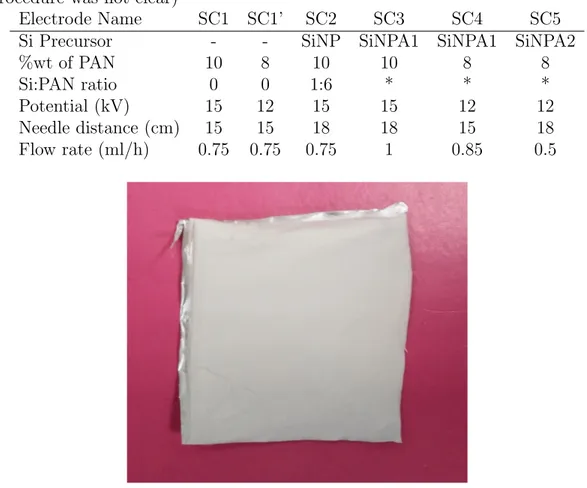
2.1 Parameters and proportions used in electrospinning precursor preparation and electrospinning (The ”*” values are unknown since yield of the synthesis procedure was not clear) . . . 15
Chapter 1
Introduction
1.1
Electrochemical Energy Systems
Expectations from electrochemical energy systems like fuel cells, supercapacitors and batteries have raised further due to quick depletion of fossil fuels, and the pollution and global climate change which are caused by combustion reaction of variety of engines powered by them, in the past few decades [1–3]. Particularly, there has been a boost of attraction to batteries, which have high energy and power density, owing to their use in portable consumer electronic devices such as cellular phones, laptop computers, digital cameras and implantable medical ap-plications. In fact, their worldwide market value was pronounced by ten billion dollars per annum in 2008. However, current performances of commercial batter-ies are still not sufficient for their proper utilization in advanced applications such as future electric vehicles. Batteries, which are to be used in electric vehicles, are expected to provide quick charging, high energy and power density for long travel distances. The search for advanced batteries is particularly focused on lithium -ion batteries (LIBs) since they were made commercially available by Sony in early 1990s, owing to their superiority in terms of power density (5-6 times higher) and energy density (2-3 times higher) compared to other rechargeable battery systems
Although some different electrochemical energy systems like supercapacitors and lithium - air batteries are more advantageous in terms of power density and energy density, respectively, they have their own drawbacks. To illustrate, supercapaci-tors offer poor energy density while lithium - air batteries suffer from poor cycle life, hence LIBs still remain more popular. [7–11]
The essence of predominance of LIBs is associated to the employment of non-aqueous electrolytes because they allow the battery to perform in harsh conditions such as high cell potentials (∼ 4 V), and high operating temperatures. Along with relatively higher energy density, LIBs offer long cycle life and low self - discharge. Furthermore, there is no limitation on partial charging since so - called ”memory effect” does not exist in LIBs. [1,2,4–6] On the other hand, although they possess many advantages over other rechargeable battery systems, commercial LIBs of today could offer only 163 km travelling distance if they are used as energy storage devices in electric vehicles. [12] The standard for an electrochemical energy storage device to be conveniently used in an electric vehicle has been issued by The United States Advanced Battery Consortium (USABC), which claims that the device should provide more than 200 Wh/kg and 300 Wh/L energy density at a discharge rate of C/3 (C indicates the discharge rate at which the device is completely charged/discharged in 1 hour), and at least 80% of its initial capacity should be retained after 1000 cycles. [13, 14] Therefore, there is still much room for improvement in the performance of LIBs.
1.2
Working Mechanism of LIBs
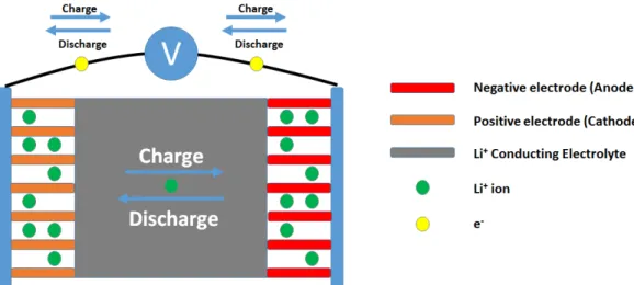
Typically, commercial LIBs are primarily composed of a reductant negative trode (anode), an oxidant positive electrode (cathode), and a non-aqueous elec-trolyte. In operation of the battery, Li+ (Li+) shuttle between the electrodes
(where the name ”rocking - chair cells” comes from). During discharge, Li+ leave
the anode, travels through the electrolyte and intercalate into the cathode. The movement of Li+ are reversed in charging process while the electrons are
trans-acquired/required from/for the ion motion is harvested/stored electrochemically in the battery (see Figure 1.1).
Figure 1.1: Schematic representation of the working mechanism of commercial LIBs
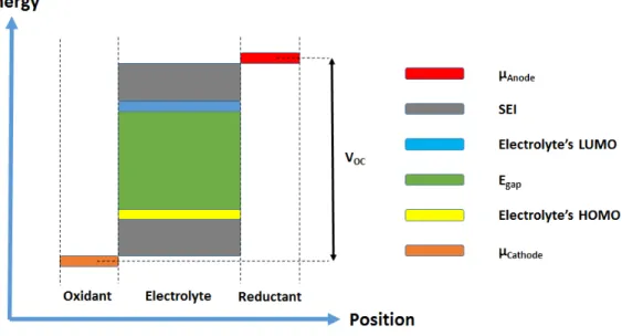
The chemistry happening in LIBs is elaborated in Figure 1.2 further. Open circuit potential of a battery is defined by potential difference between electro-chemical potentials of µAnode and µCathode (anode’s and cathode’s Fermi
ener-gies). On the other hand, energy levels, which correspond to lowest unoccupied molecular orbital (LUMO) and highest occupied molecular orbital (HOMO) of electrolyte, determines the working potential window of the electrolyte [17]. If an anode material of a battery has a higher electrochemical potential than LUMO of the battery’s electrolyte, the electrolyte is reduced by the anode and a pas-sivization layer, also known as solid - electrolyte interface (SEI), will be formed. Similarly, if a cathode material, which has lower electrochemical potential than HOMO of the electrolyte, is hired in a battery, the electrolyte will be oxidized. Since SEI leads to undesired effects such as blocking the electron transfer during battery operation, designing electrode materials, whose electrochemical poten-tials are positioned in range of working potential window of the electrolyte, is crucial [18, 19].
In today’s commercial LIBs, LiCoO2 is the most widely used cathode material
Figure 1.2: Schematic representation of energy levels of components in LIBs
Cathodic reaction:
LiCoO2 ⇐⇒ Li1−xCoO2+ xLi++ xe− (1.1)
Anodic reaction:
xC6+ xLi++ xe− ⇐⇒ xLiC6 (1.2)
Overall reaction:
LiCoO2+ xC6 ⇐⇒ Li1−xCoO2+ xLiC6 (1.3)
Before LIBs’ commercialization, lithium metal was used as anode in lithium batteries, which caused several problems. When lithium is employed in the anode side, parasitic reactions are observed during the operation due to the chemical reaction between lithium and non - aqueous electrolyte. As a result, SEI forms on lithium electrode and prevents further corrosion of the electrode; however, Li+ forms dendrites on the layer that cause short circuit [1]. The dendrite region
is then faced local overheating, which cause serious safety issues [20, 21]. To overcome these issues, lithium insertion compounds have been used as lithium
-anode material that can provide better safety, but it comes with several drawbacks such as low capacity (372 mAh/g), low Li+ ion diffusion coefficient, high volume
change (∼ 9%) during operation and low operating potential (<0.2 V vs Li/Li+
electrode) [22, 23].
There are different lithium transition metal oxides which are conventionally employed as cathode materials (LiMOx, where M is a transition metal) for LIBs
[6]. The problem related to transition metal oxides is that they release oxygen from their lattice at high temperatures [24]. Materials having polyanion groups offer relatively higher stability at elevated temperatures [6, 25, 26]. However, although they propose improved safety, they generally suffer from low ionic and electric conductivity, which lead to poor energy and power density [27,28]. There are some ways to overcome conductivity related problems in electrode materials and the methods will be discussed thoroughly in the upcoming sections.
Electrolytes for LIBs are classified according to their physical state at room temperature, which are referred to as solid, liquid and gel electrolytes. Each type is useful for different applications. Liquid electrolytes are generally pre-ferred in portable electronic devices owing to their superior ionic conductivity [29], which leads to better performance at high power applications. Even though solid electrolytes possess poor ionic conductivity at room temperature, they greatly enhance the battery stability and safety. In addition to hindering SEI layer formation in the electrodes, they do not suffer problems related to electrolyte leakage [30]. Gel electrolytes, on the other hand, are introduced to combine the advantages of solid and liquid electrolytes to form an electrolyte with high ionic conductivity, flexibility and safety [31].
1.3
Pathway to High Performance Anode
Ma-terials
Having mentioned the current challenges in lithium - ion battery field, it is clear that anode materials need progression along with the other components. Since this thesis is dedicated to anode materials, they will be the primary focus from this part on. One needs to be careful about some key parameters such as material selection, and the material’s structural formation before offering a new anode material to the field. Hence, these parameters will be elaborated in this section.
Table 1.1: Properties of some of the high capacity anode materials for LIBs
Materials Li C Si Sn Sb Al Mg
Density (g/cm3) 0.53 2.25 2.3 7.3 6.7 2.7 1.3
Lithiated Phase Li LiC6 Li4.4Si Li4.4Sn Li3Sb LiAl Li3Mg
Theor. Cap. (mAh/g) 3862 372 4200 994 660 993 3350 Volume Change (%) 100 9 420 260 200 96 100 Potential vs Li/Li+ (V) 0 0.05 0.4 0.6 0.9 0.3 0.1 Depending on the material to be used as anode; lithium - ion storage capacity of material, energy density of battery and stability of electrode change [32]. The capacity of an electrode is determined by recording the electrochemical reaction’s current and the reaction time during its Li+ ion uptake. Optionally, gravimetric
and volumetric capacities of the electrode could be obtained by taking its weight and volume into account, respectively. Furthermore, energy density of a material is obtained by multiplying the capacity with the potential difference between the anode and the cathode. Thus, a good anode material should offer both high capacity and low electrochemical potential. Some of the possible elements to be used as high capacity anode materials for LIBs, and their properties are listed in Table 1.1 [33]. Nevertheless, materials with electrochemical potentials, which are not in the working potential window of the electrolyte, are susceptible to side reactions, which cause instability in SEI. There are different solutions to this problem such as coating electrode material, or forming various structures
to embed the material into some protective environment, which should have no hindering effect on the cell operation mechanism.
Secondly, ionic and electronic conductivities of electrode material are crucial limiting factors because any hindering effect on electronic and/or ionic movement causes overpotential, and reduces reversibility and energy density. Nevertheless, long intercalation distance of Li+ ion and low electronic conduction could be
fixed by applying some strategies such as forming nano morphologies, doping and/or coating the active material with various type of materials. Particularly, implementing nanochemistry enhances electric conductivity while reducing the diffusion distance for Li+ ions. Consequently the battery life and its energy density is improved [34, 35].
Furthermore, volume changes during cell operation could result in pulveriza-tion of the electrode, which is often observed in high capacity materials. As a result, active material falls off from current collector and does not contribute to electrochemical reaction, which results in large irreversible capacity losses [36]. Pulverization could be prevented by employing strategies that are similar to the ones, which are hired in occasions where stability and conductivity problems are present.
Although size reduction and coating offer a promising pathway for reversible anode materials with high energy density, one should be careful with its design parameters [37–39]. For example, decreasing the active materials’ size leads to higher surface area. Provided that the uncoated surfaces of electrode materials are prone to side reactions and SEI formation, poorly modified nano structure could easily produce large irreversible Li+ ion consumption, increase in the electrode resistance due to electrically insulating SEI layer, and poor Coulombic efficiency [40–42]. At this point, coating the surface of active material can improve the electrode’s reversibility, however, it would form a dead weight in the anode which does not contribute to the redox reaction, hence the gravimetric energy density is compromised [22]. In addition, particle size of an anode material is inversely proportional to its volumetric energy density [43]. Hence, it is critical to optimize
1.4
Anode Materials According to Their
Chem-istry
As mentioned previously, working principle of lithium - ion materials is primarily based on intercalation of Li+ ions to host electrode materials. Moreover, the
im-portance of morphology is emphasized and optimization of structure parameters is suggested in the former sections. According to lithiation mechanism, anode materials are classified as insertion based anode materials, alloying based anode materials and conversion reaction based anode materials. Each mechanism comes with a set of advantage and its limitation, which will be discussed in detail in the subsections.
1.4.1
Insertion Based Anode Materials
In insertion based anode materials, Li+ ion intercalation is proceeded through
vacancies, which are already present in the structure. This mechanism is mostly observed in transition metal oxide electrodes, which are generally hired as cath-odes, but it is also observed some materials that are used in ancath-odes, such as carbon and titanium based materials (i.e. LTO) [22,44]. Characteristically, these materials are stable and safe due to their moderate reaction potentials and low volumetric change. In addition, they offer good power density and reaction kinet-ics as they contain obstacle free one and two dimensional diffusion paths [45, 46]. On the other hand, the main disadvantage of these anodes is that they provide low or moderate capacities [47].
According to the variation in electrode potential during the intercalation, the insertion mechanisms are sorted as homogeneous or heterogeneous insertions. The potential remains constant throughout the reaction in heterogeneous insertions while it is continuously changed in the homogeneous insertions. Homogeneous insertions are considered to be advantageous over the heterogeneous counterparts as the kinetics are faster, the electrode remains more stable and it is possible to
monitor state of charge of the anode [16, 48].
1.4.2
Alloying Based Anode Materials
As it is inferred from the name, the function of alloying based anode materials, which are generally metals and semi - metals such as aluminum, tin and silicon, is that they form alloys with lithium upon the intercalation. These type of al-loys draw attention of the researchers primarily owing to their very large energy densities. In addition to their excellent capacity (up to 4.2 Ah/g) and low oper-ating potentials, these materials are highly abundant and cheap. Nevertheless, they are prone to the pulverization effect, which was mentioned in the previous sections, since large number of Li+ ion uptake causes huge volumetric changes up
to 300-400 vol% in the electrode. The change consequently damages the connec-tion between active material and current collector [49–51]. There are numerous strategies to reduce the damage occuring on the electrode and to increase the electrodes’ stability, and they will be discussed in detail in the following sections.
1.4.3
Conversion Reaction Based Anode Materials
Conversion reaction based anode materials are generally composed of compounds of transition metals and O, S, N, and P. During cell reaction, Li+ ions reduce the transition metal to its metallic state and form a new compound with the anion. Although this kind of reaction was not foreseen earlier, it was found out that it was possible to obtain very high capacity values with this type of reaction [52]. Their electrode potential is proportional to bond strength of the bond between the metal and the anion, and it varies generally from 0.5 V to 1 V vs Li/Li+ [53].
Notwithstanding, in addition to their moderate stability, they also have large overpotential, which leads to poor energy efficiencies [54]. The overpotential is proportional to electronegativity of the anion while it is inversely proportional to the compound’s ionic conductivity, and disorder of its crystal structure [55, 56].
1.5
Motivation
In this thesis work, we aim to propose strategies to increase electrochemical per-formances and stabilities of two alloying based anode materials, which are silicon and aluminum, for LIBs. As shown in Table 1.1, both the materials offer very high Li+ ion storage capacities, and low operating potentials. Although they promise high energy densities in theory, they face some serious problems, which make their commercial usage unfeasible, during operation. In the following sec-tions, each material will be introduced in more detail, complications regarding their operation will be explained, and possible pathways to enhance the materials’ performance will be addressed. Furthermore, materials and methods that were hired for these studies will be presented along with results that were obtained.
Chapter 2
Materials & Methods
2.1
Materials
Commerical silicon nanopowders (>99% purity, AVP = ∼ 100 nm) were pur-chased from Alfa Aesar. P - type silicon wafer had 99.999% purity, 0.1 ohm.cm resistivity and its surface was composed of silicon (100) plane. Polyacrylonitrile (PAN, Mw = ∼150000) was purchased from Scientific Polymer Products. Sput-tering target for aluminum and copper were bought from Kurt J. Lesker Company, and purity for both was 99.99%. Stainless steel that was used as current collectors, and sputtering substrates was 310 grade, which corresponds to austenitic stain-less steel. Lithium metal, lithium bis(trifluoromethanesulfonyl) imide (LiTFSI), isopropanol (IPA), N,N-Dimethylformamide (DMF), battery grade ethylene car-bonate (EC), and dimethyl carcar-bonate (DMC) were purchased from Sigma-Aldrich and were used without further treatment. Celgard C480 membrane was purchased from Celgard. Glass microfiber filter (GF/C) was purchased from Whatman.
2.2
Methods
2.2.1
Synthesis of Silicon Nanoparticles
Silicon nanoparticles (<20 nm) were synthesized by employing laser ablation on p - type silicon wafer, whose thickness was 500 µm. The wafer was cleaned in ultrasonic bath for 5 minutes in each of acetone, ethanol and water, subsequently. Nufern NuQ fiber laser (NUQA-1064-NA-0030-F1) was hired for the ablation, whose parameters were as follows: A laser of 1064 nm wavelength, a 100 ns pulse width duration, a repetition rate/frequency of 30 kHz, a pulse energy of 60 mJ, a spot size of ∼3.8 mm at a focal length of 200 mm, and a fluence amount of 30 mJ/cm2 at room temperature. The cleaned target was dipped in 1 cm thick
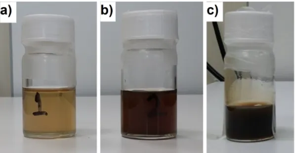
DMF solution. The ablation was carried out for 20000 cycles. 35 mL of silicon nanoparticle solution is obtained during each operation. Resulting solution is shown in Figure 2.1.
Figure 2.1: a) Photographic image of the silicon nanoparticles which were syn-thesized by laser ablation
2.2.2
Electrospinning of Silicon & Carbon Nanofiber
Composite
In preparation of silicon & DMF solutions, commercial silicon nanoparticles (SiNP), and concentrated solutions (SiNPA1, SiNPA2), which were prepared by evaporating a portion of DMF solvent at 60◦C for 2-3 days, were used. In densifi-cation of SiNPA1, DMF in 35 mL of silicon nanoparticle solution was evaporated to yield a 15 mL solution. Highly dense SiNPA2 solution was obtained by re-ducing the volume of DMF from 105 mL to 7.5 mL. Finally, the solutions were sonicated for 30 minutes before mixing them with the polymer precursor.
Figure 2.2: Photographic image of the silicon nanoparticle & PAN solutions with a) Silicon nanoparticles as synthesized, b) SiNPA1 and c) SiNPA2
The bead-free and uniform silicon & carbon nanofiber composite materials were produced by using DMF as solvent. The homogenous electrospinning so-lutions were prepared by dissolving PAN in silicon & DMF solution in different percentages, and magnetically stirring for two days at room temperature (see Figure 2.2). It was observed that below 8% PAN content, homogeneity in the fibers was lost (see Figure 2.3).
Figure 2.3: Photographic image of bead formation in inhomogeneous electro-spun fibers after carbonization, which contains 6 % PAN in its electrospinning precursor
Figure 2.4: Schematic representation of homogeneous electrospinning silicon nanoparticles & carbon nanofiber composite
Table 2.1: Parameters and proportions used in electrospinning precursor prepara-tion and electrospinning (The ”*” values are unknown since yield of the synthesis procedure was not clear)
Electrode Name SC1 SC1’ SC2 SC3 SC4 SC5 Si Precursor - - SiNP SiNPA1 SiNPA1 SiNPA2
%wt of PAN 10 8 10 10 8 8
Si:PAN ratio 0 0 1:6 * * *
Potential (kV) 15 12 15 15 12 12 Needle distance (cm) 15 15 18 18 15 18 Flow rate (ml/h) 0.75 0.75 0.75 1 0.85 0.5
Figure 2.5: Photographic image of the electrospun fibers
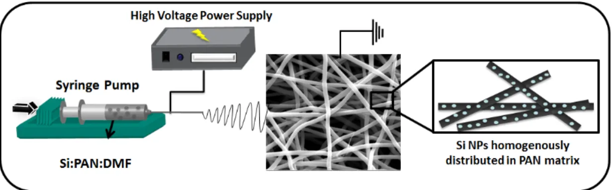
After clear solutions were obtained, they were loaded in syringes, which had metallic needle tips with 0.6 mm inner diameter. The syringes were positioned horizontally on a syringe pump (model KDS-101, KD Scientific, USA). One of the electrodes of high-voltage power supply (Spellman, SL30, USA) was clamped to the metallic needle. On the other side, plate aluminum collector, which was the substrate for fiber deposition, was grounded (see Figure 2.4. The processes were carried out at ∼25◦C and ∼20% relative humidity. The collected nanofibers were dried over night at room temperature in a fume hood. The electrospinning parameters and the solution proportions are given in Table 2.1. Furthermore, a representative picture of the electrospun fibers is given in Figure 2.5.
2.2.3
Heat
Treatment
Steps
of
Silicon
&
Carbon
Nanofiber Composite
Stabilization of the electrospun fibers was obtained by heating the samples to 280
◦C with 5◦C/min heating rate, then leaving the sample at the high temperature
for 2 hours. The stabilization procedure took place in open atmosphere. Later on, the samples were heated to 800 ◦C with 5 ◦C/min heating rate, and similar to the stabilization, they were held for 2 hours. Continuous argon flush was applied after the stabilization. In Figure 2.6, an image of electrospun fibers after carbonization was shown.
Figure 2.6: Photographic image of the electrospun fibers after carbonization
2.2.4
HF treatment of SC5
To remove the oxide layer on the silicon nanoparticles of SC5, 0.1 M HF solution was employed. Carbonized samples were dipped into the HF solution, and kept in the solution for 5 minutes. Afterwards, the samples were collected and dipped into DI water, and kept for 1 minute. The procedure with DI water was repeated twice. For further purification, the samples were put in ethanol for 5 minutes and then dried in vacuum oven overnight.
2.2.5
Thin Film Deposition of Aluminum and Aluminum
- Copper
Aluminum and aluminum - copper thin films were deposited on stainless steel (SS) substrates by VAKSIS NanoD-4S RF magnetron sputtering system using RT and RT - DC, respectively. Prior to deposition, SS substrates were cleaned with acetone, ethanol and DI water, subsequently. The depositions took place at room temperature and 20 mTorr pressure with 50 sscm constant Ar flow while 50 mm of constant target-to-substrate distance was maintained. 320 nm of aluminum was continuously deposited using an RF power of 125 W. For the deposition of aluminum - copper alloy, both DC and RF sources of the sputtering system were exploited to avoid air exposure and oxidation. To maintain 4 wt% copper ratio, required copper thickness on the substrate was calculated to be 4 nm. To prevent exposure of the thin copper layer, it was sandwiched between two aluminum layers, whose thicknesses were 160 nm each. During the deposition, the same parameters, which were previously indicated in the aluminum deposition, were applied for aluminum with RF source while a DC power of 150 W was hired for copper deposition.
2.2.6
Heat Treatment Steps of Aluminum and Aluminum
- Copper
Aluminum - copper thin films were heated to 540 ◦C with 5◦C/min heating rate using a tube furnace, and held there for 2 hours in open atmosphere. Then, the samples were quenched by using ice - DI water solution. Aging process was started when the temperature of the samples reduced to room temperature. For aging, the samples were heated to 170 ◦C with 5 ◦C/min heating rate using the same tube furnace, and held there for 14 hours in open atmosphere. Afterwards, they were left to cool at room temperature. To compare the effect of the heat treatment process, some of the aluminum thin film samples were also put through
Figure 2.7: Photographic image of (from left to right) SS, aluminum thin film after deposition, aluminum - copper thin film after deposition, aluminum - copper alloy after age hardening
thin films after deposition, and age hardened aluminum - copper alloy are shown in Figure 2.7.
2.2.7
Characterization
Different tools such as FEI Tecnai G2 F30 Transmission Electron Microscopy (TEM), FEI Quanta 200 FEG Environmental Scanning Electron Microscope (SEM), Thermo Scientific X-ray Photoelectron Spectrometer (XPS) using Al Kα radiation, PAN analytical XPert X-ray Diffractometer and PRO MRD diffrac-tometer using Cu Kα radiation (XRD and GIXRD, respectively), TA Instru-ments TGA Q500 (TGA) using dry air (H2O <1.5 ppm), and WITEC Alpha 300
Raman Microscope using a laser with 532 nm wavelength were exploited for the characterization of the electrode materials.
For characterization of silicon nanoparticles after the synthesis, DMF solution that contained the nanoparticles were dropped over copper and silica substrates in XPS, Raman Spectroscopy, respectively. For TEM measurements, the solution
was diluted with acetone to yield 5:1 acetone:solution ratio, then dropped over a film carbon grid and dried in oven at 60◦C and open atmosphere for a couple of minutes. Furthermore, for TG measurements, previously carbonized materials were used.
To characterize the electrodes after electrochemical testing, the batteries were carried in and disassembled in glovebox. The electrodes were washed with 3 mL acetonitrile to clean electrolyte residues. To avoid their contact with air, they were sealed in glovebox and then moved to instruments.
2.2.8
Lithium - Ion Battery Preparation
The electrode materials were vacuum dried at 70◦C overnight, then rapidly put into argon filled glovebox (O2 <0.5 ppm, H2O <0.5 ppm) to prevent air exposure.
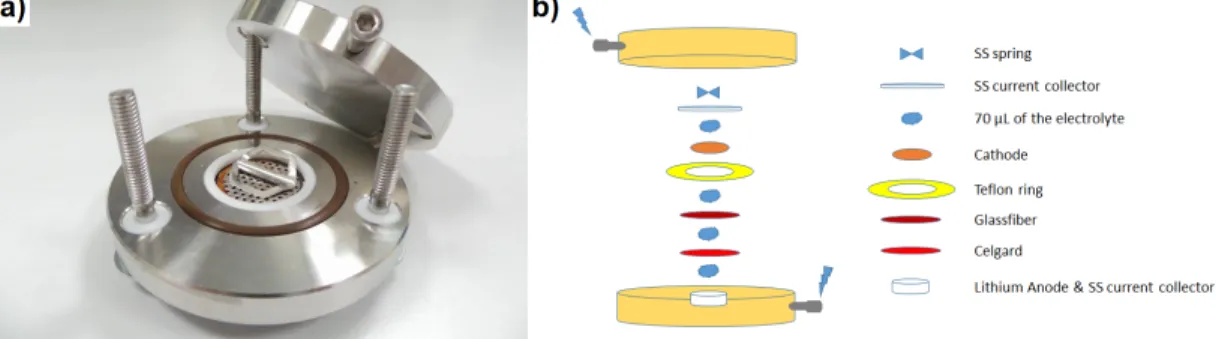
Swagelok type cells were used to build lithium half cells where lithium metal electrodes were used as anode materials (see Figure 2.8). Stainless steel current collectors were hired for both electrodes. Celgard C480 separators were utilized at anode while separators of the cathodes were glass microfiber filter (GF/C). The electrolyte solutions of the cells were composed of 280 µL of 0.5 M LiTFSI dissolved in EC:DMC (1:1) solution. The cells were sealed after the assembly to prevent interaction with the atmosphere, and rested at room temperature for 11 hours prior to testing.
Figure 2.8: a) Photographic image of the Swagelok battery cell b) Schematic representation of the components in the battery assembly
2.2.9
Electrochemical Characterization
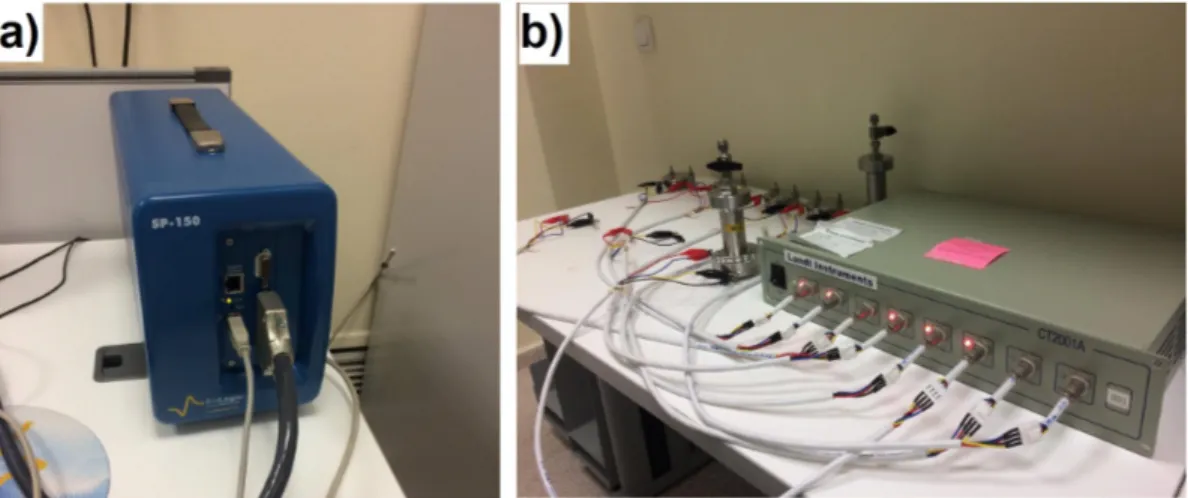
Biologic Instruments SP - 150 Potentiostat was hired for CV and impedance measurements of all the samples (see Figure 2.9a). For the aluminum samples, 0.5 mV/sec of scan rate was applied between 0.01 V - 1.5 V. For the silicon & carbon nanofiber composite electrodes, same potential interval was used, however, the scan rate was determined to be 0.1 mV/sec to differentiate the peaks of silicon and carbon. Furthermore, for impedance measurements of the silicon & carbon nanofiber composite electrodes, a frequency interval of 0.01 Hz to 1 MHz was hired at OCV, with 10 mV potential oscillation amplitude.
For the galvanostatic measurements, Landt CT2001A multichannel potentio-stat/galvanostat was employed (see Figure 2.9b). Different current rates (100 mA/g, 200 mA/g, 500 mA/g and 1000 mA/g) were applied to all the samples in the voltage range of 0.01 V - 1.5 V.
For the aluminum samples, the sequence for galvanostatic measurements was as follows: 10 cycles at 100 mA/g, 50 cycles at 200 mA/g, 10 cycles at 100 mA/g, 10 cycles at 200 mA/g, 10 cycles at 500 mA/g, and 10 cycles at 1000 mA/g. For the aluminum - copper alloy, 10 additional cycles at 100 mA/g were applied after the tests were finished.
Sequence for the silicon & carbon nanofiber composite electrodes was altered to observe their rate capability behavior earlier than their cyclic stability like the following: 10 cycles at 100 mA/g, 10 cycles at 200 mA/g, 10 cycles at 500 mA/g, and 10 cycles at 1000 mA/g, 10 cycles at 100 mA/g, and 50 cycles at 200 mA/g.
Average electrode weights for the aluminum samples were 0.1 mg - 0.2 mg while it was ∼1.3 mg for the silicon & carbon nanofiber composite.
Figure 2.9: Photographic image of a) Biologic Instruments SP - 150 potentiostat, and b) Landt CT2001A multichannel potentiostat/galvanostat
Chapter 3
Silicon Based Anode Materials
for Li - ion Batteries
In this chapter, fabrication and characterization of silicon carbon nanofiber com-posite anode materials were presented and discussed after introducing silicon as an anode material for lithium - ion batteries. The methods that have been used through out the study were also explained.
3.1
Silicon as an Anode Material for Lithium
-Ion Batteries
Silicon is a very popular alloying based anode material for lithium - ion batteries as mentioned previously. In addition to being the second most abundant element on the earth, it also offers a very large capacity. After full lithiation, Li15Si4
(yielding 3579 mAh/g theoretical capacity) and Li22Si5 (yielding 4200 mAh/g
theoretical capacity) alloys are formed at room temperature and at 415 ◦C, re-spectively. [57]. Furthermore, it offers a very high energy density provided that it has an average discharge potential of ∼370 mV vs. Li/Li+ [58].
Thermodynamically, silicon should go through a series of phase transforma-tions before it ends up with fully lithiated state as follows: Si to Li12Si7, Li12Si7
to Li14Si16, Li14Si16 to Li13Si4 and Li13Si4 to Li22Si5. In practice, these
trans-formations are only observed as multiple potential plateaus at elevated tempera-tures (i.e. 450 ◦C) while at room temperature, crystalline silicon is transformed into amorphous silicon at ∼100 mV vs. Li/Li+ and continues cycling in that state [59, 60]. Furthermore, formation of metastable Li15Si4 phase is observed
under 50 mV potential vs Li/Li+ upon lithiation [61].
The problems related to employing silicon as electrode material could be in-dicated in three main topics: Low intrinsic electrical conductivity, pulverization and electrical contact loss, and unstable SEI formation.
Firstly, silicon is well - known for its semiconducting electrical properties. When electric conductivity of an electrode material is low, it gives rise to over-potential, which is especially pronounced at high current rates. Energy efficiency of an electrode is dramatically reduced in presence of a large overpotential.
Secondly, high lithium uptake of silicon cause large volume changes (∼400%) during lithiation and delithiation, forming massive stresses. As a result, crack formation is observed in bulk silicon, even during first electrochemical cycles. Those cracks then lead to loss of electrical contact with current collector and within the electrode, eventually form inactive dead weight. This phenomenon is referred to as pulverization, and it is partially responsible for capacity loss in silicon anodes [62]. On the other hand, electrical contact loss does not always occur due to cracking. While volume of silicon contracts during delithiation process, some particles can lose their contact with each other and some gaps can form between them, which has similar consequences with pulverization [33].
Finally, it is important for SEI film to be stable for electrode materials as mentioned previously. In the literature, it was confirmed with HRTEM, FTIR, and XPS that SEI films in silicon electrodes are composed of Li2CO3, Li2O, LiF,
is that because of the pulverization problem mentioned above, new surfaces are exposed to electrolyte upon cycling. Thus, SEI formation proceeds and leads to continuous capacity loss.
To circumvent these challenges, different applications of nanotechnology were hired. First and foremost, reducing size increases surface to volume ratio, enhance electric conductivity, and shorten diffusion distances of lithium ions [67]. One could consequently obtain an electrode with lower overpotential, better rate ca-pability, and higher capacity. Furthermore, nanoparticles are less prone to stresses formed due to volumetric changes. In a study, it was proposed that particles with lower diameter than 10 nm would not experience pulverization according to the calculation of misfit stress energies of partially delithiated (lithiated core - delithi-ated shell) particles with different sizes [68]. Although nanoengineering enhances general properties of an electrode; stability, reversibility and energy density of an electrode are highly dependent on nanostructure. Various morphologies were investigated in the literature such as nanoparticles, nanotubes, porous spheres, core - shell structures, and nanocomposite structures etc.
As mentioned above, silicon nanoparticles could withstand large volumetric strains upon cycling; however, supplying and keeping electrical connection with current collector and within electrode stands a problem [69]. Convensional slurry methods including conductive carbon and binder addition did not prove effective for silicon. Therefore reaching the full capacity and cyclic stability is problematic for the nanoparticles. Silicon nanowires, on the other hand, are advantageous over the nanoparticles as they provide one - dimensional electronic pathways and each of them are connected to current collector. Hence, they supply robust electric conductivity without requiring usage of conductive additive or binder. Furthermore, the empty space between neighbour nanowires enable accomodation of volume changes upon cycling. Combination of advances in electric conductivity and buffer zone for volumetric change enhances capacity and cyclic stability of silicon nanowires. In the literature, core - shell nanowire structures, where core is an electrically conductive layer and shell is electrochemically active silicon, with increased rate capability and cyclic stability were also reported [64]. On the other
in nanoparticles. Silicon nanoparticles are coated with amorphous carbon, which helps buffering volumetric changes and provide electrical conductivity. Moreover, it prevents direct contact of electrolyte to silicon, and forms a more stable SEI [70,71]. It is also possible to form a structure with more than one shells to increase the material’s properties. Luo et al. reported that they synthesized a core -shell - -shell nanoparticle structure with silicon - amorphous carbon - crystalline TiO2, respectively [62]. Crystalline TiO2 was used to form a better SEI layer
and improve mechanical properties of the nanoparticles. Additionally, thin film silicon anodes were also tested at the initial stages of silicon research [72]. The advantage of thin films is that the critical fracture stress is inversely proportional to the film thickness according to the Griffith - Irwin relation [68]. Although some cracks are observed after initial cycle, capacity fade is comparatively lower than bulk silicon since cracked particles are still attached to current collector [73].
3.2
Electrospinning
Electrospinning is a method to generate exceptionally long and uniformly thick one - dimensional nanofibers with solid or hollow interiors. With the method, it is possible to form nanofibers with various compositions. Electrospinning technique makes use of the uniaxial elongation of a polymer solution or melt, which acts as a viscoelastic jet. Instead of hiring mechanical force for elongation, electrostatic repulsion, which is obtained by applying a potential difference between two sur-faces, is exploited. When compared to mechanical drawing, electrospinning can provide much thinner fibers (considerably thinner than a human hair) [74, 75]. It is particularly useful in electrode preparation as it is possible to form silicon & carbon nanofiber composites by simply combining polymer solution and silicon containing solution, then using the mixture as electrospinning precursor. Elec-trospun composites combine the advantages of size reduction with stability and conductivity of carbon nanofibers throughout the electrode.
3.3
Silicon & Carbon Nanofiber Composite
Having mentioned different morphologies for silicon anodes, electrospinning of-fers some advantages in electrode formation as it is a simple, cheap, and scalable method for continuous silicon containing nanofiber production. Furthermore, electrospun electrodes are composed of free - standing, ductile and conductive nanofibers. They do not require conductive additive or binder addition to be used as electrodes. Furthermore, the fact that they are able to free - stand elim-inates the requirement of slurry preparation. There are different morphologies of electrospun silicon & carbon nanofiber composites reported in the literature such as continuous, core - shell, and porous structures [76–81]. Generally, commer-cial silicon nanoparticles having diameter of ∼50 - 100 nm are employed in the composites.
In the continuous nanofibers, silicon particles are partially exposed to elec-trolyte due to their large size, which results in SEI formation and capacity loss upon cycling. In a continuous nanofiber composite study, commercial silicon nanoparticles (∼50 nm size) and PAN solution were electrospinned and then car-bonized [81]. An initial specific discharge capacity of 1620 mAh/g and Coulombic efficiency of 66.6% were obtained at 0.1 C current rate in a potential range of 0.01 V to 1.5 V. It was reported that after 100th cycle, 850 mAh/g of capacity was obtained with 52.5% capacity retention.
In the core - shell structures, various type of studies were conducted. Xiao et al. suggested a structure which is composed of PVDF membrane core. On top of that, a conductive inert nickel shell and electrochemically active amorphous silicon shell were coated via aqueous electroless plating and magnetron sputter-ing, respectively [76]. In their galvanostatic measurements, they preferred to use 0.05 V - 1.2 V potential interval vs Li/Li+. Their anode yielded 3210 mAh/g initial specific discharge capacity at 0.2 C while the capacity was reduced to 1821 mAh/g after 1000 cycles, providing 56.9% capacity retention. In a different ex-ample, a core - shell - shell structure (using PAN - silicon - PAN precursors, respectively) was designed by dual nozzle co - axial electrospinning, which was
followed by carbonization [77]. In half cell measurements between 0.01 V - 3 V potential range, their electrode provided 1479.8 mAh/g specific discharge capac-ity with 82.7% Coulombic efficiency at 50 mA/g current rate. After 50 cycles, their capacity was decreased to 886.5 mAh/g with a capacity retention of 72.4% capacity retention.
Porous fiber electrodes, on the other hand, provide larger surface area, shorter Li+ ion diffusion path and increased silicon content to the composite. In an
example, Li et al. proposed electrospinning silicon nanoparticles with PAN and PMMA precursor [80]. After carbonization, PMMA leads to formation of pores in the structure. Their electrode offered 3109 mAh/g first overall discharge capacity with 61% Coulombic efficiency when the half cell was cycled in between 0.05 V -1.2 V at 0.05 C current rate. A discharge capacity of 950 mAh/g was obtained 80th cycle with 30.6% capacity retention.
In this study, we aimed to propose a free - standing, cheap and scalable con-tinuous silicon & carbon nanofiber composite electrode with high capacity and stability. To do that, we synthesized smaller silicon nanoparticles than what were used in previously reported studies with different synthesis routes, then we homo-geneously embedded and distributed the particles inside the carbon nanofibers. With the help of size reduction, we tried to achieve complete coating of the par-ticle to prevent electrolyte exposure, buffer the volumetric changes, and enhance the ion diffusion kinetics. Polyacrylonitrile (PAN) was determined to be the poly-mer source as it is a frequently used polypoly-mer in electrospinning and its carbon yield after carbonization is relatively higher than other polymers. Furthermore, we avoided to use metal or metal - oxide coating to decrease the cost and enhance the ease of production.
3.4
Results & Discussion
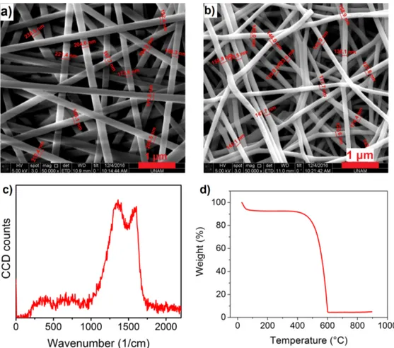
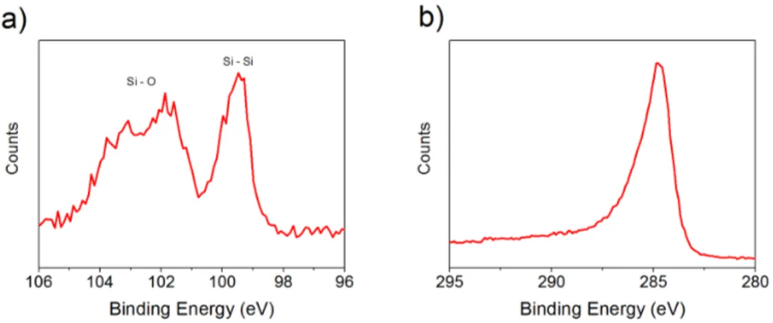
Figure 3.1: a) Regional XPS scan for Si 2p of, b) Raman spectra of, c) TEM image of silicon nanoparticles, which are synthesized via laser ablation
Figure 3.2: Regional XPS scans for a) C 1s, b) O 1s, c) N 1s of SC1 before carbonization (black), and after carbonization (red)
Figure 3.1a represents regional XPS scan for Si 2p of silicon nanoparticles, which were synthesized via laser ablation. According to the results, there are two peaks located at 103.5 eV and 99.4 eV, which came from silicon in silica and Si NPs, respectively. Since XPS is a surface characterization technique, and peak intensity of Si - O bond is respectively higher than peak intensity of Si - Si bond, it was concluded that silicon core is coated with a silica layer, which has a few nm thickness. Presence of silicon was further proven with Raman spectroscopy, see Figure Figure 3.1b. The only peak that was observed lies between 500 cm−1 and 530 cm−1, which is the strongest characteristic peak of silicon [82]. In Figure 3.1c, TEM image of the synthesized silicon nanoparticles having ∼20 nm average size were shown. In high - resolution TEM mode (see Figure A.1a), it was observed that the particles contain crystalline silicon cores, which were surrounded by a
Regional XPS scan for C 1s of only carbon nanofiber (CNF) electrode (SC1) was given in Figure 3.2a. It was noticed that intensity of the peak at 284.8 eV, which corresponds to graphitic carbon, was increased after carbonization while the peak at 285.5 eV, which indicated C in C = N groups, was diminished. Oxygen peak, which is located in between 532 eV - 533 eV, signifies the presence of organic C - O and C = O groups in the fibers, and its intensity was slightly increased after carbonization, see Figure 3.2b. It was probably originated from functional groups, which were formed during the stabilization process of the fibers before carbonization. Finally, in Figure 3.2c, it was observed that the nitrogen peak diminished after carbonization, indicating that the nitrogen groups were almost fully eliminated. It was inferred from the XPS results that the carbonization of the fibers was successfully achieved.
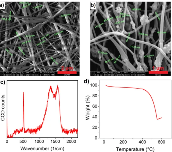
When SEM images of SC1 before and after carbonization were investigated, it was concluded that the fibers were homogeneously electrospun, see Figure 3.3a and 3.3b. Diameter of the fibers before carbonization was 198∓18 nm while after carbonization the diameter was decreased to 140∓15 nm. A reduction was expected in the volume as well as the weight due to decomposition of side groups and loss of nitrogen. The Raman spectrum in Figure 3.3c demonstrates both the D band (1440 cm−1) and the G band (1580 cm−1), which indicates that the fibers were partially transformed into amorphous carbon, and there were some defects on their structure. Since the carbonization temperature (800◦C) was not too high, total carbonization of the fibers was not anticipated. Furthermore, TG analysis of the fibers indicate that almost all the material was burned at 600 ◦C in presence of O2, as predicted, see Figure 3.3d.
Figure 3.3: SEM images of SC1 a) Before carbonization, b) After carbonization, c) Raman spectrum and d) TG curve of SC1
Regional XPS scan for Si 2p of SC2 in Figure 3.4a reveals that commercial silicon nanoparticles were present with carbon nanofibers to form a composite. There is a peak located at 99.4 eV, which came from silicon in the nanoparticles. Furthermore, the peaks, which are distributed in between 101 eV and 105 eV, indicate that there is a SiOxlayer around the nanoparticles. The graphitic carbon
peak located at 284.8 eV proves that the structure was not affected after the silicon addition, see Figure 3.4b.
In Figure 3.5a, it was observed from the SEM image that the homogeneity of the fibers was lost after commercial silicon nanoparticle addition. Diameter of the fibers varied from ∼100 nm to ∼250 nm and some beads were visible. Af-ter carbonization, the fiber diameAf-ter was reduced to ∼100 nm, see Figure 3.5b.
Figure 3.4: Regional XPS scan of SC2 for a) Si 2p and b) C 1s, after carbonization
in size, were observable on top of the fibers. The inhomogeneity in particle dis-tribution and the particle agglomeration were expected to cause critical drop in performance of the electrodes. Presence of the nanoparticles after carbonization was further proven by using Raman spectrum as shown in Figure 3.5c. Charac-teristic silicon peak at ∼520 cm−1 was present along with the D and the G bands in the spectrum. Similarity of the D and the G bands of this spectrum to the spectrum of SC1 supports preservation of the amorphous carbon structure with the silicon addition. According to the TG curve of SC2, the nanoparticle content was measured to be ∼35 wt%, see Figure 3.5d. Increase in the weight after ∼600
◦C was due to further oxidation of the nanoparticles.
Regional XPS scans in Figure 3.6 show the effect of changing parameters during the electrospinning process. It was noted that the signal coming from silicon in Si NPs at 99.4 eV was not observable in the regional scans for Si 2p (Figure 3.6a), although it was detected in XPS measurements of the silicon nanoparticle precursor solution (Figure 3.1a). Since XPS is a surface analysis technique, it was inferred that the nanoparticles were embedded inside the fibers, rather than being deposited on their surfaces. Thus, only the oxide layer of the particles was detected in between 101 eV and 105 eV. Furthermore, decreasing PAN ratio in the electrospinning precursor solution from 10% to 8% seemed to increase intensity of the signal coming from silicon, which was anticipated as the fiber thickness
Figure 3.5: SEM images of SC2 a) Before carbonization, b) After carbonization, c) Raman spectrum and d) TG curve of SC2
for the electrospinning precursor seemed to boost the silicon signal intensity one step further in SC5, which was quite anticipated. According to regional scans for C 1s in Figure 3.6b, however, there was no difference in the amorphous carbon structure of the fibers if the amount of silicon or PAN precursor were changed.
Findings of XPS measurements were further supported by SEM, see Figure 3.7a, 3.7b and 3.7c. There was no agglomeration of silicon nanoparticles on the fiber surfaces unlike the observations made in SC2 (Figure 3.5b), so it was con-firmed that the particles were embedded inside the fibers. Furthermore, diameter of the fibers in SC3, which was 315∓49 nm, was comparatively higher than the
Figure 3.6: Regional XPS scans of SC3 (black), SC4 (red) and SC5 (blue) for a) Si 2p and b) C 1s
Figure 3.7: SEM images (after carbonization) of a) SC3, b) SC4, and c) SC5
value of SC2. The increase was affiliated with decreasing silicon - to - carbon ra-tio. On the other hand, fiber diameter was reduced to 133∓22 nm in SC4, when the PAN content of the precursor solution was decreased from 10% to 8%, which could help enhancing the electrode’s total gravimetric capacity by increasing its silicon - to - carbon ratio. In addition, SC4 seems to be denser than SC3, which could also contribute to the electrode’s overall volumetric capacity. Nevertheless, fiber connection in SC4 seemed to have some disconnections and distortions in its structure, which could cause electric conductivity problems especially at high current rates. Similar structural distortions were also observed in SC5 (see Fig-ure 3.7c). An increase was observed in the fiber diameter to yield 162∓22 nm. The increase was associated with the increasing silicon content due to the more
SC5. It was noted that the silicon - to - carbon ratio was inversely proportional with the fiber thickness up to some critical point, which was then followed by a proportional relation. Furthermore, some particles were noticable close to the fibers’ surface, which is in correlation with the XPS results as intensity of the silicon was increased in SC5.
TG curves of SC3 and SC4 were given in Figure 3.8. According to the curves, 5.9 wt% and 6.3 wt% of the materials remained after ∼600◦C, respectively. Only 0.4 wt% difference was observed between SC3 and SC4. Hence, it was noted that although the fiber diameter was decreased to almost half when the PAN content in the precursor was reduced from 10% to 8%, it did not effect the silicon to -carbon ratio, dramatically. Furthermore, it was anticipated that these electrodes cannot provide high lithium storage capacities due to their low silicon content.
Figure 3.8: TG curves (after carbonization) of a) SC3, b) SC4
TG curve of SC5 was given in Figure 3.9a, which indicated that amount of TGA remnant in this material was 16.9 wt% at ∼600 ◦C. When it was compared to amount of the remnants of SC3, 10.6 wt% of increase was calculated in SC5. It was inferred from the results that when the silicon solution was densified prior to mixing with the electrospinning solution, along with decreasing the PAN content of the precursor solution from 10% to 8%, it was possible to enhance the silicon content of the materials, greatly. Nevertheless, amount of silicon was measured to be inferior than the value observed for SC2 (see Figure 3.5d). To have a
Figure 3.9: TG curves of a) SC5 after carbonization, b) SC5 after HF treatment
embedded in the fibers of SC5, another TGA was performed for HF - treated SC5, and the result was presented in Figure 3.9b. After the oxide layer was etched, amount of the remnants was calculated to be 7.9 wt%, which corresponded to almost half the value of the pristine sample. Hence, it was concluded that approximately half of the particles consisted of SiOx layers.
Further characterization steps were performed on HF treated SC5 to reveal effect of HF to the material structure. High shift in silicon peak to lower binding energy (see Figure A.2a) indicated that elimination of the oxide layer was suc-cessfully achieved. Small deviation in the peak from the Si0 peak at 99.4 eV was considered as an effect of size reduction, where presence of surface atoms start to dominate the structure and alter the bonding energy. While there was no difference between the carbon peaks after the HF treatment (see Figure A.2b), Figure A.2c represented presence of F on the surface after the treatment. Fur-thermore, SEM images of the sample showed correlation with the XPS results, where there was no visible damage on the fibers (see Figure A.3a, and presence of F was confirmed with EDS in Figure A.3b. Moreover, lack of oxygen peak in EDS additionally proved elimination of the oxide layer.
Figure 3.10 presents regional XPS scans for Si 2p and C 1s of SC5 before TG analysis, and remnants of SC5 after the analysis. Expectedly, signals coming
Figure 3.10: Regional XPS scans of SC5 before (black), and after (red) TGA for a) Si 2p, and b) C 1s
in the material were fully oxidized and resulted in forming a peak at 103.5 eV, which indicates presence of silica. Carbon in the material, on the other hand, was almost fully oxidized and evaporated since the intensity of carbon peaks reduced dramatically, see Figure 3.10b. Oxidization of carbon was further confirmed with the peak with a small intensity, which was formed at ∼288.5 eV and came from C in O - C = O groups.
Structure of the carbonized SC5 was investigated further with Raman spec-troscopy, see Figure 3.11. Characteristic peak of silicon was almost fully dimin-ished at ∼520 cm−1. It was inferred that either the laser could not reach to the embedded particles or signal coming from the particles was lost in the back-ground. Ratio of D band to G band was observed to be comparatively higher than the ratios for SC1 and SC2, which indicated that there were more defects in fiber structure of SC5 than the other samples. Hence, it was expected for SC5 to perform poorer at high current rates.
Figure 3.12: Cyclic voltammograms of a) SC1, b) SC2, and c)SC5, where the first, the second and the third cycles were indicated with black, red, and blue, respectively
According to cyclic voltammograms, SC1 showed a cathodic peak at ∼0.7 V, which corresponds to irreversible SEI layer formation (see Figure 3.12a). After the peak, the current started to increase at ∼0.4 V and showed no individu-ally observable peak, which was due to the homogeneous insertion mechanism of amorphous carbon. Furthermore, similar behaviour was observed during the oxidation. In the following cycles, reversibility of the electrochemical reaction was increased as area of the cathodic region gradually decreased and got close to the value of the anodic region. In the voltammogram of SC2 (see Figure 3.12b) showed a different SEI formation profile in its first cycle, where there was no peak to single out. It was inferred that presence of the commercial silicon nanoparti-cles, which was composed of differently sized partinanoparti-cles, on surface of the fibers led to formation of SEI at different potentials. Two cathodic peaks were observed in the first cycle at ∼0.2 V and ∼0.1 V. The peak at ∼0.1 V indicated transition of crystalline silicon to amorphous silicon; however, origin of the peak at ∼0.2 V was
cycles. Moreover, anodic peak at ∼0.5 V arose from delithiation of amorphous silicon - lithium alloy, whose intensity was continuously raised upon following cycles. Along with the decreasing area of the cathodic side, it was noted that reversibility of the reaction increased gradually. Figure 3.12c shows the voltam-mogram of SC5, where SEI formation exhibited a similar profile to SC1’s. In addition, presenting no sharp cathodic peak suggested a homogeneous insertion mechanism like SC1. On the other hand, an anodic peak with a small intensity was emerged in the second cycle at ∼0.5 V. Thus, it was concluded that a small activation of the silicon in the structure was obtained. Lastly, reversibility of the reactions was increased gradually, just like the previous electrodes.
Figure 3.13: Galvanostatic charge/discharge curves of a) First 10 cycles at 100 mA/gcathode, b) Last 10 cycles at 100 mA/gcathode, c) Cyclic stability
measure-ment at 20 mA/gcathode between 40th and 90th cycles, and d) Rate capability
measurement between 10th and 40th cycles, of SC1
Electrochemical characterization of electrode materials were further performed galvanostatically, see Figure 3.13. A huge SEI layer formation was observed in