PROCEEDINGS OF SPIE
SPIEDigitalLibrary.org/conference-proceedings-of-spie
Gibbs free energy assisted
passivation layers
Omer Salihoglu, T. Tansel, M. Hostut, Y. Ergun, A.
Aydinli
Omer Salihoglu, T. Tansel, M. Hostut, Y. Ergun, A. Aydinli, "Gibbs free
energy assisted passivation layers," Proc. SPIE 9819, Infrared Technology
and Applications XLII, 98190R (20 May 2016); doi: 10.1117/12.2223389
Event: SPIE Defense + Security, 2016, Baltimore, Maryland, United States
Gibbs Free Energy Assisted Passivation Layers
Omer Salihoglu
a,*, T. Tansel
b, M. Hostut
c, Y. Ergun
d, and A. Aydinli
aa
Department of Physics, Bilkent University, 06800 Ankara, Turkey
bInstitute of Nuclear Sciences, Hacettepe University, 06532 Ankara, Turkey
c
Department of physics Education, Akdeniz University, 07058 Antalya, Turkey
d
Anadolu University, Department of Physics, Eskisehir, Turkey
ABSTRACT
Reduction of surface leakage is a major challenge in most photodetectors that requires the elimination of surface oxides on etched mesas during passivation. Engineering the passivation requires close attention to chemical reactions that take place at the interface during the process. In particular, removal of surface oxides may be controlled via Gibbs reactivity. We have compared electrical performance of type-II superlattice photodetectors, designed for MWIR operation, passivated by different passivation techniques. We have used ALD deposited Al2O3, HfO2, TiO2, ZnO, PECVD deposited SiO2, Si3N4 and sulphur containing octadecanethiol (ODT) self-assembled monolayers (SAM) passivation layers on InAs/GaSb p-i-n superlattice photodetectors with cutoff wavelength at 5.1 µm. In this work, we have compared the result of different passivation techniques which are done under same conditions, same epitaxial structure and same fabrication processes. We have found that ALD deposited passivation is directly related to the Gibbs free energy of the passivation material. Gibbs free energies of the passivation layer can directly be compared with native surface oxides to check the effectiveness of the passivation layer before the experimental study.
Keywords: Superlattice, Photodetector, InAs/GaSb, ALD, Gibbs Free Energy, Passivation
1. INTRODUCTION
Photodetectors with dry or wet etched mesa side walls often lead to increased surface leakage currents that degrade detector performance and Type II InGaAs/GaSb superlattice (T2SL) photodetectors operating in MWIR and LWIR regions are no exception. Type-II InAs/GaSb superlattices has recently gained a lot of interest for the infrared photodetector applications due to many advantages like suppression of Auger recombination [1], and interband tunneling [2], and the ability to tailor the bandgap within most of the infrared region by changing the thickness of the constituent InAs and GaSb layers [3]. InAs/GaSb superlattices are periodic structures consisting of alternating layers of nanometers thick InAs and GaSb layers. Surface passivation is extremely critical in T2SL InAs/GaSb photodetectors, due to large number of very thin alternating layers. Different etch rates of InAs and GaSb during mesa definition lead to roughness on the mesa side walls. A conformal coating can be critical to cover all the tiny undulations on mesa side walls. Furthermore, components of InAs/GaSb SL are chemically very reactive. They are easily oxidized and a native oxide layer of several nanometers thick is quickly formed upon exposure to air. Adsorbed oxygen diffuses through the surface, reacts with Ga, Sb, In and As atoms then forms native oxides such as Ga2O3, Sb2O3, In2O3, As2O3 and InAsO3 some of which are conductive [4,5].
*[email protected]; phone +90 (262) 677 2797
Infrared Technology and Applications XLII, edited by Bjørn F. Andresen, Gabor F. Fulop, Charles M. Hanson, Paul R. Norton, Proc. of SPIE Vol. 9819, 98190R · © 2016 SPIE · CCC code: 0277-786X/16/$18 · doi: 10.1117/12.2223389
Proc. of SPIE Vol. 9819 98190R-1
Downloaded From: https://www.spiedigitallibrary.org/conference-proceedings-of-spie on 12/16/2018 Terms of Use: https://www.spiedigitallibrary.org/terms-of-use
This mechanism is responsible for the formation of additional conductive channels and consequently, leads to a large surface leakage. So far, many passivation techniques have been proposed to overcome these surface leakages. Dielectric material deposition [6, 7], sulfurization [8, 9], overgrowth with wide band gap materials [10] and polymer film coating [11] techniques can be listed as successful methods for passivation. Passivation is expected to limit oxidation of the side walls, saturate dangling bonds to avoid surface states and self clean [12] already formed native oxides at the etched surfaces. Sulfur containing solutions satisfies the dangling bonds and cleans the conductive native oxides by replacing the oxygen atoms with sulfur atoms. Although sulfurization is a very effective method, sulfur passivation does not have long term stability. In addition, sulfur solutions may damage the crystal surfaces causing losses in the optical performance. Dielectric deposition by plasma enhanced chemical vapor deposition (PECVD) is a very common technique in t industrial production of photodetectors but it may create plasma damage and thermal damage on the crystal structure. On the other hand, atomic layer deposited (ALD) metal oxides seem to satisfy all passivation needs by providing damage free, low stress, low interface state density and low pin hole density coatings. In this work, we have compared the electrical performances of type-II superlattice pin photodetectors to determine the effectiveness of ODT SAM passivation, PECVD grown SiO2 and Si3N4 passivation, ALD grown Al2O3, HfO2, TiO2 and ZnO passivation. Electrical performance of the photodetectors has been compared against unpassivated reference photodetectors to determine the effectiveness of the ALD deposited oxides. The same crystal structure and same fabrication processes were used to test different passivation materials.
2. EXPERIMENTAL
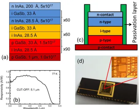
The SL structure was designed for MWIR operation with design cutoff wavelength of 5 µm. Figure 1a. illustrates structure of the p-i-n design type-II superlattice crystal design with corresponding thicknesses and doping concentrations. The pin part contains 140 periods 8 monolayers (MLs) of InAs/8 MLs of GaSb:Be (p=1.5x1017 cm-3) p-type layers, 40 periods 8 MLs of InAs / 8 MLs of GaSb i-layers, 60 periods 8 MLs of InAs:Te (n: 5x1017 cm-3)/8 MLs of GaSb n-type layers. 1000 nm GaSb:Be (p=1.0x1017 cm-3) and 20 nm InAs:Te (n: 5x1017 cm-3) layers introduced as p contact and n contact layers, respectively [13]. Figure 1b shows measured cut-off wavelength of the designed SL structure after optical response measurements which are done at 77 K by using a FTIR. Fotodetectors with mesa sizes from 100 x 100 µm2 to 700 x 700 µm2 are fabricated using phosphoric acid based solution (Figure 1c). Ohmic contacts were deposited by evaporating 5 nm titanium and 200 nm gold [14]. For ODT passivation, the sample was immersed in 1mM solution of ODT (Aldrich, 99%) in ethanol and was left in the solution for 48 hours at 60 0C. SiO
2 and Si3N4 films were coated in PlasmaLab 8510C reactor at 160 0C and the process was carried out under the pressure of 0.5 Torr and RF power of 9 W. Flow rates were 180 sccm SiH4 (%2 in N2), 225 sccm N2O for SiO2 and 45 sccm NH3 for Si3N4. Final thickness of the passivation layer was about 250 nm. Al2O3, HfO2, TiO2 and ZnO depositions carried out in atomic layer deposition system (Savannah 100) with 150 0C as the substrate holder temperature under constant 20 sccm N
2 gas flow. Growth of thin films have been done by delivering 0.015 s water vapor (H2O) and related precursor gas pulses into the chamber in a sequential manner. A wait time of 20 s was added after each pulse to ensure surface reactions to take place. 0.015 s trimethylaluminum (TMA), 0.15 s tetrakis (dimethylamido) hafnium (TDMAHf), 0.15 s tetrakis (dimethylamido) titanium (TDMATi) and 0.2 s dimethylzinc (DMZn) precursor gas pulses used for Al2O3, HfO2, TiO2 and ZnO film depositions, respectively. Passivated samples along with reference samples were bonded to a 40 pin dual in-line package (DIP) chip carrier for electrical measurements. Figures 1d shows image of the sample bonded to a 40 pin DIP chip carrier.
Proc. of SPIE Vol. 9819 98190R-2
Downloaded From: https://www.spiedigitallibrary.org/conference-proceedings-of-spie on 12/16/2018 Terms of Use: https://www.spiedigitallibrary.org/terms-of-use
n InAs, 200 A, 5x10¹⁷ I GaSb, 33A n InAs, 28.5 A, 5x10¹⁷ i GaSb, 33A i InAs, 28.5A , 1.5x10¹⁷ i InAs, 28.5A MiliSb, 1 pm, 1.0x10¹⁷
(a)
a 0.4 co K 0.2 080 CUT -OFF: 5(b)
Nm 3.5 4.0 45 Wavelength (µm) 5.0 55 x60 x60 (C) x90 n- contact n-type i-type p-type p- contactFigure 1: (a) structure of the p-i-n design superlattice crystal with corresponding thicknesses and doping concentrations. (b) Measured cut-off wavelength of the SL structure. (c) Schematic cross section of the InAs/GaSb SL p-i-n photodiode structure. (d) Image of the sample bonded to a chip carrier, inset shows close view of the bonded sample.
3. RESULTS AND DISCUSSIONS
Dark current and dynamic resistance measurements have been done at 77K to investigate electrical performance of the passivation layers. We have used unpassivated control samples along with passivated samples. The photodetectors were put into an aluminum box and immersed into liquid nitrogen filled container. HP4142OA source-measure unit has been used to measure dark current voltage-current characteristics of the samples. Figure 2 shows the measured dark current density vs. applied bias voltage characteristics of the unpassivated and passivated 400x400 µm single pixel test diodes at 77K. Dots show dynamic resistance area product (RA) vs. applied bias voltage for selected photodiodes. At -0.1 V reverse bias, dark current density is measured as 3.3 x 10⁻⁸ A/cm2, this measurement yielded RA product value of 2.5 x 10⁶ Ωcm2, for the Al
2O3 passivated photodetectors. Photodetectors passivated with a thin layer of Al2O3 shows the lowest dark current and highest dynamic resistance area product values for all bias voltages. Si3N4 is clearly the worst passivation material in this group. Photodetectors with ODT passivation show almost the same electrical characteristics with Al2O3 passivated photodetectors up to 0.1 V reverse bias beyond which the slope of the dark current increases when compared with detectors that are passivated with Al2O3. At low temperatures, currents in the photodetector are diffusion limited near zero bias. At larger biases, weak fluctuations in the already low current in ODT and Al2O3 are suggestive of trap assisted tunneling. Our results suggest that trap assisted currents are dominant for higher voltages for ODT passivation. Since the ODT chain is 2 nm long and the process is self-limited, some trap states on surface of ODT layer may still affect the electrical performance of the detector at high voltages through tunneling. Our electrical measurements show that Al2O3 passivation results in lower dark current than industry standard SiO2 passivation at the same temperature.
Proc. of SPIE Vol. 9819 98190R-3
Downloaded From: https://www.spiedigitallibrary.org/conference-proceedings-of-spie on 12/16/2018 Terms of Use: https://www.spiedigitallibrary.org/terms-of-use
Dark current density (A/cm2)
,o
o'
0 0
0 0 ó
0
0
ó o
0
OO-
O N O O ON Oo
W P OIDynamic resistance -area product (c2cm2)
10 1 0.1 0.01 1E-3 1E-4 1E-5 1E-6 1E-7 Si3N4 -- HfO2
--ZnO
--Si02
-0-Unpass. --ODT--TiO2
--AIO
2 3 5 10 15 20 25 1000/T (1 /K) 30 35Figure 2: Dark current density vs. applied bias voltage curves for passivated and unpassivated 400 x 400 µm diodes at 77K. Dots show differential dynamic resistance area product vs. applied bias voltage characteristics for selected diodes (same color coding).
Relationship between dark current densities versus inverse temperatures under 0.5 V reverse bias is shown in Figure 3. The temperature dependent I-V curve is dominated by diffusion current at high temperatures, generation-recombination current at mid temperatures and trap related currents at low temperatures. For temperatures lower than 70 K, all samples are dominated by surface related trap currents which give information about quality of the passivation. Al2O3 passivation results in at least an order of magnitude better performance than its closest competitor. This suggests that Al2O3 passivation reduces native oxides [12] eliminating surface states and preventing current flow through the surface channel. ODT and SiO2 passivated samples show almost the same performance in this voltage range. Arrhenius type behavior has been observed for all samples which is an indication of diffusion dominated behavior. Arrhenius type behavior yielded activation energies of approximately 0.23 eV which is close to the device band gap.
Figure 3: Temperature dependent dark current density for unpassivated and passivated type-II InAs/GaSb superlattice 400 x 400 µm photodiodes at -0.5 V bias voltage.
Proc. of SPIE Vol. 9819 98190R-4
Downloaded From: https://www.spiedigitallibrary.org/conference-proceedings-of-spie on 12/16/2018 Terms of Use: https://www.spiedigitallibrary.org/terms-of-use
10' io4
6 66
0M
0
c
á co
á
o
CD : G. mO
I .Q
I dark=Ibulk+IsurfaceÓ
a
_
~
'bulk 'surfaceo
CN
. : 1ir-1irbulk+1irsurfacela
450 -400 -350 -300 -250 -200 -150Gibbsfree energy (kcal /mol)
-100
Figure 4 shows surface resistivity of the photodetectors studied in this work versus Gibbs free energy. Vertical lines show Gibbs free energy of the conductive native oxides. Surface and bulk contributions to the dark current can be approximated as 1/R0A=[(1/R0A)bulk+(1/rsurface)(P/A)]. Using this equation, the surface part of the resistance-area product can be calculated from the slope of the graph. Calculated surface resistivity values at zero bias are 2.31x10⁷, 6.49 x 10⁵, 2.99 x10⁵, 1.04 x10⁴, and 6.07 x 10⁴ Ωcm for Al
2O3, HfO2, TiO2, ZnO passivated, and reference samples, respectively. It is clear that Al2O3 is much better than the other passivation materials. From the graph it is also clear that surface resistance is increasing with decreasing Gibbs free energies. Lower Gibbs free energy allows Al, Hf or Ti atoms to replace Ga, In, As, or Sb atoms in the native conductive oxides. This process is called self clean process. Al2O3 and HfO2 have lower Gibbs free energies than all possible conductive native oxides which makes them better passivation material for this system. On the other hand, ZnO has higher Gibbs energy than Ga, In and As oxides, so that, it gives worse results than reference samples. TiO2 has higher Gibbs free energy than Ga2O3, but it still gives better electrical results than reference samples. Figure 4 suggest that ALD deposited metal oxides should have lower Gibbs free energies than native surface oxides to perform better as passivation materials.
Figure 4: Surface resistivity vs Gibbs free energy graph for the different passivation materials. Vertical lines show Gibbs free energies of the conductive native surface oxides.
Removal of native oxides during passivation (self-cleaning) is critical for a successful passivation, but it requires passivation material to have lower Gibbs free energy than surface native oxides to work properly. Gibbs free energies of the ALD oxides are -377.9 kcal/mol, -260.1 kcal/mol, -211.0 kcal/mol and -149.4 kcal/mol for Al2O3, HfO2, TiO2 and ZnO molecules, respectively [15]. The Gibbs free energies of Ga2O, Ga2O3, In2O3, As2O3, As2O5 and Sb2O3 are -75.3 kcal/mol, -238.6 kcal/mol, -198.6 kcal/mol, -137.7 kcal/mol, -187.0 kcal/mol and -151.5 kcal/mol, respectively [4,5]. Gibbs free energy of Al2O3 is lower than all ALD oxides and all surface native oxides investigated, in this study. Gibbs free energy analysis suggests that Al2O3 is the best candidate as a passivation material for InAs/GaSb system [6]. Due to favorable Gibbs free energies, Al2O3 formation is energetically preferred to native oxide of In, As, Ga and Sb atoms. Alternatively, As atoms that form As2O3 or In atoms in an In2O3 molecule are replaced by Al+3 atoms of the TMA molecule. Similar reaction pathways with oxides of other metal atoms are also possible. These are the, so called, interfacial self cleaning reactions of surface oxides [16]. Timm et al. using X-ray photoelectron spectroscopy (XPS) has shown that deposition of Al2O3 on InAs strongly reduces In and As oxides [16]. Similar work on GaAs has also shown strong reduction of Ga and As oxides. Work on electrical characterization of MOS capacitors fabricated on GaSb has demonstrated
Proc. of SPIE Vol. 9819 98190R-5
Downloaded From: https://www.spiedigitallibrary.org/conference-proceedings-of-spie on 12/16/2018 Terms of Use: https://www.spiedigitallibrary.org/terms-of-use
strong suppression of Sb2O3 due to Al2O3 deposition [17]. We predict that these self-cleaning reactions remove surface oxides and reduce current channels on the mesa side walls. Furthermore,the conformal coating achieved by atomic layer deposition creates a perfect protective layer against environmental effects especially against long term oxidation of the uneven and rough etched mesa side walls. Conformal coating of the rough surfaces also satisfies dangling bonds more efficiently while eliminating metal oxides via self cleaning process. ALD passivation is a perfect candidate for future industrial photodetector technology due to its “self healing” ability.
IV. CONCLUSIONS
Different passivation methods tested for the type-II InAs/GaSb superlattice infrared photodetector system. Dark current densities and surface resistances of the photodetectors were measured to compare the performance of the passivation techniques. We found that ALD deposited HfO2 and TiO2 are better than reference detectors but they are not as good as Al2O3 passivated detectors. ZnO passivated detectors are worse than the reference detectors. These results showed that effectiveness of the ALD deposited passivation is directly related to the Gibbs free energy of the passivation material. Gibbs free energies of the passivation layer can directly be compared with native surface oxides to check the effectiveness of the passivation layer before the experimental study. The quest for better passivation should take into account the Gibbs rule while searching for better materials and techniques.
ACKNOWLEDGMENTS
This work was supported by Anadolu University, BAP research project, (1508F600) and Akdeniz University, BAP research project, (FKA-1015-918).
REFERENCES
1. C. H. Grein, P. M. Young, and H. Ehrenreich, "Minority carrier lifetimes in ideal InGaSb/InAs superlattices, " Appl. Phys. Lett., 61, 2905 (1992).
2. D. L. Smith and C. Mailhiot, "Proposal for strained type II superlattice infrared detectors," J. Appl. Phys., 62, 2545 (1987).
3. Y. Wei and M. Razeghi, "Modeling of type-II InAs/GaSb superlattices using an empirical tight-binding method and interface engineering" Phys. Rev. B, 69, 085316 (2004).
4. A. J. Bard, R. Parsons, and J. Jordan: Standard Potentials in Aqueous Solutions (Marcel Dekker, New York, 1985).
5. G. Hollinger, R. S. Kabbani, and M. Gendry, "Oxides on GaAs and InAs surfaces: An x-ray-photoelectron-spectroscopy study of reference compounds and thin oxide layers" Phys. Rev. B, 49, 11159 (1994).
6. O. Salihoglu, "Atomic layer deposited passivation layers for superlattice photodetectors, " J. vac. Sci. Technol. B, 32, 051201 (2014).
7. A. Gin, Y. J. Wei, J. J. Bae, A. Hood, J. Nah and M. Razeghi, "Passivation of type IIInAs/GaSb superlattice photodiodes," Thin Solid Films, 447, 489 (2004).
8. E. Plis, J. B. Rodriguez, S. J. Lee and S. Krishna, Electron. Lett., "Electrochemical sulphur passivation of InAs/GaSb strain layer superlattice detectors," 42, 1248 (2006).
9. O. Salihoglu, A. Muti, K. Kutluer, T. Tansel, R. Turan, and A. Aydinli, "Skin-like self-assembled monolayers on InAs/GaSb superlattice photodetectors" J. Phys. D: Applied Physics 45, 365102 (2012). 10. R. Rehm, M. Walther, F. Fuchs, J. Schmitz and J. Fleissner, "Passivation of InAsA/(GaIn)Sb
short-period superiattice photodiodes with 10 um cutoff wavelength by epitaxial overgrowth with AlxGa 1-xAsySb1-y," Appl. Phys. Lett., 86, 173501 (2005).
Proc. of SPIE Vol. 9819 98190R-6
Downloaded From: https://www.spiedigitallibrary.org/conference-proceedings-of-spie on 12/16/2018 Terms of Use: https://www.spiedigitallibrary.org/terms-of-use
11. A. Hood, P. Y. Delaunay, D. Hoffman, B. M. Nguyen, Y. J. Wei, M. Razeghi and V. Nathan, "Near bulk-limited R(0)A of long-wavelength infrared type-II InAs/GaSb superlattice photodiodes with polyimide surface passivation," Appl. Phys. Lett., 90, 233513 (2007).
12. D. Pulver, C. W. Wilmsen, D. Niles, and R. Kee, "Thermal oxidation of In0.5Ga0.5P and In0.5Al0.5P, " J. Vac. Sci. Technol. B, 19, 207 (2001).
13. O. Salihoglu, A. Muti, and A. Aydinli, "A comparative passivation study for InAs/GaSb pin superlattice photodetectors, " IEEE J. Quantum Electronics, 49, 661 (2013).
14. O. Salihoglu, A. Muti, R. Turan, Y. Ergun, and A. Aydinli, "Low dark current N structure superlattice MWIR photodetectors," Proc. of SPIE, 907012 (2014).
15. C. L. Hinkle, A. M. Sonnet, E. M. Vogel, S. McDonnell, G. J. Hughes, M. Milojevic, B. Lee, F. S. Aguirre-Tostado, K. J. Choi, H. C. Kim, J. Kim, and R. M. Wallace, "GaAs interfacial self-cleaning by atomic layer deposition" Appl. Phys. Lett., 92, 071901 (2008).
16. R. Timm, A. Fian, M. Hjort, C. Thelander, E. Lind, J. N. Andersen, L. E. Wernersson, and A. Mikkelsen, "Reduction of native oxides on InAs by atomic layer deposited Al2O3 and HfO2, " Appl. Phys. Lett., 97, 132904 (2010).
17. A. Ali, H. S. Medan, A. P. Kirk, D. A. Zhao, D. A. Mourey, M. K. Hudait, R. M. Wallace, T. N. Jackson, B. R. Bennett, J. B. Boos, and S. Datta, "Fermi level unpinning of GaSb (100) using plasma enhanced atomic layer deposition of Al2O3," Appl. Phys. Lett., 97, 143502 (2010).
Proc. of SPIE Vol. 9819 98190R-7
Downloaded From: https://www.spiedigitallibrary.org/conference-proceedings-of-spie on 12/16/2018 Terms of Use: https://www.spiedigitallibrary.org/terms-of-use