Normally-off p-GaN gate InAlN/GaN HEMTs grown on silicon
substrates
Melisa Ekin Gulseren1,2, Berkay Bozok1,2, Gokhan Kurt2, Omer Ahmet Kayal2, Mustafa Ozturk2, Sertac Ural2, Bayram Butun2, Ekmel Ozbay1,2,3,4
1 Department of Electrical and Electronics Engineering, Bilkent University, 06800 Ankara, Turkey 2 Nanotechnology Research Center, Bilkent University, 06800 Ankara, Turkey
3 UNAM-Institute of Materials Science and Nanotechnology, Bilkent University, 06800 Ankara, Turkey 4 Department of Physics, Bilkent University, 06800 Ankara, Turkey
ABSTRACT
A normally-off InAlN/GaN high electron mobility transistor (HEMT) on Si substrate with a p-GaN gate is reported. Devices are fabricated on two different epitaxial structures, one containing a high resistive GaN buffer layer and one containing an AlGaN back-barrier, and the threshold voltage, drain current density, and buffer leakage current are compared. With the epitaxial structure containing a high resistive GaN layer, normally-off operation with a threshold voltage of +0.5 V is achieved. The threshold voltage is further increased to +2 V with the AlGaN back-barrier, and the buffer leakage current was improved by over an order of magnitude.
Keywords: back-barrier, buffer leakage, GaN, high-electron-mobility transistors (HEMTs), InAlN, normally-off, p-GaN gate
1. INTRODUCTION
GaN-based high electron mobility transistors (HEMTs) are widely popular for high-power and high-frequency devices in many defense and commercial applications owing to their wide bandgap, high electron saturation velocity, high breakdown field, large polarization, and high two-dimensional electron gas (2DEG) density1-3. Lattice matched InAlN/GaN heterostructures have the advantages of higher 2DEG density due to higher spontaneous polarization fields, less strain and less crystal defects compared to the AlGaN/GaN counterpart and are thus promising candidates for power and RF device applications4-8. GaN-based HEMTs are inherently normally-on devices; in many power electronics applications, such as in switching applications, normally-off operation is preferred for security, reliability, and compatibility reasons. Various different approaches, such as a gate recess, fluorine treatment, p-type gate, and thin AlGaN barrier have been demonstrated to obtain normally-off HEMTs for AlGaN/GaN based devices9-13. Similarly, using fluorine treatment, gate recess, and ultrathin (e.g. 2 nm) InAlN barrier layers InAlN/GaN enhancement mode HEMTs have been realized14-16.
In the p-type gate approach, a p-(Al)GaN layer acts to lift up the conduction band above the Fermi level, resulting in the depletion of the 2DEG channel by the p-n junction even in the absence of an external applied bias. This method is utilized in commercially available normally-off GaN HEMT devices. The p-type gate method has the advantage of controllability of the threshold voltage, also, it is a reliable method. The disadvantages are that the obtainable threshold voltages are relatively low and the gate leakage is larger. An AlGaN back-barrier can further improve these characteristics through increasing the threshold voltage by acting as a virtual p-type doping and mitigating the buffer leakage current by providing effective confinement of the electrons in the 2DEG region17.
This study aims to achieve normally-off operation in InAlN/GaN HEMTs by utilizing a p-GaN gate. The effects of an AlGaN back-barrier on these normally-off devices are investigated. Devices are fabricated on two different epitaxial structures, one containing a high resistive GaN layer and one containing an AlGaN barrier. The AlGaN back-barrier serves to further increase the threshold voltage by acting as virtual p-type doping, and to mitigate the buffer leakage current. A threshold voltage of +0.5 V is achieved from the epitaxial structure with the high resistive GaN layer.
Gallium Nitride Materials and Devices XIV, edited by Hiroshi Fujioka, Hadis Morkoç, Ulrich T. Schwarz, Proc. of SPIE Vol. 10918, 109181A · © 2019 SPIE
CCC code: 0277-786X/19/$18 · doi: 10.1117/12.2507398
Proc. of SPIE Vol. 10918 109181A-1
Downloaded From: https://www.spiedigitallibrary.org/conference-proceedings-of-spie on 30 Jan 2020 Terms of Use: https://www.spiedigitallibrary.org/terms-of-use
This threshol the buffer lea
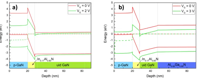
Using a 2D order to gain barrier. A sim AlGaN back-typical value Various barri shown in Fig and without t nm) and in F thickness of carriers, and depletion of enables norm expected for structure a thr The AlGaN conduction ba GaN channel However, the population in Figure 1. Si The simul gate region u equilibrium c compared to achievable. d voltage incr akage current b D self-consiste insight into t mplified struct -barrier was u es in the litera er layer thickn g. 1 and Fig. 2 the AlGaN ba Fig. 1(b) for 8 nm. Fermi separate low the channel u mally-off oper the varying reshold voltag N back-barrie and above the , electrons are e steep slope n the channel.
imulated energy
ated band dia under applied conditions and the standard reases to +2 V by five orders 2. D ent Poisson-S he achievable ture consistin sed in the sim ature. Uniform nesses and Al 2. The conduc ack-barrier are three differe carrier statis field mobility under the gate ration. Accord barrier thickn ge in the range er acts in a s e Fermi level e better confin e of the cond y band structure agrams of the gate voltage d begins to fo structure for
V with the add s of magnitude DESIGN OF Schrödinger so e threshold vo g of a 20 nm mulations. A 2D m doping wit lGaN back-bar ction band dia e given in Fig ent AlxGa1-xN stics, concentr y models for e region in th ding to the s nesses for the e of 1-2.3 V is similar manne to deplete the ned in the 2DE duction band
e for the structu
e p-GaN/InAlN are shown in orm when a ga the structure dition of the A e. F DEVICE A olver (Silvaco oltages and un p-GaN layer, DEG sheet ca th a density rrier Al-conce agrams for the . 1(a) for thre N back-barrier ration depend electron and h he absence of imulation res e p-GaN/InAlN s expected for er and in the e 2DEG. Due EG region, th caused by A ure a) without an N/GaN structu n Figure 2. D ate bias is app e with the AlG
AlGaN back-ba AND EPITA Atlas)18, the nderstand the p , In0.17Al0.83N arrier density o of 3.0×10¹⁷ c entrations wer e p-GaN/InAl ee different In r concentratio dent recombin holes were us a gate bias th sults, a thresh N/GaN struct r the varying A enhancemen to the conduc hereby leading Al-content in nd b) with AlG ures without Due to the p-G plied. The 2D GaN back-ba arrier. The Al AXY energy band d physical mech barrier layer, of 2×1013 cm -cm-3 was assu re tested. The lN/GaN struct nAlN barrier th ons (x = 0.05 nation models sed. The use o
hrough raisin hold voltage i ture. For the Al content of t nt of the p-Ga
ction band not g to the suppre the buffer le
GaN back-barrie
and with the GaN layer, th DEG begins to arrier, thus a h GaN back-bar diagrams wer hanism of the , GaN channe -2 was assumed umed for the obtained band ture in the ga hicknesses (6 5, 0.10, 0.15) s, direct trans of a p-GaN g ng the conduc in the range p-GaN/InAlN the AlGaN ba aN gate, furth tch at the inte ession of the b eads to decre
er in the gate reg
AlGaN back he 2DEG is d o form at high higher thresh rrier supresses re simulated in AlGaN back el layer and an d according to p-GaN layer d diagrams are te region with nm, 8 nm, 10 for a barrier sition of three ate causes the tion band and of 0.5-2 V is N/GaN/AlGaN ack-barrier.
her lifting the erface with the buffer current eased electron
gion.
-barrier in the depleted under her gate biases old voltage is s n -n o r. e h 0 r e e d s N e e t. n e r s s
Proc. of SPIE Vol. 10918 109181A-2
Downloaded From: https://www.spiedigitallibrary.org/conference-proceedings-of-spie on 30 Jan 2020 Terms of Use: https://www.spiedigitallibrary.org/terms-of-use
Figure 2. Si without and b) The epitax structures (Fi structures beg resistive GaN a high resistiv barrier in the was complete Using XRD f of the Mg acc Figure 4 sh fabrication w reactive ion e 30 s at 875°C gate electrode imulated band with AlGaN ba xial structures igure 3) were gin with a 30 N buffer, and a ve GaN layer e second struc ed with 20 nm fitting, the ind ceptors, the w Figure 3 hows a cross s was to pattern a etching (ICP-R C under N2 am es and subseq structure in the ack-barrier. 3. DEV s used in the f e grown on 10 00 nm AlN nu a 130 nm high before the Ga cture. A 1-2 n m Mg-doped G dium content o
afers were ann
3. a) p-GaN/InA
section view, m and dry etch t RIE). Ohmic c mbient. Mesa i quently Ti/Au e gate region un VICE STRUC fabrication of 00 mm (111) ucleation laye h mobility cha aN channel, w nm AlN space GaN capping of the InAlN l nealed in an N AlN/GaN and b micrograph an the p-GaN lay contact was m solation was p u contact pads nder equilibrium CTURE AN f the devices a silicon wafe er, followed b annel GaN gro which is replac er was grown layer with th ayer extracted N2+Air mixtur ) p-GaN/InAlN nd SEM imag yer in the drai metallization w performed usi s were deposit m (red) and ga ND FABRIC are shown in r with resistiv by AlGaN stra own at 350 m ced with a 120 prior to the 8 he hole concen d from was fo re at 830°C fo N/GaN/AlGaN e ge of the fabric n and source was done usin ing BCl3/Cl2 g ted with e-bea
te bias (green)
CATION
Figure 3. Tw vity higher th ain managing mbar. The first 00 nm low Al 8 nm InAlN b ntration of ap und to be 0.17 or 15 minutes. epitaxial structu cated devices. regions with i ng Ti/Al/Ni/A gas mixture in am evaporatio conditions for wo E-mode ep han 10 kΩ·cm layer stack, epitaxial stru content Al0.06 barrier and ep pproximately 3 7. Finally, for ures studied.
. The first step inductively-co Au. Annealling
n an ICP-RIE s on. The p-GaN
the structure a itaxial HEMT m. The HEMT 1100 nm high ucture contains 6Ga0.94N back itaxial growth 3.0×1017 cm-3 r the activation p of the device oupled plasma g was done for system. Ni/Au N layer in the a) T T h s -h 3. n e a r u e
Proc. of SPIE Vol. 10918 109181A-3
Downloaded From: https://www.spiedigitallibrary.org/conference-proceedings-of-spie on 30 Jan 2020 Terms of Use: https://www.spiedigitallibrary.org/terms-of-use
access region selectivity be fabrication w (PECVD) for LSG, and the g Figure 4. 4.1 Electrica DC charac shows the tra an AlGaN ba the p-GaN wa present for n passivation. T in the case be the conductio and only the b in Fig. 5(b). W voltages for t respectively, leakage curre located at the ns was then et etween 6 and was completed r surface passi gate-to-drain, . a) Cross sectio al Characteriz cterization wa ansfer characte ack-barrier lay as etched, and negative gate b This leakage c efore the acce on at the surfa buffer leakag With the p-Ga the devices w using the ext ent is present e intersection o tched away u 13.5, was ach d with the d ivation. The g LDG, spacings onal representat zation s carried out eristics as a fu yer. Measurem d after SiN dep biases. This c current is attri ess region p-G ace is suppress e remains. Th aN etch and S with and witho trapolation of for negative g of the extrapo using ICP-RIE hieved using B eposition of gate length, LG s are 1.75 μm.
tion of the mea
4. RESULT
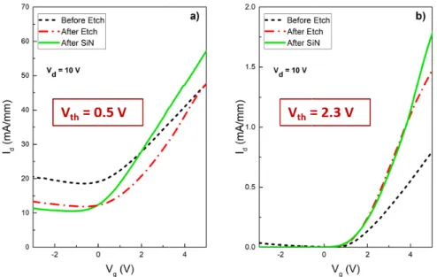
using a Keysi unction of gat ments were tak
position. In Fi current decrea ibuted to buffe GaN is etched.
sed; with the his remaining iN passivation out an AlGaN f the current a gate biases, in lated leakage E in 5-nm incr BCl3 gas at a 200 nm SiN G, is 1.5 µm, a . sured devices, b devices. TS AND DIS ight B1500A e bias at a dra ken before th ig. 5(a), it can ases after the fer leakage, su With the etch SiN passivati leakage curre n, the transcon N back-barrier
at the maximu n the bias ran
current and th
rements. Sele an ICP power N using plasm and the gate w
b) optical micro SCUSSION Semiconduct ain bias of Vd he p-GaN laye n be seen that a p-GaN in th urface defects, hing of the p-on, the leakag ent is suppress
nductance of after SiN pas um linear slop nge where the he linear extra ective etch of of 100 W an ma enhanced width, WG, is 1 ograph and c) S
tor Device Par = 10 V for th er in the acces a significant a he access regi , and conducti -GaN in the ac ge from the su sed by the AlG
the devices al ssivation are o pe. In the cas
transistor is apolation of th p-GaN over nd RF power chemical vap 100 µm. The s SEM image of th rameter Analy he devices wit ss regions wa amount of leak ion is etched
ion from the p ccess regions, urface defects GaN back-bar lso increases. obtained as 0 se of Fig. 5(a) accepted to b he Id-Vg curve InAlN, with a 30 W. Device por deposition source-to-gate he fabricated yzer. Figure 5 thout and with s etched, after kage current is and after SiN p-GaN surface , leakage from s is suppressed rrier, as shown The threshold .5 V and 2 V ), where large be “off”, Vth is . a e n e, 5 h r s N e m d n d V, e s
Proc. of SPIE Vol. 10918 109181A-4
Downloaded From: https://www.spiedigitallibrary.org/conference-proceedings-of-spie on 30 Jan 2020 Terms of Use: https://www.spiedigitallibrary.org/terms-of-use
Figure 5. M The output transfer chara SiN passivati Vg = 5 V for barrier, a drai the standard d and lower dr threshold vol show signs of in Fig. 6(b) d Figure 6. M Measured transfe t characteristi acteristic mea ion. An increa r the SiN pass in current of 2 device. The A rain current d tage and main f buffer leaka emonstrates th Measured output er characteristic cs of the fabr surements, th ase in the drain sivated device
2.2 mA/mm a AlGaN back-ba
density. The d nly the lower
ge. The upwa hat the AlGaN
t characteristics cs of the p-GaN ricated device he devices wer n current was e without the at Vg = 5 V w arrier leads to decreased cur sheet charge ard slope in th N back-barrier of the p-GaN/I N/InAlN/GaN H es on the two re measured b observed at e back-barrier. was obtained, c o a lower sheet rrent in the d density. In th he drain curren r is effective in InAlN/GaN HE HEMT a) withou heterostructur before the p-G each step. A d For the SiN p corresponding t carrier densi device with th he standard de nt seen in Figu n mitigating th EMT a) without ut and b) with a
res are shown GaN etch, afte drain current o passivated dev g to an order o
ity and therefo he back-barrie evice, Fig. 6(a
ure 6(a) and th he buffer leak t and b) with an an AlGaN back-n iback-n Fig. 6. Si er the p-GaN e of 30 mA/mm
vice with the of magnitude ore higher thre er is a result a), the output
he suppression kage current.
n AlGaN back-b -barrier.
imilarly to the etch, and after m is obtained a AlGaN back decrease from eshold voltage of the higher characteristics n of this slope barrier. e r at -m e r s e
Proc. of SPIE Vol. 10918 109181A-5
Downloaded From: https://www.spiedigitallibrary.org/conference-proceedings-of-spie on 30 Jan 2020 Terms of Use: https://www.spiedigitallibrary.org/terms-of-use
The presented HEMTs in their current state show poor performance in terms of driving current and off-state leakage performance. This may evoke a false notion that p-GaN concept is inappropriate for InAlN/GaN-based devices, however, the reason for the poor performance is unoptimized epitaxy and processing. The obtained drain current density is lower than what can be achieved with the InAlN/GaN19-21, owing to the trade-off in the annealing temperature for Ti/Al/Ni/Au Ohmic contacts between achieving low contact resistance and the degradation of the channels sheet resistance22. For Ti/Al/Ni/Au Ohmic contact metallization, the Ohmic contact resistance has been shown to decrease while carrier mobility has been shown to be stable up to annealing temperatures of 850°C, after which a significant degradation of the mobility accompanied by a decrease in sheet carrier density begins to occur22. The off-state leakage is due to poor buffer design in the epitaxy.
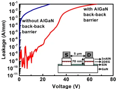
4.2 Leakage Characterization
Figure 7. Leakage test structure (inset) and leakage plot.
The leakages of the SiN passivated devices were characterized using leakage test structures (Fig. 7 inset). The test structures consist of source-drain metallization separated by 5 µm with the channel removed in the mesa isolation step. The structure without an AlGaN back-barrier demonstrates leakage starting from the order of mA/mm for the measured voltage range, whereas the structure with an AlGaN back-barrier demonstrates leakage on the order of uA/mm up to 15 V and less than 1 mA/mm up to 35 V. For typical operation voltages of a transistor, an improvement of 5 to 6 orders magnitude in leakage is observed for structures utilizing an AlGaN back-barrier over devices without a back-barrier.
5. CONCLUSION
In summary, we have demonstrated normally-off p-GaN gate HEMTs based on the InAlN/GaN heterostructure and studied the effect of AlGaN back-barriers on the DC characteristics of the said device. A positive threshold voltage of +0.5 V is achieved with the p-GaN/InAlN/GaN structure which further increases to +2 V with the use of an AlGaN back-barrier. In addition, AlGaN back-barrier devices show improved buffer leakage currents by five orders of magnitude. The reduction in drain current observed for structures with AlGaN back-barrier can be compensated by means of introducing an AlN spacer layer between the barrier layer and GaN channel or increasing the Al content of the barrier layer.
ACKNOWLEDGEMENTS
This work is supported by the TUBITAK under Project No. 116F041. One of the authors (E.O.) also acknowledges partial support from the Turkish Academy of Sciences.
Proc. of SPIE Vol. 10918 109181A-6
Downloaded From: https://www.spiedigitallibrary.org/conference-proceedings-of-spie on 30 Jan 2020 Terms of Use: https://www.spiedigitallibrary.org/terms-of-use
REFERENCES
[1] U. K. Mishra, P. Parikh, and Y.-F. Wu, "AlGaN/GaN HEMTs-an overview of device operation and applications," P IEEE 90(6), 1022-1031 (2002).
[2] K. J. Chen et al., "GaN-on-Si power technology: Devices and applications," IEEE T ELECTRON DEV 64(3), 779-795 (2017). [3] J. W. Chung, W. E. Hoke, E. M. Chumbes, and T. Palacios, "AlGaN/GaN HEMT With 300-GHz fmax," IEEE ELECTR DEVICE
L 31(3), 195-197 (2010).
[4] W. Xing et al., "InAlN/GaN HEMTs on Si With High fT of 250 GHz," IEEE ELECTR DEVICE L 39(1), 75-78 (2018).
[5] G. Dutta, S. Turuvekere, N. Karumuri, N. DasGupta, and A. DasGupta, "Positive shift in threshold voltage for reactive-ion-sputtered Al2O3/AlInN/GaN MIS-HEMT," IEEE ELECTR DEVICE L 35(11), 1085-1087 (2014).
[6] K. Jeganathan, M. Shimizu, H. Okumura, Y. Yano, and N. Akutsu, "Lattice-matched InAlN/GaN two-dimensional electron gas with high mobility and sheet carrier density by plasma-assisted molecular beam epitaxy," J CRYST GROWTH 304(2), 342-345 (2007).
[7] J. Kuzmík, "Power electronics on InAlN/(In) GaN: Prospect for a record performance," IEEE ELECTR DEVICE L 22(11), 510-512 (2001).
[8] D. S. Lee, X. Gao, S. Guo, D. Kopp, P. Fay, and T. Palacios, "300-GHz InAlN/GaN HEMTs with InGaN back barrier," IEEE ELECTR DEVICE L 32(11), 1525-1527 (2011).
[9] W. Saito, Y. Takada, M. Kuraguchi, K. Tsuda, and I. Omura, "Recessed-gate structure approach toward normally off high-voltage AlGaN/GaN HEMT for power electronics applications," IEEE T ELECTRON DEV 53(2), 356-362 (2006).
[10] Y. Cai, Y. Zhou, K. J. Chen, and K. M. Lau, "High-performance enhancement-mode AlGaN/GaN HEMTs using fluoride-based plasma treatment," IEEE ELECTR DEVICE L 26(7), 435-437 (2005).
[11] Y. Uemoto et al., "Gate injection transistor (GIT)—A normally-off AlGaN/GaN power transistor using conductivity modulation," IEEE T ELECTRON DEV 54(12), 3393-3399 (2007).
[12] T. Hashizume et al., "Al2O3 insulated-gate structure for AlGaN/GaN heterostructure field effect transistors having thin AlGaN barrier layers," JPN J APPL PHYS 43(6B), L777 (2004).
[13] G. Greco, F. Iucolano, and F. Roccaforte, "Review of technology for normally-off HEMTs with p-GaN gate," MAT SCI SEMICON PROC (2017).
[14] Z. Zaidi et al., "Enhancement mode operation in AlInN/GaN (MIS) HEMTs on Si substrates using a fluorine implant," SEMICOND SCI TECH 30(10), 105007 (2015).
[15] D. Morgan et al., "Enhancement-mode insulating-gate AlInN/AlN/GaN heterostructure field-effect transistors with threshold voltage in excess of +1.5 V," APPL PHYS EXPRESS 4(11), 114101 (2011).
[16] C. Ostermaier et al., "Ultrathin InAlN/AlN barrier HEMT with high performance in normally off operation," IEEE ELECTR DEVICE L 30(10), 1030-1032 (2009).
[17] O. Kelekci, P. Tasli, S. Cetin, M. Kasap, S. Ozcelik, and E. Ozbay, "Investigation of AlInN HEMT structures with different AlGaN buffer layers grown on sapphire substrates by MOCVD," CURR APPL PHYS 12(6), 1600-1605 (2012).
[18] ATLAS User’s Manual, Device Simulation Software, SILVACO Int., Santa Clara, CA, 2015.
[19] Y. Yue et al., "InAlN/AlN/GaN HEMTs with regrown ohmic contacts and fT of 370 GHz," IEEE ELECTR DEVICE L
33(7), 988-990 (2012).
[20] R. Wang et al., "Gate-recessed enhancement-mode InAlN/AlN/GaN HEMTs with 1.9-A/mm drain current density and 800-mS/mm transconductance," IEEE ELECTR DEVICE L 31(12), 1383-1385 (2010).
[21] H. Wang, J. W. Chung, X. Gao, S. Guo, and T. Palacios, "Al2O3 passivated InAlN/GaN HEMTs on SiC substrate with
record current density and transconductance," PHYS STATUS SOLIDI C 7(10), 2440-2444 (2010).
[22] C.-F. Lo et al., "Annealing temperature dependence of Ohmic contact resistance and morphology on InAlN/GaN high electron mobility transistor structures," J VAC SCI TECHNOL B 29(2), 021002 (2011).
Proc. of SPIE Vol. 10918 109181A-7
Downloaded From: https://www.spiedigitallibrary.org/conference-proceedings-of-spie on 30 Jan 2020 Terms of Use: https://www.spiedigitallibrary.org/terms-of-use