CMOS Realization of a
Quantized-Output Classifier Circuit
Merih YıldızDepartment of Electronics and Communications Engineering, Dogus University, Acibadem,
Kadikoy 34722, Istanbul [email protected]
Shahram Minaei Department of Electronics and Communications Engineering, Dogus University, Acibadem,
Kadikoy 34722, Istanbul. [email protected]
İzzet Cem Göknar Department of Electronics and Communications Engineering, Dogus University, Acibadem, Kadikoy 34722, Istanbul. [email protected]
Abstract— In this paper a CMOS implementation of a multi-input data classifier with several output levels and a different architecture is presented. The proposed circuit operates in current-mode and can classify several types of analog vector data. The classifier circuit’s new architecture consists of the interconnections of core cells each possessing a current-voltage converter, an inverter followed by a NOR gate and a voltage-current output stage. Using 0.35µm TSMC
technology parameters, SPICE simulation results for a classifier with two inputs are included to verify the expected results.
I. INTRODUCTION
The aim of classification is to assign an unknown object to a class containing similar objects. Classifier circuits can find applications in various fields of applied science such as automatic target recognition, real-time object recognition, pattern recognition, artificial intelligence, neural networks and statistics [1-5].
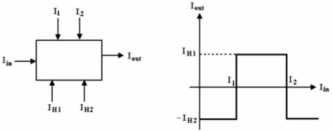
In this paper a one-dimensional classifier, called core circuit, shown in Fig. 1a with transfer characteristic as in Fig. 1b is used to realize an n-dimensional classifier as shown in Fig. 2 with an architecture resembling that of a 1-layer neural network. The current Iin is the 1-dimensional
data for each core circuit and Iout is the output of the
classifier; it should be observed that by grouping core circuits and adding the outputs in each group a multi-output classifier can be obtained as well. The transfer characteristic of the block in Fig. 1b is similar to a Trapezoidal Activation Function (TAF) [6] which is used in PWL approximation, high-speed folding analog-to-digital converters, fuzzy controllers, etc. The stability properties of neural networks with TAF have been investigated in [7] and a switched capacitor CMOS implementation of a cell with TAF has been proposed in [8]. Neurons with double threshold activation function have been investigated in literature and used to classify data separable by two parallel hyperplanes [9]. The primary aim of this paper is to develop a classifier circuit with n inputs and externally tunable decision regions and different amplitude in each region. In order to achieve this, an analog CMOS current-mode realization of a one-dimensional “classifier” circuit (core neuron) is realized. One-dimensional classifier can be used as a quantizer which in turn can be used for analog digital conversion.
Figure 1.a. Core circuit block diagram. Figure 1.b. Transfer characteristic of the core circuit.
Figure 2. Block diagram of an n-dimensional classifier.
The classifier circuit has been simulated: i) with one input to illustrate the effects of quantization and ii) with two inputs to show the result of two-dimensional multilevel classification. As mentioned before the core neuron of the proposed circuit has a dc transfer characteristic as depicted in Fig. 1.b. The horizontal position, the width and the height of the transfer characteristic can be adjusted independently by means of external currents I1, I2 and IH1 and IH2. Using
several core circuits as shown in Fig. 2, a multi-dimensional, multi-level-output (each level corresponding to the coding of a data class) classifier is obtained.
Figure 3. Block diagram of the core circuit.
II. CMOSREALIZATION OF THE CORE CIRCUIT
The input-output transfer characteristic shown in Fig. 1.b can be expressed as:
− < < = II for I otherwiseI I I 2 H 2 in 1 1 H out (1) The currents IH1 and IH2 as shown in Fig. 1.b are the
positive and negative heights of the output current. The currents I1 and I2 are used to shift the horizontal position and
adjust the width of the output current.
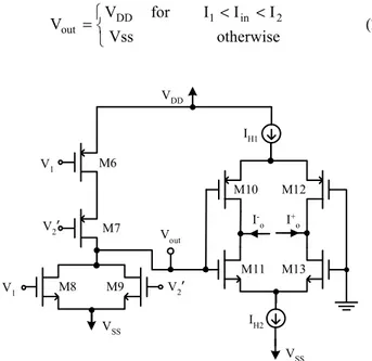
The proposed block diagram for realizing the core circuit with transfer characteristic of Fig. 1.b is shown in Fig. 3. It consists of a current-to-voltage input stage with two different outputs V1 and V2, an inverter, a NOR gate and a
voltage-to-current output stage. The input stage and the inverter of the core circuit are shown in Fig. 4.
Figure 4. The input stage of the core circuit with the inverter.
The diode-connected transistor M1 and the bias current
IBIAS form a current-to-voltage converter. The transistors M2
and M3 are biased with different currents IBIAS+I1 and
IBIAS+I2 to form two different threshold currents of the
transfer characteristic. The transistors M1, M2 and M3 are
matched. The transistors M4 and M5 constitute an inverter
which is used to obtain an input-output characteristic with negative jump at threshold current I2.
The NOR gate and the output stage of the proposed core circuit are shown in Fig. 5. The desired nonzero part of the
transfer characteristics is obtained by the NOR gate (transistors M6, M7, M8 and M9) as follows: if both inputs of
the NOR gate are at low level then the output of the gate is at high level, otherwise at low level. In fact Vout can be written
as: < < = otherwise Vss I I I for V Vout DD 1 in 2 (2) IH2 M7 M6 M8 M9 M10 M11 M12 M13 I+ o VDD V1 V1 V2’ Vout V2’
.
.
.
I -o VSS VSS IH1Figure 5. The NOR gate and the output stage of the core circuit.
The location of the nonzero portion of the output is fixed with the currents I1 and I2. This shift of the intercept points
by adjusting the starting and ending boundary points of the specified decision region makes the device custom tunable. The currents IH1 and IH2 determine the peak values of the
function. The current output stage of the circuit is obtained by connecting two complementary source-coupled pairs [10].
The current relations are IDM10+I−o=IDM11,
IDM12+I+o=IDM13, IH1=IDM10+IDM12 and IH2=IDM11+IDM13.
The output currents + o I and −
o
I can be given in terms of Vout as follows: = − = = + SS out 2 H DD out 1 H o I for V V V V for I I (3) 293
= = − = − SS out 1 H DD out 2 H o I for V V V V for I I (4)
It should be noted that in the next section the current I+o is used as the output current Iout, the current IH2 is chosen as
0 and the current IH1 denoted by IH is used to change the
height of the transfer characteristic.
III. SIMULATION OF THE MULTILEVEL CLASSIFIER
CIRCUIT
To classify different types of data the proposed core circuits’ outputs can be connected “in parallel” as shown in Fig. 2. In order to achieve the 1-D input-output characteristic shown in Fig. 6 the following constraints must be satisfied:
in inn 2 in 1 in I ... I I I = = = = (5) n 2 ) 1 n 2 ( 3 2 1 I I ... I I I < < < < − < (6)
Figure 6. Desired Input-Output characteristic for the classifier.
Also the block diagram for realizing a 2-D multilevel classifier with two different input currents (Iin1, Iin2) is shown
in Fig. 7.
The proposed core circuit is simulated using SPICE with 0.35µm TSMC MOSIS CMOS technology parameters. The voltage supply used in the proposed circuit is ±1.25 V, the current IBIAS is chosen as 0.1µA. The dimensions of the
transistors are given in Table I.
The control currents and the power dissipation for the 2-D multilevel classifier block diagram of Fig. 7 are shown in Table II. The current Iin1 is applied to core circuit-1 and core
circuit-2, and the current Iin2 is applied to core circuit-3 and
core circuit-4.
SPICE simulation results for two different inputs to the classifier circuit are shown in Fig. 8. It can be seen from Fig. 8 that there are 8 different regions. So this kind of configuration can classify two-dimensional data into 8 different types of classes (9 if counting the Iin1-Iin2 plane)
each type being encoded with a different output current value.
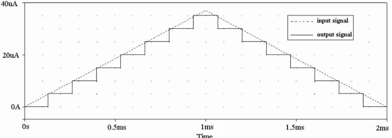
To construct a quantizer circuit with eight quanta, eight core circuits need to be connected in parallel with the same
input currents (Iin) and eight different sets of control
currents. The selected classification parameters I1, I2 and the
resolution parameter IH for each core circuit are given in
Table III.
To simulate the circuit as a quantizer a single triangular input waveform is applied to the input of the circuit and the input-output characteristic versus time is shown in Fig. 9. It should be observed that quanta width and peak value can be tuned at will thus providing further design flexibility.
TABLEI.
DIMENSIONS OF THE MOS TRANSISTORS
MOSFET M1, M2, M3, M4, M6,
M7, M8, M9,M10, M11 M5 M12, M13
W [µm] 10 5 16
L [µm] 0.7 0.7 0.7
TABLEII.
CORE CIRCUIT PARAMETERS (CURRENTS IN µA)
Core Circuit-I Power
Dissipation
Core Circuit-II Power
Dissipation
I1 I2 IH1 I3 I4 IH2
70 140 60 0.35mW 210 280 120 0.77mW
Core Circuit-III Power
Dissipation
Core Circuit-IV Power
Dissipation
I5 I6 IH3 I7 I8 IH4
60 140 100 0.39mW 280 360 80 0.91mW
TABLEIII
CORE CIRCUIT (CC)PARAMETERS USED IN QUANTIZER CIRCUIT
CC1 CC2 CC3 CC4 CC5 CC6 CC7 CC8
I1 (µA) 0 5 10 15 20 25 30 35
I2 (µA) 40 40 40 40 40 40 40 40
IH (µA) 0.1 5 5 5 5 5 5 5
IV. CONCLUSION
In this paper, a current mode CMOS-only core circuit has been introduced and using this core circuit, a very flexible neural network like architecture has been designed and its abilities demonstrated. This circuit possessing a transfer characteristic with independently tunable heights, width and horizontal position, the proposed architecture can be used for a variety of purposes such as classification, quantization etc. Another advantage of the proposed circuit is its ability to operate at low supply voltages. Because of the parallel processing characteristic of the circuit, it is well-suited for real-world applications.
Figure 7. Block diagram of a two-dimensional multilevel classifier circuit.
Figure 8. (Iin1-Iin2)-Iout characteristic of the proposed two-dimensional multilevel classifier.
Figure 9. Iin-Iout characteristic of the eight level quantizer circuit.
REFERENCES
[1] B. Liu, C. Chen, and J. Tsao, “A Modular Current-Mode Classifier Circuit for Template Matching Application”, IEEE Trans. on Circuit and Systems-II, Analog and Digital Sig. Process. vol. 47, No. 2, pp. 145-151, 2000.
[2] E. Hunt , Artificial Intelligence. New York : Academic, 1975.
[3] H.S. Abdel-Aty-Zohdy, M. Al-Nsour, “Reinforcement learning neural network circuits for electronic nose” IEEE International Symposium on Circuits and Systems, Orlando, FL, vol. 5, 30 May-2 June, 1999, pp. 379 – 382.
[4] G. Lin and B. Shi, “A current-mode sorting circuit for pattern recognition” Intelligent Processing and Manufacturing of Materials, Honolulu, Hawaii, July 10-15, 1999, pp. 1003 – 1007.
[5] G. Lin and B. Shi, “A multi-input current-mode fuzzy integrated circuit for pattern Recognition” Second International Conference on Intelligent Processing and Manufacturing Materials, Honolulu, Hawaii, July 10-15, 1999, pp. 687-693.
[6] M. Kachare, J. Ramirez-Angulo, R. Carvajel, and A. J. Lopez-Martin, “New Low-Voltage Fully Programmable CMOS Triangular/Trapezoidal Fucntion Generator Circuits”, IEEE Trans. on Circuit and Systems-I, Vol. 52, No. 10, pp. 2033-2040, Oct. 2005.
[7] E. Bilgili, İ.C. Göknar and O.N. Uçan, "Cellular Neural Networks with Trapezoidal Activation Function," Int. Journal of Circuit Theory and Applications, Vol. 33, No. 5, pp. 393-417,2005.
[8] D.Y. Aksın, S. Aras, İ.C. Göknar, "CMOS Realization of User Programmable, Single-Level, Double-Threshold Generalized Perceptron," Proceedings of Turkish Artificial Intelligence and Neural Networks Conference, İzmir, Turkey, June 21-23, 2000.
[9] M. Yıldız, S. Minaei, C. Göknar, “Current Mode Double Threshold Neuron Activation Function”, Complex Computing-Networks: Brain-like
and Wave-oriented Electrodynamic Algorithms. Springer Proceedings in
Physics, Netherlands: Springer, 2006, pp. 267-274
[10] A. F. Arbel and L. Goldminz, “ Output Stage for Current-Mode Feedback Amplifier, Theory and Applications”, Analog Integrated Circuits and Signal Processing vol. 2 issue. 3 , pp. 243-255, 1992.