a thesis
submitted to the department of computer engineering
and the institute of engineering and science
of bilkent university
in partial fulfillment of the requirements
for the degree of
master of science
By
Dilek Demirba¸s
July, 2011
Asst. Prof. Dr. ¨Ozcan ¨Ozt¨urk (Advisor)
I certify that I have read this thesis and that in my opinion it is fully adequate, in scope and in quality, as a thesis for the degree of Master of Science.
Assoc. Prof. Dr. U˘gur G¨ud¨ukbay
I certify that I have read this thesis and that in my opinion it is fully adequate, in scope and in quality, as a thesis for the degree of Master of Science.
Asst. Prof. Dr. Defne Akta¸s
Approved for the Institute of Engineering and Science:
Prof. Dr. Levent Onural Director of the Institute
NETWORK-ON-CHIP DESIGN
Dilek Demirba¸sM.S. in Computer Engineering Supervisor: Asst. Prof. Dr. ¨Ozcan ¨Ozt¨urk
July, 2011
With increasing communication demands of processors and memory cores in Systems-on-Chips (SoCs), application-specific and scalable Network-on-Chips (NoCs) are emerged to interconnect processing cores and subsystems in Multi-processor System-on-Chips (MPSoCs). The challenge of application-specific NoC design is to find the right balance among different trade-offs such as communica-tion latency, power consumpcommunica-tion, and chip area.
This thesis introduces a novel heterogeneous NoC design approach where bi-ologically inspired evolutionary algorithm and 2-dimensional rectangle packing algorithm are used to place the processing elements with various properties into a constrained NoC area according to the tasks generated by Task Graph for Free (TGFF). TGFF is one of the pseudo-random task graph generators used for scheduling and allocation. Based on a given task graph, we minimize the maximum execution time in a Heterogeneous Chip-Multiprocessor. We specifi-cally emphasize on the communication cost as it is a big overhead in a multi-core architecture. Experimental results show that our approach improves total com-munication latency up to 27% with modest power consumption.
Keywords: Network-on-Chip (NoC) synthesis, Multiprocessor-System-on-Chip (MPSoC) design, Heterogeneous Chip-Multiprocessors.
M˙IKRODEVRE A ˘
G TASARIMI
Dilek Demirba¸sBilgisayar M¨uhendisli˘gi, Y¨uksek Lisans Tez Y¨oneticisi: Asst. Prof. Dr. ¨Ozcan ¨Ozt¨urk
Temmuz, 2011
˙I¸slemci ve bellek ¸cekirde˘gi arasındaki artan haberle¸sme ihtiyacından ¨ot¨ur¨u, C¸ ok ˙I¸slemcili Mikrodevre Sistemler (C˙IMS)’deki i¸slemci ¸cekirdekleri ve alt dizgeleri ba˘glamak i¸cin, uygulamaya ¨ozg¨u ve ¨ol¸ceklenebilir Mikrodevre A˘glar (MA) ortaya ¸cıktı. Uygulamaya ¨ozg¨u mikrodevre tasarımların zorlu˘gu, haberle¸smeden kaynaklı gecikme, g¨u¸c t¨uketimi ve mikrodevre alanı gibi farklı ¨
od¨unle¸simler arasındaki do˘gru dengeyi bulmaktır.
Bu tez, farklı ¨ozelliklere sahip i¸slemci ¸cekirdeklerini, Serbest Kullanılabilir ˙I¸s Y¨uk¨u Grafi˘gi (SKIYG)’nden ¨uretilen i¸s y¨uklerine g¨ore, belirlenen mikrode-vre a˘g alanına yerle¸stirmek i¸cin, dirimbirimsel ilhamlı evrimsel ¸c¨oz¨um yolu ve 2 boyutlu ¸c¨oz¨um yolunun kullanıldı˘gı, yeni bir mikrodevre a˘g tasarım yakla¸sımını tanıtıyor. SKIYG, zaman ¸cizelgelemesi ve b¨ol¨u¸st¨urmede kullanılan, rastgele i¸s y¨uk¨u ¨ureten ara¸clardan bir tanesidir. Verilen i¸s y¨uk¨u ¸cizelgesine g¨ore, t¨urde¸s olmayan ¸cok i¸slemcili mikrodevredeki azami haberle¸sme maliyetini en aza in-dirgiyoruz. ¨Ozellikle haberle¸sme maliyeti ¨uzerine yo˘gunla¸smamızın nedeni, ¸cok i¸slemcili bir mimaride haberle¸sme maliyetinin ¨onemli bir gider olmasıdır. Deney-sel sonu¸clar, bizim yakla¸sımımızın, kabul edilebilir bir g¨u¸c t¨uketimiyle birlikte toplam haberle¸sme gecikmesini %27’lere kadar indirgedi˘gini g¨osteriyor.
Anahtar s¨ozc¨ukler : Mikrodevre A˘g (MA) sentezi, C¸ ok ˙I¸slemcili Mikrodevre Sis-tem (C¸ ˙IMS) tasarımı, t¨urde¸s olmayan ¸cok i¸slemcili mikrodevre.
I would like to thank my supervisor, Asst. Prof. Dr. ¨Ozcan ¨Ozt¨urk for always being available when I needed help. He has always supported and motivated me, and provided valuable feedback to reach my goals.
I also thank to Assoc. Prof. Dr. U˘gur G¨ud¨ukbay for his valuable comments and help throughout this study.
I am grateful to my jury member, Asst. Prof. Dr. Defne Akta¸s for reading and reviewing this thesis.
Last but not the least, I thank to my family for supporting me with all my decisions and for their endless love...
1 Introduction 1
1.1 Motivation . . . 1
1.2 Research Objectives . . . 4
1.3 Overview of the Thesis . . . 6
2 Related Work 7 3 Methodologies 11 3.1 Heuristic Algorithm . . . 11
3.1.1 Implementation Details of Genetic Algorithm . . . 12
3.2 2D Bin Packing . . . 20
3.2.1 Problem Formulation and Basic Approach . . . 21
3.2.2 2D Bin Packing Methodology . . . 28
4 Experimental Results 40
4.1 Experimental Results of Genetic Algorithm . . . 41
4.2 Experimental Results of 2D Bin Packing Algorithm . . . 42
4.2.1 Packing Efficiency . . . 42
4.2.2 Application-specific Latency-aware Heterogeneous NoC Design . . . 44
4.2.3 Task Scheduling Algorithm Analysis for MCNC Benchmarks 61
4.2.4 Algorithm Intrinsics . . . 63
5 Conclusion and Future Work 67
A Sample Layouts 75
A.1 TGFF-Semi Synthetic Layouts . . . 75
A.2 Minimum Dead Area Layouts . . . 80
B E3S Benchmark 82
B.1 E3S Tasks . . . 82
B.2 E3S Processors . . . 85
C Code 86
C.1 Simulated Annealing . . . 86
1.1 Different NoC topologies. . . 3
3.1 The algorithm for exploring a latency-aware NoC topology and processing core placement. . . 12
3.2 Communication latency decision step. . . 14
3.3 Initialization step of the Genetic Algorithm. . . 15
3.4 Crossover point selection. . . 17
3.5 The result of the crossover operation. . . 17
3.6 Sample task graph representing TGFF task graphs. . . 23
3.7 A task having two parents. . . 26
3.8 The overview of the proposed approach. . . 27
3.9 Scheduled task graph into heterogeneous NoC. . . 29
3.10 The algorithm for exploring an application specific and a latency-aware NoC topology. . . 30
3.11 Feasible points for the current heterogeneous NoC layout. . . 36
3.12 Various task scheduling algorithms. . . 38
4.1 Latency comparison of Genetic Algorithm with random algorithms. 42
4.2 The task graphs from the auto-indust-mocsyn benchmark. . . 46
4.3 Textual representation of the task graph 2 from the benchmark auto-indust-mocsyn. . . 47
4.4 The communication volumes in a TGFF task graph. . . 48
4.5 Sample task graph generated by TGFF. . . 49
4.6 Comparison of CompaSS and presented algorithm on MCNC benchmarks. . . 51
4.7 Performance comparison for different task graphs. . . 51
4.8 Normalized latency for E3S benchmarks. . . 53
4.9 Normalized power consumption for E3S benchmarks. . . 54
4.10 Normalized power consumption for different task scheduling schemes. 54 4.11 Normalized algorithm execution time (ms) for E3S benchmarks. . 55
4.12 Latency for larger benchmarks. . . 56
4.13 Power consumption for larger benchmarks. . . 56
4.14 Number of processing cores placed on chip area. . . 57
4.15 Latency for 1024 tasks on 256, 512 and 1024 processing cores. . . 58
4.16 Latency for 2048 tasks on 256, 512, 1024 and 2048 processing cores. 58 4.17 Power consumption of 1024 tasks in different settings. . . 59
4.18 Power consumption of 2048 tasks in different settings. . . 59
4.19 Number of processing cores packed on a given chip area for 1024 tasks. . . 60
4.20 Number of processing cores packed on a given chip area for 2048 tasks. . . 60
4.21 Compass benchmark for Minimum Execution Time Scheduling scheme. . . 61
4.22 Compass benchmark for Direct Scheduling scheme. . . 62
4.23 Compass benchmark for Random Scheduling scheme. . . 62
4.24 Overall task scheduling comparison for Compass benchmark. . . 63
4.25 Latency versus the number of iterations for the base algorithm. . 64
4.26 Latency versus the number of iterations for the simulated annealing version. . . 65
4.27 Execution time versus the number of iterations for the base algo-rithm. . . 65
4.28 Execution time versus the number of iterations for the simulated annealing version. . . 66
A.1 Sample layout containing 256 processing cores for a task graph with 2048 tasks. . . 76
A.2 Sample layout containing 512 processing cores for a task graph with 2048 tasks. . . 77
A.3 Sample layout containing 1024 processing cores for a task graph with 2048 tasks. . . 78
A.4 Sample layout containing 2048 processing cores for a task graph with 2048 tasks. . . 79
A.5 Sample layout containing 300 processing cores with dead area 2.3%. 80
3.1 The nomenclature for the communication latency calculation. . . 21
3.2 Processor types having different dimensions. . . 22
3.3 Goodness numbers used to decide the placement of the current processor. . . 37
4.1 FEKOA benchmark content. . . 43
4.2 The performance comparison of LWF with well-known packing al-gorithms. . . 43
B.1 Consumer benchmark of E3S. . . 82
B.2 Networking benchmark of E3S. . . 83
B.3 Automotive/Industrial benchmark of E3S. . . 83
B.4 Office automation benchmark of E3S. . . 84
B.5 Telecom benchmark of E3S. . . 84
B.6 E3S processor list. . . 85
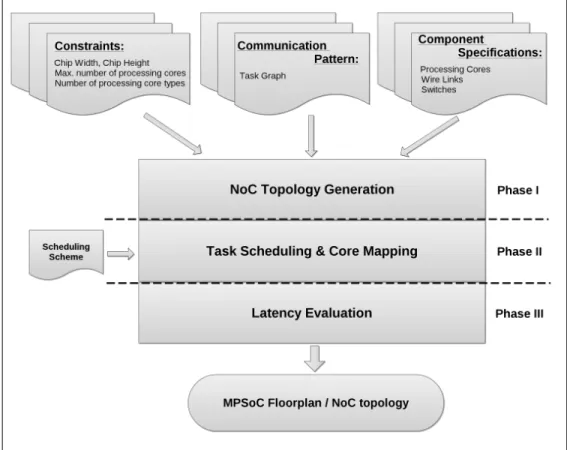
Introduction
1.1
Motivation
Advancements in production and material technology allow us to manufacture integrated circuits known as Multiprocessor System-on-Chips (MPSoCs) that contain various processing cores, along with other hardware subsystems such as memory and networking subsystems. Having different types of communicating processing cores and subsystems in MPSoCs makes it necessary to have well-designed Network-on-Chips (NoCs) to connect them. Application-independent NoCs are desired for general usage. However, for a specific usage of a NoC design which repeats the same operations, the NoC design should manipulate the tasks at top most level, where the tasks given beforehand have different loads. An application-specific NoC is needed to handle these tasks. For homogeneous NoC designs, there is no complexity for designing the layout, because each processing core is similar to each other. For a heterogeneous NoC design which contains a few processors, there is no need for an automated approach because finding the optimal layout is a practical task. However, if the number of heterogeneous processors reaches to hundreds or thousands, finding the optimum layout for the given tasks will be impractical. Therefore, a custom, application-specific het-erogeneous NoC is necessary to fulfill the requirements of a targeted application
domain within the given constraints. Such constraints include communication la-tency incurred in NoCs, total execution time of a given set of applications, power consumption and chip area. Most of the time, if not always, there are trade-offs among these constraints. It is essential to find the right balance among trade-offs to maximize resource utilization. We propose an application-specific heteroge-neous NoC design algorithm to generate a network topology and a floor-plan for NoC-based MPSoCs. Our work is complementary to task-scheduling and core-mapping efforts in MPSoCs that are considered separate phases in the design and decision processes.
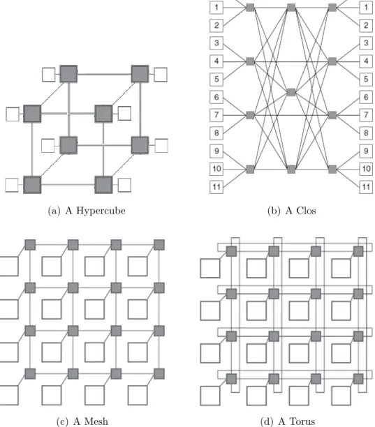
Multi-cores as well as many-cores have become mainstream in the produc-tion of Very-Large-Scale Integraproduc-tion (VLSI) circuits. Although the number of processing cores on a chip area increases, managing computation and communi-cation of these cores remains challenging. It is crucial to provide an effective and scalable communication architecture to utilize an increased number of processing cores embedded in a chip area. NoCs have been proposed and manufactured to provide a scalable communication architecture with some Quality of Service (QoS) guarantees. Many examples of NoC topologies, such as Hypercube, Clos, Butterfly, Mesh and Torus (shown in Figure 1.1 [33]), have effectively been used in System-on-Chips (SoCs) with homogeneous processing cores. However, they do not fulfill the requirements of next-generation MPSoCs that consist of hetero-geneous processing cores and other hardware components. The heterogeneity of processing cores is due to variations in size, computation and communication ca-pabilities, thus, traditional NoC topologies and tile-based floor-plans do not work for them. State of the art homogeneous NoC topologies do not distinguish cores as they share the same characteristics. However, in heterogeneous NoC design, the placement of a processor affects the overall communication latency, thereby making it a crucial design decision.
In the process of designing MPSoCs, architects and designers must decide what kind of processing cores should be used to realize the desired chip. However, the immense amount of variation in processing cores makes this decision tedious and error prone. Thus, figuring out the types of processing cores to be used in MPSoCs has a great importance. With the given objectives, our algorithm
(a) A Hypercube (b) A Clos
(c) A Mesh (d) A Torus
identifies the processing cores that can be used in MPSoCs and places them on a given chip area in a way that the total latency occurring on the chip is minimized, while the given area is utilized as much as possible. It should be noted that the regular NoC topologies are inappropriate for such cases because MPSoCs have non-uniform sets of processing cores. Thus, an effective custom NoC is the key to achieving the desired performance of an MPSoC.
1.2
Research Objectives
Application-specific NoC design is necessary to fulfill the requirements of the de-sired MPSoC with the given constraints and available budget. One important constraint is the communication latency that occurs among communicating pro-cessing cores; our focus is on an NoC design that minimizes this communication latency while still considering other constraints. In our implementation, commu-nication latency is simply defined as the total time observed among processors that are communicating due to the tasks assigned to them. We introduce an application-specific communication latency-aware heterogeneous NoC design al-gorithm that considers the given constraints and generates a floor-plan for the desired MPSoC. Our approach takes a directed and acyclic task graph, a con-strained chip area, and a set of processing core types as an input. Then it produces an application-specific heterogeneous NoC design based on the given tasks. Our heterogeneous NoC design algorithm has two objectives:
• to select appropriate processing cores from the available processor pool that will be used in heterogeneous NoC, and
• to place selected processing cores on a given chip area.
These objectives are to be attained in such a way that the total execution of the overall application is minimized.
• biologically inspired evolutionary computational approach (a Genetic Algo-rithm), and
• 2D Bin Packing.
First of all, we solve the mapping and selection problem using a Genetic Al-gorithm. In the Genetic Algorithm, there are 5 important phases. These are initialization, selection, crossover, mutation, and termination which will be ex-plained in detail in Section 3.1.1. To apply Genetic Algorithm phases, we need a population which consists of individuals. A typical NoC placement is called an individual in our implementation. A collection of individuals indicate the final selection and mapping of the processors into the given chip area. Since the ini-tialization step of the Genetic Algorithm suffers from packing procedure, we used 2D Bin Packing Algorithm to solve the same problem. In 2D Bin Packing Algo-rithm, we are given a rectangular area and a set of n rectangular items having different dimensions and these rectangles are packed into the given area without overlapping. The main objective of the 2D Bin Packing Algorithm is utilizing the given area while our main concern is minimizing the communication latency. Therefore, we converted this algorithm into our problem domain. Since the lay-out that is found by 2D Bin Packing Algorithm is prone to end up with a local optimum layout, we enhanced this algorithm by simulated annealing technique. With this modified algorithm, our goal is to reach the global optimum result. The details of the 2D Bin Packing Algorithm is given in Section 3.2. These strategies are the first ones, to our knowledge, that explore the application-specific layout which considers both the minimum communication latency and the chip area utilization.
Along with generation of custom NoC topology, there are two other impor-tant concerns that affect the overall performance of MPSoC: task scheduling and core mapping. Basically, task scheduling is to identify the processing core that will run the given task. Core mapping, on the other hand, is to place a given processing core on a given NoC. There are various studies of task scheduling and core mapping, such as A3MAP [20] and NMAP [35], in which the authors con-sider the NoC to be fixed and given beforehand. Our work is complementary to
task scheduling and core mapping because their effectiveness is tightly coupled to the NoC that is being used. Our algorithm cooperates with task-scheduling and core-mapping algorithms during the generation of the desired NoC and the floor-plan for the MPSoC. Our implementation shows that multiple constraints must be considered simultaneously, even though they belong to separate stages of the MPSoC design process.
1.3
Overview of the Thesis
The thesis is organized as follows:
• Chapter 2 gives the Related Work in the NoC and MPSoC domain.
• Chapter 3 examines the methodologies that we have used, namely Genetic Algorithm and 2D Bin Packing Algorithm.
• Chapter 4 concludes and gives the future work on voltage island based implementations.
• A set of sample layouts, the details of the benchmarks used in experimental results, and the major components of the implementation are given in the Appendix.
Related Work
MPSoCs [31, 32] has become popular due to its promising architecture combin-ing different types of processcombin-ing cores, networkcombin-ing elements, memory components and other hardware subsystems on a single chip. One of the major distinctions of MPSoC technology is its communication architecture. In distributed multi-processors, communication between the processing cores is performed through traditional networking components such as Ethernet, which although provides high bandwidth, may suffer from high latency for critical applications. On the other hand, the processing cores communicate through bus, crossbar and/or NoC technologies [21, 36, 24] in MPSoCs that provide lower latency compared to Eth-ernet. Among the communication types used in MPSoCs, NoC seems the only solution for very large scale MPSoC designs.
The main concerns in designing NOCs include power consumption, perfor-mance, area, bandwidth, latency, throughput, and wire length. Cong et al. [8] de-velop an algorithm that minimizes the dead area on the chip. Ye and Micheli [50] try to minimize the wire length of resulting NoCs. Ching et al. [7] and Lee et al. [27] minimize the power consumption by voltage island generation technique. Ching et al. [7] propose an algorithm where they try to partition a given m x n grid into a set of regions while decreasing the total number of regions as much as possible. They use a threshold which is based on the fact that the voltage assigned to a cell should not be lower than the required voltage. There
is a similar survey done by Hu et al. [18] where authors first partition the given area into a set of voltage islands and cores, followed by area-planning and floor-planning. Their objective is to simultaneously minimize power consumption and area overhead, while keeping the number of voltage islands less than or equal to a designer-specified threshold. Lee et al. [27] present an algorithm where they apply a dynamic programming based approach to assign the voltage levels. Ma and Young [30] propose an algorithm which is similar to [27]. They partition a given area into a set of voltage islands with the aim of power saving. Their floor-planner algorithm can be extended to minimize the number of level shifters between different voltage islands and to simplify the power routing step.
Kim and Kim [23] try to find a balance between the area utilization and total wire length. There exist commercial and non-commercial tools for NoC design. One of them is Versatile Place and Route (VPR) [3], which is a packing, placement and routing tool that minimizes the routing area. Kakoee et al. [22] develop another tool that is claimed to be more interactive. A survey on NoC design was conducted by Murali et al. [34] who also design an application-specific NoC with floor-plan information. Their main concern is the wiring complexity of the NoC during the topology generation procedure. Murali and Micheli [35] present a fast algorithm called NMAP for core mapping into mesh-based NoC topology while minimizing the average communication delay. For custom NoCs and irregular mesh, a core graph, which describes the communication among dif-ferent cores, is needed for floor-planning. Min-cut partitioning on the task graph is explored by Leary et al. [26], who produce a floor-planning-aware core graph. Jang and Pan [20] propose an architecture-aware analytic mapping algorithm called A3MAP for both min-cut partitioning and mapping with homogeneous cores and heterogeneous cores. Hu et al. [19] propose a method for minimizing latency and decreasing power consumption.
An Integer Linear Programming (ILP)-based approach is introduced in [42] to minimize the total energy consumption of NoCs. Banerjee et al. [2] follow a similar approach and propose a Very High Speed Integrated Circuit Hardware Descrip-tion Language (VHDL)-based cycle-accurate register transfer level model. They considered the trade-off between power and performance. Srinivasan et al. [44]
present a survey on these approaches considering performance and power require-ments. Another concern is the minimization of execution time of the placement algorithms with the help of ILP [37]. Srinivasan and Chatha [43] propose another ILP-based approach that takes throughput constraints into account.
Heterogeneous chip multiprocessor design requires the placement of different types of processors in a given chip area that resembles a 2D Bin Packing problem with additional constraints such as latency. The placement problem can be sep-arated into two: global and detailed placement. Detailed placement was studied by Pan et al. [39]. Hdjiconstaninusu and Iori [15] present a heuristic approach for solving 2D single large object placement problem, called 2SLOPP.
Hybrid genetic algorithms for the rectangular packing problem are presented by Schnenke and Vornberger [41]. They target various problems such as con-strained placement, facility layout problems and generation of VLSI macro cell layouts. Terashima-Mar´ın et al. [46] introduce a hyper-heuristic algorithm and classifier systems for solving 2D regular cutting stock problems. Pal [38] compares three heuristic algorithms for the cutting problem. He compares the performance of the algorithms based on the wasted area. In addition to heuristic algorithms, optimal rectangle placement algorithms have been proposed for certain special cases. Healy and Creavin [16] propose an algorithm that has O(N logN ) time. They try to solve the problem of placing a rectangle in a 2D space that may not have the bottom left placement property. Cui [10] studies a recursive algo-rithm for generating two-staged cutting patterns of punched strips. Lauther [25] introduces a different placement algorithm for general cell assemblies, using a combination of the polar graph representation and min-cut placement. Wong et al. [47] develop a similar algorithm that employs simulated annealing and that tries to minimize the total area and wire length simultaneously. Cong et al. [9] compare a set of rectangle packing algorithms to observe area-optimal packing. They minimized the maximum block aspect ratio subject to a zero-dead-space constraint. There are different types of packing algorithms, namely Parquet [1], B*-tree [6], TCG-S [28] and BloBB [5] that Cong et al. used to compare the area-optimality of their algorithm. We also compare our algorithm with these algorithms.
Wei et al. [48] deal with the 2D rectangular packing problem, also called the rectangular knapsack problem, which aims to maximize filling rate. They divide the problem into two stages: first they present a least-wasted strategy that evaluate the positions of rectangles, and then conduct a random local search to improve the results. The latency-aware NoC design algorithm that we present in this paper is based on their work. The details are given in Section 3.2.2.
Methodologies
3.1
Heuristic Algorithm
As a first methodology, we use a biologically-inspired evolutionary (genetic) al-gorithm, that places processing cores on a given chip area while satisfying the communication latency constraints. Genetic Algorithm is selected because it solves problems relatively in a short time and generates reasonable templates to cover all features of a problem.
Our goal is to minimize the maximum execution latency among heterogeneous CMPs on NoC by finding optimal layout within a given chip area budget in a reasonable amount of time. We propose an approach to generate NoC architec-ture that includes hundreds to thousands of heterogeneous processors by using a heuristic algorithm. By the help of Genetic Algorithm;
• We minimize the communication latency, which includes communication and computational costs. Figure 3.1 illustrates two heterogeneous NoC designs obtained using the proposed approach. In Figure 3.1 (a), a het-erogeneous NoC layout is generated with the order of P2, P1, P2, P3 and in Figure 3.1 (b), the places of the processors are changed. There are four
(a) First heterogeneous NoC layout. (b) Second heterogeneous NoC layout.
Figure 3.1: The algorithm for exploring a latency-aware NoC topology and pro-cessing core placement.
tasks and they are mapped one-to-one to the processors. Maximum commu-nication latency for the first layout is greater than the second heterogeneous NoC layout. Therefore, we select the second layout. We aim to minimize the maximum latencies by remapping processors on chip without changing tasks.
• We reduce the execution time significantly.
• The proposed approach provides an infrastructure for multi-functional de-vices [45].
3.1.1
Implementation Details of Genetic Algorithm
The Genetic Algorithm is a search technique that is used to find optimal or approximate solutions to the given problem set. It is a kind of evolutionary algo-rithm that is inspired from crossover of chromosomes. It uses the initialization, mutation, selection and crossover phases. At the beginning of the algorithm, there should be a population that consists of individuals. These individuals come into existence with the various combinations of chromosomes. During the life time, these chromosomes are exposed to mutation. As a result of the mutation, some individuals are enhanced but some of them are deteriorated. These individuals
are selected according to a spontaneous selection rule. Not only mutation but also crossover is applied to individuals and same procedure is followed.
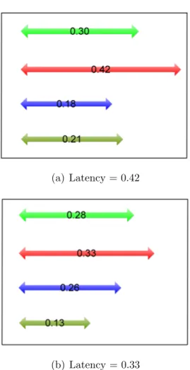
In our case, more durable individuals correspond to heterogeneous NoC ar-chitecture designs are generated with minimum communication latency. For ex-ample, in Figure 3.2, tasks are scheduled to the heterogeneous processors and the second task takes the longest time to finish, which is 0.42 seconds. The arcs indi-cate the execution time of the given task on the mapped processor. This schedule is derived from the individuals shown in Figure 3.1. Then, a new mapping is gen-erated according to the Genetic Algorithm rules. The new communication latency is calculated for the task that requires the longest time to finish. If the commu-nication latency of the newly generated placement is less than the previous one, then we select this placement, which is called the individual. We replace the indi-viduals whose communication latencies are higher in the population with the new individual. It is shown that new communication latency is 0.33 seconds, which is less than the first one; thus, it is selected.
The Genetic Algorithm is composed of 5 important stages: initialization, selection, crossover, mutation, and termination.
3.1.1.1 Initialization
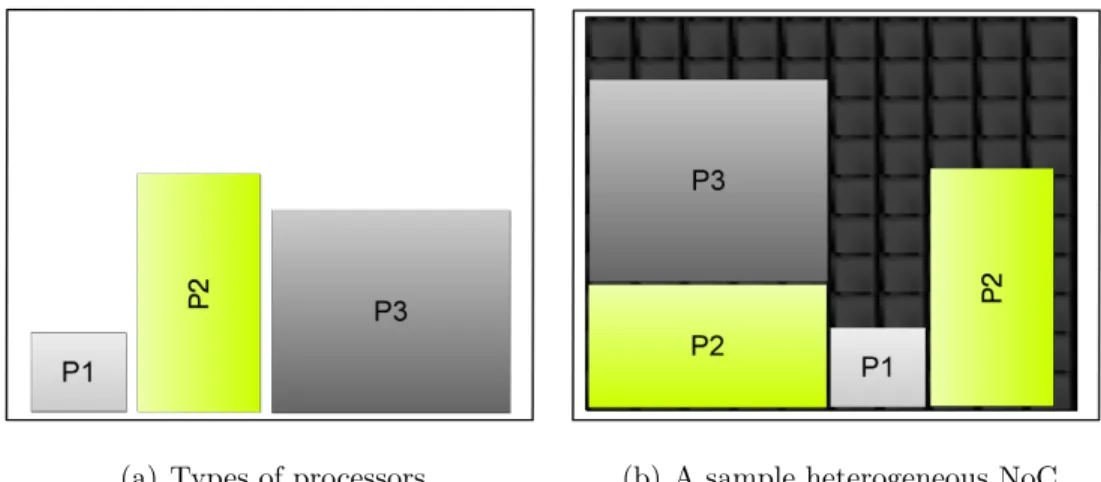
At the beginning of the Genetic Algorithm, a population that consists of ran-domly generated individuals is needed. The number of individuals should be determined intelligently because if it is not selected correctly, the pro-cessing takes longer than the brute force approach. In our experiments, the individuals are represented by the sequence of processors that are as-signed to the nodes. Each appropriate chip design is called an individ-ual. A typical individual has a sequence of processors in the format <Type of processor, height, width, x-coordinate, y-coordinate>. For example, in Figure 3.3 (a), there are three types of processors 1, 2, and 3. In Figure 3.3 (b), four different tasks are assigned to four proces-sors which is called an individual. The representation of an individual is
(a) Latency = 0.42
(b) Latency = 0.33
(a) Types of processors. (b) A sample heterogeneous NoC.
Figure 3.3: Initialization step of the Genetic Algorithm.
(2, 2, 3, 0, 0) ⇒ (1, 1, 1, 3, 0) ⇒ (2, 3, 2, 4, 0) ⇒ (3, 3, 3, 0, 2).
The type of the processor is randomly selected and checked whether it fits into the chip area. Algorithm 1 gives the pseudo-code of the initialization step.
Algorithm 1 Initialization
1: function initialization(Cx, Cy, placedArea, N )
2: CP U ⇒ select randomly
3: if isFit(CP U , placedArea) then
4: placeCPU(CP U , placedArea)
5: initialization(Cx, Cy, placedArea ∪ CP U , N -1)
6: else
7: initialization(Cx, Cy, placedArea, N ) 8: end if
In this stage, isFit() method takes a crucial role because selected processor is sent to isFit() method and it checks point-by-point to determine whether it fits or not. Therefore, to place the next processor into the current heterogeneous NoC layout, we search for an available position starting from the origin all the way to the top right corner of the chip. If we divide the chip area using a regular grid and most of the area is packed, a newly selected processor will check cell-by-cell in the regular grid, where there are even placed rectangles.
3.1.1.2 Selection
After the initialization stage, a set of individuals are selected to generate a new population. The individuals are selected according to their fitness rates, which is a function of f (x). f (x) = max Li/Ck+ T −1 X j=0 Distance(Pk, Pl) × Affin(Ti, Tj) ! (3.1)
In Equation 3.1, k= i mod N, l=j mod N with 0 ≤ i, j < T , 0 ≤ k, l < N , and i 6= j, k 6= l, where T is the number of tasks and N is the number of processors.
Affin(Ti, Tj) is the affinity between the current tasks, which is derived from
TGFF [11] and the distance is calculated using the Manhattan distance function.
Li refers to the load of the ith task and Ck is the capacity of the assigned
processor. Similarly, Pkrefers to the kthprocessor and Ti refers to the ithtask. In
the equation, the distance between a particular processor and the other processors and the affinity of a task on that processor with all other tasks contributes to the communication cost while Li/Ck is the processing cost. Adding communication
cost to the processing cost gives us the overall design cost. Basically, f (x) function gives us the maximum communication latency of a layout for a given set of tasks and processors in the NoC. More specifically, it is the maximum communication latency among individuals in the population. Since, our goal is to minimize the maximum communication latency, we choose individuals that have smaller f (x) values. It is assumed that the fitness values of their children will also be low. In the experiments, we used the roulette wheel technique [14] to select individuals. In the roulette wheel technique, each individual is given a slice of a circular area according to the fitness rate, and then the individuals whose slices are larger are selected. In the experiments, the total cost of each design is calculated and a fitness rate is assigned to each individual according to its communication latency. The individuals that have high latency are selected and the crossover operation is applied to these individuals in order to minimize the maximum latency.
3.1.1.3 Crossover
The next step after individuals are selected is the crossover or reproduction. Be-fore the crossover operation, a crossover point is calculated randomly or reason-ably. Then, the selected individuals are cut according to the crossover point and their parts are used to create a new child. In our implementation, the crossover point is selected as the midpoint and the first half of the first individual is con-catenated with the second half of the second individual to create the first child which is shown in Figure 3.4. In the crossover operation, we check whether the crossover is applicable on that point or not because the processors that come from the other parent may not fit on the chip area because of their dimension. If they do not fit on the chip area, then another point is selected. The new individuals formed as a result of the crossover operation are shown in Figure 3.5.
Figure 3.4: Crossover point selection.
Figure 3.5: The result of the crossover operation.
The details of the crossover operation are given in Algorithm 2. At the be-ginning of the algorithm, crossover is applied to the half of the individuals. If the newly generated individuals are legal, which means they fit properly to the chip area, then these individuals are added to the population and the same number of individuals is excluded from the population whose latency, which we call fitness value, is low.
Algorithm 2 Crossover
1: function crossOver(I1, I2, N, population)
2: for i = 0 upto N/2 do
3: N ew1 = I1[i]
4: N ew2 = I2[i]
5: end for
6: if (N ew1&&N ew2) is legal then
7: population= population+N ew1+N ew2-get2M inimumIndividuals(population)
8: else
9: repeat
10: change crossover point
11: apply crossover
12: until N ew1&&N ew2 is legal
13: end if
3.1.1.4 Mutation
The main idea behind the mutation operation is that a change occurred on an individual without any effect from other individuals may result a stronger in-dividual. Simply, mutation changes some part of the chromosome; in our case, it is the type of the processing core. It is checked whether the new process-ing core fits into the area of an existprocess-ing one. If not, a new type is selected or mutation is just skipped. Consider the first individual given previously; i.e., (2, 2, 3, 0, 0) ⇒ (1, 1, 1, 3, 0) ⇒ (2, 3, 2, 4, 0) ⇒ (3, 3, 3, 0, 2). A mutation for this individual will be applied on a randomly chosen chromosome. Let’s assume the third chromosome, (2, 3, 2, 4, 0), is selected to apply mutation. Then a random processor type is selected; let’s assume it is (1, 1, 1) where its indices correspond to the type, height, and width of the new processing core. Since the dimension of the new processing core is smaller than the old one (i.e., (1, 1) < (2, 3)) the mutation is valid. After the mutation is applied, the new individual becomes (2, 2, 3, 0, 0) ⇒ (1, 1, 1, 3, 0) ⇒ (1, 1, 1, 4, 0) ⇒ (3, 3, 3, 0, 2). We expect these mutation operations generate individuals that minimize communication latency.
3.1.1.5 Termination
These steps are repeated until a termination criterion is reached. The termination criteria are as follows [17]:
• a solution may be generated that satisfies the minimum latency criteria,
• the total number of combinations are applied, or
• the allocated time and cost budget is reached.
Additionally, we also terminate the process if the crossover operation does not generate different children.
3.2
2D Bin Packing
In the initialization step of the Genetic Algorithm given in 3.1.1.1, we assumed the chip is composed of a grid and packing is done grid by grid. To do this, we search for appropriate places for the rectangles on the chip area starting from the origin (0,0). We select the available position starting from the origin to the top right corner of the chip. In our Genetic Algorithm, for each coordinate in the grid, we check whether a processor fits or not. However this exhaustive search becomes impractical with larger dimensions. To overcome the efficiency problems of this approach we implemented a 2D Bin Packing Algorithm.
In the two-dimensional bin packing problem, we are given a rectangular area, having width W and height H, and a set of n rectangular items with width wj ≤ W and height hj ≤ H, for 1 ≤ j≤ n. These rectangles are not identical
they have different properties. The problem is to pack these rectangles into a given area, without overlapping. The items can be rotated or not. According to literature [29], there are four categorization of 2D Packing which are OG, RG, OF, RF.
• OG: the items are oriented (O), i.e., they cannot be rotated, and guillotine cutting (G) is required;
• RG: the items may be rotated by 90◦ (R) and guillotine cutting is required;
• OF: the items are oriented and cutting is free (F);
• RF: the items are oriented and cutting is free (F);
In our approach, we used 2D Bin Packing with RG which allows a 90◦ rotation to achieve a better result compared to Genetic Algorithm.
3.2.1
Problem Formulation and Basic Approach
Here, we formulate the application specific latency-aware layout problem. The notation used is given in Table 3.1.
Table 3.1: The nomenclature for the communication latency calculation.
Notation Definition
ς Task Scheduling Type
τ Set of tasks where τ = t1, t2, t3, ... , tN
πi Set of parent tasks of task i where πi ⊆ τ
LT Communication Latency
Lswitch, Lwire Latency on switch and latency on wire, respectively
θi Finish time of task i
Ti,j Execution time of task i on processing core j
Tnl Total execution time for no-latency consideration
Pi,j Power consumption of task i on processing core j
Pswitch, Pwire Power consumption on switch and power consumption on wire, respectively
PTi,j Power consumption of sending bits from processing
core running task i to processing core running task j pw Wire power per bit for unit length of wire
ps Switching power per bit
dw Wire delay per bit for unit length of wire
ds Switching delay per bit
dss Setup delay for switch
δi,j Distance between processing cores running tasks i and task j
3.2.1.1 Basic Approach
Problem domain is explained in below;
Input
• A chip with dimensions CW and CH.
• A set of processing core types P , including the set of execution times for each tasks, Ti,j for executing Ti on processor Pj and the power consumption
during this execution procedure, Pi,j.
• Maximum number of processing cores that can be used in the placement process.
• A directed acyclic task graph G = (V, E), where V is the set of tasks and E is the set of communication volumes between tasks. An example task graph is shown in Figure 3.6.
Output
• Generate an application specific latency-aware heterogeneous NoC design. This placement ensures that the cores are placed near to their optimal places that minimizes the communication latency for the given tasks graph.
The way of packing processors into the chip area used is presented by Wei et al. [48]. First of all, we are given a set of processor types and their respective features which are shown in Table 3.2.
Table 3.2: Processor types having different dimensions. Type Height Width Capacity Power
P0 5 3 60 20
P1 3 4 80 10
Figure 3.6: Sample task graph representing TGFF task graphs.
First layout is generated indirectly by selecting first set of processors randomly, then these processors are sorted according to their area and used in packing. The number of a specific processor type is determined during the algorithm execution time. After the first placement process, we calculate the communication latency of the current layout according to some criteria which will be examined in more detail in the following sections. For communication latency calculation, we use a task graph which is depicted in Figure 3.6.
General structure of the algorithm is shown in Figure 3.8. In step 1, a set of processor type is determined but how many times a processor will be used is not given and selected randomly. In step 2, selected processors are placed into the chip area according to 2D Bin Packing Algorithm. After the generation of the first layout, task graph is created in step 3 and then mapped into the layout according to task scheduling as shown in step 4. Then the communication latency is calculated for that layout. In each iteration, these steps are repeated without generating a new task graph and the minimum communication latency layout is selected.
Since Wei et al. [48] find local optimal layout, we have improved their al-gorithm for finding global optimal layout by the help of simulated annealing technique. Our base algorithm, which is 2D Bin Packing is called Latency-Aware
Least Wasted First (LA+LWF) and simulated annealing version is called Simu-lated Annealing Least Wasted First (SA+LWF).
3.2.1.2 Problem Formulation
Given set of tasks are represented as a directed acyclic graph. The tasks on the given task graph is represented as τ where τ = t1, t2, t3, . . . , tN, while the
execution time of task i for the specified scheduling scheme ς is represented as Ti,j. For a task that is dependent on some other tasks, the finish time represented
as θi can be calculated as
θi = Ti,j + max ( θk + LTi,k )
where θk is the time to finish of task k that is a parent of task i, i.e., tk ⊆ πi. The
formula tells us that if a task is dependent on some other tasks, it can not start until all the parents finish their execution and send required data to the current task where LTk,i represents the time required to transfer vk,i bits from processing
core that task k is running on the processing core that task i is running on. LTk,i is
referred as communication latency between task k and task i. The contributors to communication latency are time spent on switching element to send vk,i bits and
time spent to sent vk,i bits on wire. This gives us the formula of communication
latency between cores as:
LTk,i = dss + ( ds vk,i ) + ( dw vk,i δk,i)
where δk,i is the distance between the processors that run tasks k and i.
Af-ter finding time to finish all tasks and associated communication latencies, the total execution time of the task graph and total communication latency can be calculated. Total execution time is:
where i = 1, 2, 3, ..., N . On the other hand, total communication latency is:
LT = Ttotal− Tnl,
where
Tnl = max ( Ti,j + max ( θk ) ).
and θk is time to finish task k that is a parent of task i ∈ τ , i.e., tk ⊆ πi. Note
that while evaluating θk for Tnl, we consider all LTi,ks to be zero.
The calculation of the total communication latency is a little tricky if the task graph involves tasks that have more than one parent. When a task has two parents as shown in Figure 3.7, task T 13 has to wait until both tasks T 10 and T 12 finish their execution and pass their data to task T 13. At the time 50 task T 12 finishes its execution and starts sending data to task T 13. It takes 100 time units to send all its data. On the other hand, task T 10 finishes its execution at time 100 and it takes 60 time units to send its data to task T 13. Although the communication latency between T 12 and T 13 is higher than the communication latency between T 10 and T 13, the communication latency between T 10 and T 13 is added to the total communication latency. This is because task T 13 would have to wait task T 10 to finish even it would take no time to receive data from task T 10. While task T 13 is waiting for task T 10 to finish, task T 12 has already sent half of its data to the task T 13. Thus, we have to consider a communication latency after both tasks T 10 and T 12 are finished. At time 100 both tasks T 10 and T 12 are finished and task T 10 starts to send its data to tasks T 13 while task T 12 has already sent half of its data to task T 13. After then, it takes 60 time units for task T 10 to send its data and it takes 50 time units for task T 12 to send its remaining data to task T 13. For this reason the communication latency occurred between task T 10 and T 13 is selected and added to the total communication latency.
When both tasks T 10 and T 12 are finished, it takes LT13,12 - (φ10 - φ12) time
Figure 3.7: A task having two parents.
send its data. Therefore, the parent node that has contribution to the total communication latency can be found as: tk ∈ πi | M AX( θk+ LTi,k ).
Then, total communication latency can be calculated as;
LT = N X i=1 i X k=1 ( Lk,i) !
The power consumption can be calculated in a similar way. The power con-sumed on processing core to run task i is represented as Pi,j. The power
con-sumption of sending vk,i bits from processing core running task k to processing
core running task i can be calculated as:
PTk,i = Pswitch + Pwire,
where
Pswitch = ps vk,i , and Pwire = pw vk,i δk,i.
3.2.1.3 An Example
Here, we demonstrate generation of the heterogeneous NoC topology and place-ment of processing cores based on the given constraints and specifications. Also,
Figure 3.8: The overview of the proposed approach.
we give a numerical example of how the total execution time and total communi-cation latency are calculated based on the formulations given above. The overall process is depicted in Figure 3.8.
At the beginning, the processing cores are selected and placed into the chip area. In this example, the first layout consists of six cores, (P0, 0, 0) → (P1, 0, 3) → (P1, 2, 3) → (P2, 2, 5) → (P2, 3, 5) → (P2, 4, 5) where the parameters represent the processor type, x and y coordinates, respec-tively. After the first layout is generated, the tasks given in the task graph are assigned to the processing cores according to the scheduling scheme specified in Section 3.2.2.4. In this example, the ordered scheduling is applied and we get the layout shown in Figure 3.8. For this layout, we calculate total execution time and communication latency. The total communication latency, LT is Ttotal− Tnl,
and the total execution time is Ttotal= max(θi).
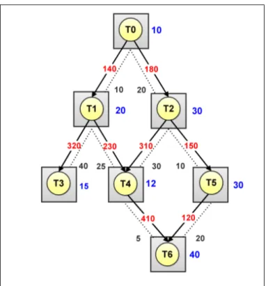
After the scheduling of tasks to the processing cores, we obtain a scheduled task graph as illustrated in Figure 3.9. In this graph, the numbers next to the outer circles represent the execution times for the tasks assigned to the particular processing cores, i.e., Ti,j. The solid directed line represents the communication
volume, i.e., vi,j, and the dashed line represents the distance between processing
cores, i.e., δi,j, that the corresponding tasks are assigned to.
The total execution time is 117.5 that is max(θi), where
θ0 = 10, θ1 = 10 + [20 + (140 × 10−3× 10)] = 31.4, θ2 = 10 + [30 + (180 × 10−3× 20)] = 43.6, θ3 = 31.4 + [15 + (320 × 10−3× 40)] = 59.2, θ4 = 12 + [max(31.4 + 5.75, 43.6 + 9.3)] = 64.9, θ5 = 30 + [43.6 + (150 × 10−3× 10)] = 75.1 and θ6 = 40 + [max(64.9 + 2.05, 75.1 + 2.4)] = 117.5.
Notice that we take dss and ds zero for simplicity and we consider all the wire
links are of the same type and dw as 10−3. After finding the total execution time,
the total communication latency can be calculated as follows:
LT = 117.5 - (10 + 30 + 30 + 40) = 7.5
3.2.2
2D Bin Packing Methodology
The communication latency occurring among communicating processing cores is dominated by wire propagation delays. Intuitively, placing communicating pro-cessing cores as close as possible will reduce this communication latency. Such a placement might seem trivial for a couple of cores and tasks; however, it becomes challenging when the number of processing cores and associated tasks scale up. Finding optimal NoC topology and placement of a given set of processing cores is known as an NP-hard problem [13]. In addition to the complexity of finding proper placement for processing cores, the concerns of task scheduling and other constraints such as power consumption make the problem even more challeng-ing. Thus, we developed heuristics that effectively find near-optimal (i.e., satis-fying the requirements) NoC topology and placement of processing cores within a reasonable amount of time that fulfill the design requirements. Basically, our
Figure 3.9: Scheduled task graph into heterogeneous NoC.
heuristics consist of three main parts:
1. NoC topology generation and placement of processing cores,
2. Scheduling of tasks on processing cores based on the given scheduling scheme,
3. Calculation of the latency and total execution time of the task graph on the proposed layout.
The overall procedure of exploring an application-specific latency-aware het-erogeneous NoC topology and processing core placement is presented in Fig-ure 3.8. The constraints, including the desired chip width, chip height, the max-imum number of processing cores allowed on the given chip area and number of processing core types (i.e., degree of heterogeneity), are given as an input. In addition to these constraints, the task graph associated with the set of applica-tions that is intended to be run on the resulting MPSoC and the specificaapplica-tions
Figure 3.10: The algorithm for exploring an application specific and a latency-aware NoC topology.
of candidate processing cores as well as other subsystem components are also given beforehand. Then, in the first phase, the algorithm evaluates the given constraints and component specifications and generates a NoC topology and pro-poses placement locations of the processing cores. In the second phase, the given task graph is processed based on the specified scheduling scheme, and all tasks are assigned to the processing cores that were determined in the first phase. In the third phase, overall execution time of the task graph and associated commu-nication latency are evaluated. These three phases are repeated until the desired NoC topology and placement of processing cores are found, or the time specified for the algorithm expires. At the end, the algorithm returns the NoC topology and placement of processing cores, which minimizes the communication latency for the given set of processing cores and tasks.
3.2.2.1 NoC Topology Generation
For simplicity, we consider that each processing core is associated with a unique switch that is located at the bottom left corner of the core. Then, we generate candidate topologies for selected processing cores by placing them on a given chip area. Placement of processing cores on a chip area can be treated as a 2D Bin Packing problem, thus, we extended and used the Least-Wasted-First (LWF) 2D Bin Packing Algorithm presented by Wei et al. [48] to generate candidate NoC topologies. In the LWF algorithm, a set of rectangles is selected and stored in an array. The selection of the set of rectangles is repeated a certain number of times. For each set of rectangles different placements are generated. To gener-ate a placement, two rectangles are selected randomly from the array and then swapped. If the new order of rectangles improves the area utilization, the new order is accepted; otherwise, the old order is restored. This process is repeated a certain number of iterations. Since the original LWF algorithm has an objective function of area utilization, it eliminates placements that might minimize the la-tency for the given set of processing cores and tasks. Thus, we modified the LWF algorithm and made it latency-aware. Our modification is twofold:
• improving efficiency of the algorithm by simulated annealing.
To make the placement latency aware, instead of looking at the area utiliza-tion, we look at the latency for the given order. If the new order minimizes the communication latency, then we accept the new order; otherwise we restore the previous order. However, it is possible to be trapped into a local minimum for the current order of processing cores. To overcome this and to improve the efficiency of the algorithm, we further extended LWF and embedded simulated annealing into it. If the new order of the processing cores does not minimize the communication latency, we still accept the new order with some probabil-ity, with the hope of escaping from local minima and reaching global minima. The cooling schedule and acceptance probability function are dependent on the given constraints and some other internal parameters of the algorithm. For the sake of brevity, we do not examine the details of simulated annealing in here but the implementation is given in Appendix C. We evaluate the base algorithm and simulated annealing version in the experimental results section to show its effect. While simulated annealing increases the probability of reaching optimal heterogeneous NoC topology, or at least a better topology than that is gener-ated by the base algorithm, it results with extra computation, which we consider insignificant. Just before generating candidate placements as described above, we must determine which processing cores will be used in the placement. To do that, we pre-process the given constraints and component specifications. First, we eliminate the processing cores that do not fit into the chip area. Then, we select a number of processing cores as specified (i.e., the maximum number of processing cores), ensuring that at least one processing core is selected from each type of processing core. The selected processing cores are used in the algorithm.
Algorithm 3 Heterogeneous NoC topology generation algorithm. for i = 0 to maxSelect do
Fill processor list randomly from processor type list. optimumLayout = Pack processor list into the chip area minimumLatency = Calculate latency for optimumLayout for j to maxSwap do
Select random a, b processors in processor list Swap their position
currentLayout= Pack swapped processor list into the chip area minimumLatency= Calculate latency for currentLayout if currentLatency < minimumLatency then
optimumLayout = currentLayout minimumLatency = currentLatency end if end for end for return optimumLayout
3.2.2.2 Packing Algorithm Details
2D Bin Packing Algorithm details are given in the following subsections.
3.2.2.3 Packing
We have divided packing procedure into 3 phases which is similar to Wei et al. [48]. In their algorithm, initial rectangle set is given and they try to pack all these rectangles at the same time. However, we are given only processor types, so we select processors randomly at the beginning. Selection part is depicted in Algorithm 4.
Algorithm 4 Filling used processor list randomly from processor type list. function selectP E()
while Used Processor List is not full do Select Random PE()
Add Selected PE to Random PE List() end while
After specifying used processor list, packing operation starts. First phase of our algorithm is shown in Algorithm 5.
Algorithm 5 Packing algorithm details - Phase 1.
1: Generate Task List
2: Call Algorithm 4
3: 2D Packing
1: bestLayout = Algorithm 6(P rocessorList)
2: minimumLatency = CalculateLatency(bestLayout)
3: for i = 0 upto maxSelect do
4: newLayout = Algorithm 6(P rocessorList)
5: newLatency = CalculateLatency(newLayout)
6: if newLatency < minimumLatency then
7: select newly generated Layout
8: end if
9: Call Algorithm 4
10: end for
As it is explained in Algorithm 5, our algorithm starts by generating a task graph. This task graph is generated only once and same task graph is used during the execution time of the algorithm to obtain comparable results. After task graph generation, processors are selected according to Algorithm 4. After the initial settings, algorithm tries to find optimal layout which generates minimum latency by the help of Phase 2 which is shown in Algorithm 6. In these algorithms, maxSelect and maxSwap are the number of iterations which depend on the processors that will be used in the packing.
Algorithm 6 Packing algorithm details - Phase 2.
1: Sort the randomly generated processor list w.r.t their area
2: Swap wi and hi if wi is smaller than hi
3: for i = 0 upto P rocessorList do
4: Call Algorithm 7(P rocessor[i], bestLayout)
5: end for
6: minimumLatency=CalculateLatency(bestLayout)
7: for i = 0 upto maxSwap do
8: Select random a and b
9: Swap(SortedP rocessorList, a, b)
10: newLayout = Algorithm 7(P rocessorList)
11: newLatency = CalculateLatency(newLayout)
12: if newLatency < minimumLatency then
13: select newly generated Layout
14: else
15: Swap(SortedP rocessorList, a, b)
16: end if
17: end for
Phase 2 is similar to Phase 1, the only difference is the swap operation and generating new random processor list. In phase 2, we sort processor list and swap width and height when width is greater than height. We do not generate a new processor list in each iteration which is done in Phase 1. It is generated only once and used during Phase 2. On the other hand, the packing process is done at Phase 3.
Figure 3.11: Feasible points for the current heterogeneous NoC layout.
Algorithm 7 Packing algorithm details - Phase 3.
1: Sort packed processors w.r.t getX() plus getW (). If it ties sort w.r.t getY () plus getH()
2: Find feasible points similar to Martello et al. [29]
3: Calculate wasted area for the processor for each feasible point
4: If wasted areas tie then assign Goodness Number shown in Table 3.3 for those points
5: Then select the smallest Goodness Number and pack that processor into that feasible point
Packing procedure details are given in Algorithm 7. The way of finding feasible points is taken from Martello et al. [29] and shown in Figure 3.11. For each feasible point, we calculate the wasted area and if the wasted area is the same, then we assign a Goodness Number shown in Table 3.3.
In Table 3.3, PH is the height of the current processor that we try to pack
and FH is the height of the current feasible point. For communication latency
calculation, we use task scheduling algorithms which is explained in the section 3.2.2.4.
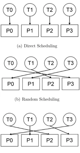
3.2.2.4 Task Scheduling
Scheduling tasks to the processing cores is performed based on the specified scheduling scheme. Our algorithm is highly flexible in this regard. It is pos-sible to integrate any scheduling scheme/algorithm with no complications. We use three scheduling algorithms:
• Ordered scheduling,
• Random scheduling,
• Minimum execution time scheduling.
In ordered scheduling, the given tasks are scheduled to processing cores in order. The first task is assigned to the first processing core, the second task is assigned to the second processing core, and so on. In the event that there are more tasks than the number of processing cores, scheduling returns to the first processing core and continues until all tasks have been assigned to a processing core.
In random scheduling, the given tasks are randomly scheduled to processing cores. To prevent under-utilized processing cores (i.e., cores that has no task assigned) we use a dynamic list. After filling the list with processing cores we assign next task to a processing core randomly. Then, we remove that processing
Table 3.3: Goodness numbers used to decide the placement of the current pro-cessor. GN PH vs FH PW vs FW 1 == == 2 == < 3 < == 4 < < 5 == > 6 > == 7 > < 8 < > 9 > >
(a) Direct Scheduling
(b) Random Scheduling
(c) Minimum Execution Time Scheduling
core from the list. If there are still unassigned tasks when the list is empty, we fill the list again and proceed as described.
In minimum execution time scheduling, the given tasks are scheduled to cessing cores according to the execution times. Each task is assigned to a pro-cessing core that will run the task faster than the others. Similar to random scheduling, we use a dynamic list to prevent under-utilized and/or over-utilized processing cores.
3.2.2.5 Latency Calculation
After all tasks are scheduled, we calculate the total communication latency and execution time of the given task graph as described in section 3.2.1.
Experimental Results
We implemented our application specific latency-aware heterogeneous NoC design algorithm in Java, and performed the experiments in two different machines. The first machine was an AMD PhenomII X6 1055T with 4GB of main memory on a Linux kernel 2.6.35-24. The second machine was an Intel Pentium Dual-Core E6500 with 2GB of main memory on a Linux kernel 2.6.35-28.
Experimental results consist of Genetic Algorithm and 2D Bin Packing Al-gorithm results. Genetic AlAl-gorithm results are given first, followed by 2D Bin Packing experimental results with two different categories. In the first category, we aimed to show that the 2D Bin Packing Algorithm that we extended is compet-itive with well-known packing algorithms. During these experiments we did not consider the total execution time of the task graph and communication latency of the generated NoC, but considered the packing efficiency in terms of dead areas that could not be utilized for packing. For this category, we performed each set of experiments 10 times and took the average. The Intel machine was used for this category of experiments.
In the second category, we aimed to show that the application specific latency-aware heterogeneous NoC design algorithm that is based on the extended LWF bin packing algorithm generates heterogeneous NoC topology and places processing cores on a given chip area such that the total execution time and communication
latency of the given task graph are minimized considering the given constraints and fulfill the requirements of the desired MPSoC. In this category, we performed four sets of experiments for different benchmarks and settings. Again, we per-formed each set of experiments 10 times and took the average. The AMD machine was used for this category of experiments.
4.1
Experimental Results of Genetic Algorithm
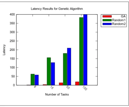
We evaluated the given algorithm for the tasks that are generated by TGFF software. We evaluated two random layouts in which tasks and processor types are fixed (i.e., Random1, and Random2). We have four sets of tasks with different number of tasks in each set. We compared Genetic Algorithm with two different Random Algorithms. In Random 1, processing elements are fixed and same processors are used. Whereas in Random 2, tasks are fixed. We have fixed these two parameters in order to make controlled experiment. Each set was tested 1000 times to get admissible results. We have used 4 different task graphs containing 8, 16, 50, and 100 tasks, respectively.
Figure 4.1 gives the execution latency results for Random1, Random2, and Genetic Algorithm with various number of tasks ranging from 8 to 100. Genetic Algorithm outperforms both Random1 and Random2 implementations. As can be seen from this graph, our approach performs much better as the number of tasks increase. One can observe that it is critical to have an effective heterogeneous NoC design with higher number of tasks.
Figure 4.1: Latency comparison of Genetic Algorithm with random algorithms.
4.2
Experimental Results of 2D Bin Packing
Al-gorithm
4.2.1
Packing Efficiency
In this category of experiments, we showed that LWF bin packing algorithm that we used is competitive with well known bin packing algorithms in terms of both area utilization and execution time. We compared LWF with Parquet [1], B∗− tree [6], TCG-S [28] and BloBB [5] algorithms. We used a benchmark called Floor-planning Examples with Known Optimal Area (FEKO-A) [40] that is an extended version of MNCN benchmarks [49]. The FEKOA consists of the circuits that are shown in Table 4.1.
The performance of the LWF bin packing algorithm is very competitive, as seen in Table 4.2.11. For the first three circuits LWF finds the optimal layout (i.e., zero dead area), as BloBB does. For FEKOA4 and FEKOA5 it performs
1The experiments with LWF were run on a 2800 MHz 6-Core AMD Phenom II X6 processor,
Name Circuit Number of blocks FEKOA1 apte 9 FEKOA2 hp 11 FEKOA3 xerox 10 FEKOA4 ami33 33 FEKOA5 ami49 49 FEKOA6 n300 300 FEKOA7 ami49 x10 490 FEKOA8 n300 x10 3000
Table 4.1: FEKOA benchmark content.
Circuit Parquet B*-tree TCG-S BloBB LWF
Dead space (%) Run-time (sec) Dead space (%) Run-time (sec) Dead space (%) Run time (sec) Dead space (%) Run-time (sec) Dead space (%) Run-time (sec) FEKOA1 14.36 0.03 4.76 0.65 5.40 0.4 0.00 0.01 0.00 0.50 FEKOA2 9.69 0.04 6.74 0.10 8.66 0.5 0.00 52.48 0.00 0.55 FEKOA3 11.31 0.03 3.95 0.44 3.61 0.4 0.00 4.91 0.00 0.48 FEKOA4 6.26 0.25 2.32 24.16 4.62 8.7 4.58 1.12 3.88 3.04 FEKOA5 5.55 0.54 2.05 46.29 4.80 24.0 6.56 23.34 3.62 6.48 FEKOA6 9.11 28.04 8.99 47.85 10.98 392.3 8.56 7.51 3.99 799
Table 4.2: The performance comparison of LWF with well-known packing algo-rithms.
much better than Parquet and BloBB; however slightly worse than B∗ − tree. We experienced that this is due to the lower number of iterations on LWF to keep execution time as close to the other algorithms as possible. If we run LWF with a higher number of iterations, it is also superior to the B∗− tree algorithm for FEKOA4 and FEKOA5, but at the expense of increased algorithm execution time. This is the case in FEKOA6 where LWF outperforms in terms of dead area, but it takes longer compared to other algorithms.
Overall, we can infer that the LWF bin packing algorithm is competitive and suitable for use in floor-planing applications. As mentioned in previous sections, the iterative nature of LWF enabled us to leverage it. We extended LWF such that it takes into account communication latency on the resulting layouts and
proceeds accordingly in each iteration, leading to a heterogeneous NoC design that minimizes total execution time and communication latency of the given task graph.
4.2.2
Application-specific Latency-aware Heterogeneous
NoC Design
In this category of experiments, we show that the presented application-specific latency-aware heterogeneous NoC design algorithm generates an NoC topology and places the processing core on a given chip area such that total execution time and communication latency are minimized for the given task graph. The algorithm also considers the given constraints and fulfills the desired MPSoC requirements. Considerations include keeping power consumption at acceptable levels and increasing chip area utilization as much as possible.
We perform four sets of experiments in this category. In the first set, we show that NoC designs that try to maximize chip area utilization without considering latency as a first-class concern result in higher total execution time and commu-nication latency. We compare our application-specific latency-aware NoC design algorithm with CompaSS [4], which is known as a powerful packing algorithm for NoC design. In this set of experiments, we use MCNC benchmarks with different settings.
In the second set, we compare our application-specific latency-aware NoC design algorithm with task scheduling and core-mapping algorithms. Such algo-rithms consider that NoC is fixed and given beforehand. As we claim earlier, to achieve the desired MPSoC, one must consider task scheduling, core map-ping and NoC topology generation as a whole. We present a set of results here to show that task-scheduling and core-mapping algorithms such as NMAP and A3MAP do not minimize total execution time and communication latency since they are oblivious to the NoC requirements of desired MPSoCs. We conceive that our work is complementary to task-scheduling and core-mapping efforts such as NMAP and A3MAP and will result in MPSoCs that minimize total execution
time and communication latency. In this set of experiments, we use Embedded System Synthesis Benchmarks Suite (E3S) [12] with different settings.
In E3S benchmarks, there are 45 different tasks and 17 different processors. This benchmark suite contains task graphs for five embedded application types: automotive/industrial, consumer, networking, office automation and telecommu-nications. There is a version of each task graph for three kinds of systems: distributed (cords), wireless client-server (cowls) and system-on-chip (mocsyn). An application is described by a set of task graphs. The task types are shown in Appendix B.1 and processor types are given in Appendix B.2. The task graphs from E3S are directed acyclic graphs; they have a period and deadlines may be set on tasks. The period of a task graph is defined as the amount of time between the earliest start times of its consecutive executions. A deadline is defined as the time by which the task associated with the node must complete its execution. Each task graph is described using an ASCII file in the TGFF format.
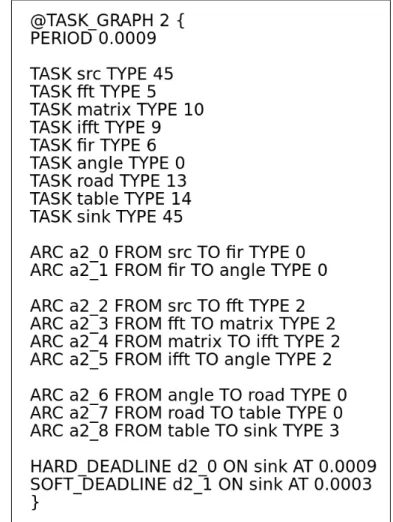
Figure 4.2: The task graphs from the auto-indust-mocsyn benchmark.
For example, Figure 4.2 shows 3 different task graphs from the auto-indust-mosyn benchmark. The task graph shown in Figure 4.3 is described in the fol-lowing way:
Figure 4.3: Textual representation of the task graph 2 from the benchmark auto-indust-mocsyn.
It can be observed that there are two main elements in the task graph descrip-tion file shown in Figure 4.3: TASK and ARC. Both of them are characterized by the TYPE attribute (which is a number). For the ARC element, the TASK attribute specifies the amount of communication required by the data exchange between the interconnected tasks. The values which correspond to each TYPE of ARC are specified in the same TGFF file: