Arrays of Suspended Plasmonic Nanodiscs
Can Uran1 and Hilmi Volkan Demir1,21Department of Electrical and Electronics Engineering, Department of Physics, and UNAM - Institute of Materials Science and Nanotechnology
Bilkent University, Ankara, Turkey TR-06800
2LUMINOUS! Center of Excellence for Semiconductor Lighting and Displays, Microelectronics Division, School of Electrical and Electronics
Engineering and Physics and Applied Physics Division, School of Physical and Mathematical Sciences, Nanyang Technological University, Nanyang Avenue, Singapore 639798, Singapore
Email: [email protected] and [email protected]
Abstract: We demonstrate lateral arrays of suspended metal nanodiscs, erected in parallel,
partially encased in a dielectric-wrap using in-template synthesis with their polarization-dependent properties controlled as a function of disc-gap/-width tailoring their scattering/absorption spectra.
Plasmonic structures enable enhanced light utilization for optoelectronic devices owing to their unique, strong and tunable electric field localization leading to increased scattering and absorption properties. Various nanopatterned plasmonic structures have been proposed to date, which typically use the nanofabrication method of electron beam lithography (EBL). Although these techniques offer high resolution and allow for a more deterministic nanostructure layout for plasmonics, these technologies are quite costly and limited in high throughput. Alternatively, solution processed nanostructures have emerged, for example, including nanodiscs [1], which are synthesized using in-template electro-deposition [2], followed by simple selective etching of sacrificial metal layers. These nanodiscs are promising for nanoplasmonics because their optical properties may be fine-tuned either via the gap or the disc-width, which can range from 20 nm to several hundred nanometers. In this work, we demonstrate lateral arrays of Au nanodiscs with controlled gaps and widths using the in-template synthesis to allow for the tailoring of the scattering and absorption properties. This has resulted in massive numbers of easily and inexpensively fabricated arrays of nanodisc structures. The achievable resolution of our fabrication approach reaches down to approximately 20 nm. Fabricating such three-dimensional suspended and liquid dispersible architectures is not easily possible by other techniques such as EBL. Here, we report the plasmonic properties of these suspended nanodisc structures including the polarization-dependent scattering spectra computed numerically and measured experimentally.
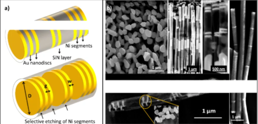
Fig. 1. (a) Illustration of the suspended plasmonic nanodisc array fabrication using in-template synthesis. (b) SEM images of the suspended gold nanodisc array fabrication steps from in-template synthesis of segmented nanowires to selective etching of Ni segments leaving
behind arrays of suspended gold nanodiscs inside SiN dielectric-wrap.
We study the polarization dependent absorption and scattering properties of the nanodisc arrays presented in Fig. 1(a) and 1(b). We model our discs to tailor the light spectra scattered from and absorbed in these Au discs with varying disc-widths (w) for different disc gaps (g). Under unpolarized illumination incident on discs, we observe different spectral contributions from the field polarized in vertical and horizontal directions. Figs. 2(b) and 2(c) present the computed quality scattering factors of the nanodisc array via power fraction analysis of vertically and horizontally polarized fields. Here the disc diameter (D) is 250 nm, which is set by our template membrane used during electro-deposition. When we compute the power component normal to the discs (vertical), we observe strong plasmonic coupling depending on the gap size (g) between the discs. The electric field localized between the discs is found to increase with this coupling. We observe a scattering peak at shorter wavelengths in Fig. 2(b) with a disc width (w) of approximately 50 nm and above. When we compute the power component along the plane of the disc (horizontal), we do not observe strong coupling between the discs in this direction. With 250 nm disc diameter (D), we observe scattering at longer wavelengths in Fig. 2(c).
558 WH2.4 (Contributed)
11:15 AM – 11:15 AM
For the in-template synthesis of the gold nanodisc array, we used a porous alumina membrane as the template, with a pore size of approximately 250 nm, and electro-deposited Au and Ni segments into the pores of the membrane at a driving current level of -1.6 mA, alternating Ni and Au baths (Orotemp Italgalvano), using a Versastat3 potentiostat. Ni segments served as the sacrificial layers, which determine the gap size between the Au nanodiscs after selective etching. Controlling the amount of charge passing through the pores of the membrane, we fabricated discs with size controllable widths. After the deposition of each disc, the structure was annealed at 250 °C to form more uniform discs and gaps. Completing the deposition steps, the alumina membrane was dissolved in sodium hydroxide solution (3 M), while the deposited segments remained together in the base solution during dissolution. Subsequently, they were centrifuged in water. Au and Ni segments were further immobilized on a glass slide by drop casting and a 50 nm thick SiN dielectric film was deposited on them by plasma enhanced chemical vapour deposition (PECVD), partially wrapping them as a blanket-layer. After the sonication of these glass slides, one side coated segments were detached from the glass surface and dropped into solution [3]. Sonication time was found very critical not to damage structure with Au discs kept firmly inside the SiN support. The sacrificial Ni segments were finally selectively etched in 30% nitric acid solution, leaving behind arrays of suspended Au nanodiscs kept together in a partial SiN dielectric-wrap (Fig. 1(b)).
Fig. 2. (a) Lumerical simulation setup. Scattering quality factor under unpolarized illumination: spectral contribution of (b) vertically and (c) horizontally polarized fields for varying disc-width (w) at different disc gaps (g).
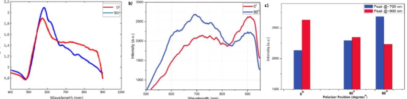
We present the vertical and horizontal modes scattered from the nanodiscs on quartz in Fig 3(a) as numerically computed, and in Fig 3 (b) as experimentally measured. For the vertical component (for which the polarizer was positioned normal to the nanodiscs), we observed scattering stronger in the short wavelength range and weaker in the long wavelength range (blue line). On the other hand, for the horizontal component (for which the polarizer was positioned in the plane of the nanodiscs), we observed scattering stronger in the long wavelength range and weaker in the short wavelength range (red line). Compared to the computed scattering spectra, the red-shift in the experimental data stems from the nanodiscs being placed on quartz substrate in the experimental measurements. Intensity of these peaks changes with respect to the position of the polarizer located at the light collection (Fig 3(c)).
Fig. 3. Scattering spectra of a single suspended Au nanodisc array on quartz parameterized (a) numerically computed and (b) experimentally measured with the position of the polarizer varied from 0° (vertical orientation) to 90° (horizontal orientation) with respect to the normal of the
nanodiscs. (c) Changes in intensity peaks with the position of the polarizer varied from 0° to 90°.
In conclusion, using plasmonic nanodisc arrays, we observed the vertical and horizontal components of the scattered light sensitive to the disc size parameters such as width, diameter and gap. These developed plasmonically tunable nanostructures offer applications in photodetection with polarization sensitivity.
References
[1] S. Lui et al., Nano Lett. 5, 1071-1076 (2005). [2] C. Uran et al., IEEE JSTQE, 15, 1413-1419 (2009). [3] L. Qin et al., Science, 309, 113 (2005).
559