ENHANCING LIGHT EXTRACTION EFFICIENCY OF
InGaN/GaN MULTI QUANTUM WELL LIGHT
EMITTING DIODES WITH EMBEDDED TWO
DIMENSIONAL PHOTONIC CRYSTAL
STRUCTURES
A THESIS
SUBMITTED TO THE GRADUATE PROGRAM OF MATERIALS SCIENCE AND NANOTECHNOLOGY
AND THE INSTITUTE OF ENGINEERING AND SCIENCES OF BILKENT UNIVERSITY
IN PARTIAL FULLFILMENT OF THE REQUIREMENTS FOR THE DEGREE OF
MASTER OF SCIENCE
By
Ali Güneş KAYA August 2010
I certify that I have read this thesis and that in my opinion it is fully adequate, in scope and in quality, as a thesis for the degree of Master of Science.
Prof. Dr. Salim Çıracı (Supervisor)
I certify that I have read this thesis and that in my opinion it is fully adequate, in scope and in quality, as a thesis for the degree of Master of Science.
Res. Asst. Prof. Dr. Aykutlu Dâna (Co-supervisor)
I certify that I have read this thesis and that in my opinion it is fully adequate, in scope and in quality, as a thesis for the degree of Master of Science.
I certify that I have read this thesis and that in my opinion it is fully adequate, in scope and in quality, as a thesis for the degree of Master of Science.
Asst. Prof. Dr. Ali Kemal Okyay
Approved for the Institute of Engineering and Sciences:
Prof. Dr. Levent Onural
ii However, potential performance of III-Nitride based devices is hindered mainly because of an optical phenomenon called total internal reflection (TIR). High dielectric constant of these materials prevents light to escape from the structure. Light is totally reflected back from the air-nitride interface for incident angles larger than critical angle. With a refractive index of 2.7, GaN material has 22°-24° critical angle which means less than 12% of light can just
ABSTRACT
ENHANCING LIGHT EXTRACTION EFFICIENCY OF InGaN/GaN MULTI
QUANTUM WELL LIGHT EMITTING DIODES WITH EMBEDDED TWO
DIMENSIONAL PHOTONIC CRYSTAL STRUCTURES
Ali Güneş KAYA
M.S. in Graduate Program of Materials Science and Nanotechnology Supervisor: Prof. Dr. Salim Çıracı
August 2010
Advance in the growth methods of III-Nitrides and researches in order to eliminate doping problems of gallium nitride (GaN) resulted in high band gap materials with increased crystal quality which have led to tremendous improvement in opto-electronic devices. Their durability under harsh environmental and operational conditions such as high pressure and high temperature, and large spectral coverage range including 200 nm deep ultra-violet (deep-UV) through 1500 nm infra-red (IR) make them excellent candidates for opto-electronic applications such as full color LCD panels, biomedical sensor devices, high resolution printers, high density storage devices, defense systems. Among III-Nitrides, GaN has attracted the most interest with its high electronic band gap of 3.4 eV at room temperature and ability to form compounds with other group III elements aluminum and indium which have band gaps of 6.2 eV and 0.7 eV respectively which results in a large optical spectrum.
iii escape the structure. While 66% of the light generated in quantum well region of a GaN based light emitting diode (LED) is trapped in the GaN layer, 22% of the light is guided in the sapphire substrate. Because of TIR, although internal quantum efficiency of GaN based LED with emission wavelength of around 400 nm is almost unity (higher than 90%), external quantum efficiency is very low. To enhance extraction, a lot of geometrical methods including surface roughening and facet shaping have been tried to reduce the effects of dielectric contrast between the device and medium.
In order to increase the extraction efficiency of GaN based LEDs, two dimensional photonic crystals were used in this thesis. LED wafers used were fabricated in collaboration with University of Santa Barbara, California (UCSB) which are InGaN/GaN multi quantum well (MQW) structures that emit light at 390 nm and 410 nm respectively. These LED wafers were processed in the scope of the thesis and photonic crystal (PC) structures were patterned on the p layer of the device.
This thesis work is concentrated on two parts; first part is characterization and fabrication, and second part is simulation. In characterization and fabrication part, firstly GaN material etching characterizations were completed using dry etching method by reactive ion etcher (RIE) since there had been no optimized recipe for GaN processing in the clean room know-how. In this characterization, main parameter was the etching anisotropy since vertical side-wall is crucial for LED processing and PC formation. After characterization step was completed, p doping activation was done in Middle East Technical University, Ankara (METU) and then LED wafers were processed in clean room class-100 environment at Bilkent University, Ankara by using the know-how and recipe obtained from characterization stage. As a final step, two dimensional square and triangular photonic crystal lattice structures were patterned by using electron beam writer and these structures were transferred on to p layer of GaN LED by using RIE. Measurements and imaging regarding material and optical properties, fabrication quality and extraction enhancement were done by using scanning electron microscope (SEM), atomic force microscopy (AFM), spectrophotometer (UV-Vis), ellipsometer and probe station. I-V characteristics, optical power measurements and intensity plots on black&white CCD camera images were taken. In simulations part, two and three dimensional simulations using plane wave expansion method, integral method and finite difference time domain method were completed. More than 40000 simulations were run in total during this thesis work.
As a result, PCs with 520 nm lattice period and 260 nm hole diameters in square and triangular geometries were modeled and fabricated. Final depth of lattices was around
100-iv 120 nm. Results of 2D integral simulations suggested around 15-20% of error between modeling and experiments because of imperfectness regarding fabrication of PC structures. Furthermore, damaging effects of RIE and focused electron beams were not considered. In measurements, extraction efficiency enhancement factors of about 2.2 and about 2.6 were found using square and triangular PC lattices with respect to LED devices without PC structure patterning. In simulations, while square PC lattice models showed 2.8 times enhancement in extraction efficiency, triangular lattice resulted in 3.1 times with respect to no PC models. In comparison of measurements and simulations, difference in the range of 15-25% was found which were expected as stated above with also considering the effect of processing damages on top p and p++ layer and quantum well region.
Keywords: Gallium nitride (GaN), Light emitting diode (LED), Photonic crystal, Finite difference time domain (FDTD) simulation
v Ancak, III-nitrürlerin potansiyel olarak sahip oldukları performans, yüksek kırılma indisleri nedeniyle oluşan tam yansımadan dolayı ketlenmektedir. Kırılma indisi 2.7 olan galyum nitrür içinde yol alan ışık, gelme açısı 22° ila 24° arasında olan kritik eşikten fazla olması durumunda hava-galyum nitrür sınırından geçememekte ve gerisingeriye malzeme içine yansımaktadır. Bu durumda, galyum nitrür tabanlı ışık saçan diyotların kuvantum kuyularında üretilen ışığın yalnızca %12’den daha az bir kısmı cihaz dışına çıkabilmektedir. Bu ışığın %66’lık büyük bir kısmı galyum nitrür içinde hapsolmakta, %22’lik bir kesimi ise taban
ÖZET
İKİ BOYUTLU FOTONİK KRİSTAL YAPILARI GÖMÜLÜ InGaN/GaN
ÇOKLU KUANTUM KUYULU IŞIK SAÇAN DİYOTLARIN IŞIK
ÇIKARIM VERİMLERİNİ ARTIRMA
Ali Güneş KAYAMalzeme Bilimi ve Nanoteknoloji Lisansüstü Programı Yüksek Lisans Tez Yöneticisi: Prof. Dr. Salim Çıracı
Ağustos 2010
Büyütme tekniklerindeki gelişmeler ve katkılama problemlerinin çözümü sonrasında büyütülen yüksek kristal kaliteli galyum nitrür başta olmak üzere III-Nitrürler, optronik teknolojisinin gelişmesinde önemli rol oynamışlardır. Uçdeğerlerdeki çevresel şartlar ve çalışma şartları altında dahi yüksek verimle çalışmaları ve 200 nm ila 1500 nm arasını kapsayan optik spektrumları sayesinde optronik uygulamalar konusunda vazgeçilmez hale gelmiş olup şu anda LCD panellerin arka aydınlatmaları, biyomedikal sensor uygulamaları, yüksek çözünürlükteki lazer yazıcılar, yüksek depolama alanlı optik diskler ve savunma sistemleri başta olmak üzere birçok alanda kullanılmaktadırlar. III-Nitrürler arasında en fazla ilgiyi 3.4 eV’luk yüksek elektronik bant genişliğiyle galyum nitrür çekmektedir. Bu bileşiğin diğer Nitrür elementleri olan alüminyum ve indiyum ile bağ yapabilme potansiyeli, III-Nitrür bazlı optronik cihazların kapsadığı optik spektrumu oldukça geniş bir hale getirmiştir.
vi malzeme olan safir içinde yönlenmektedir. Her ne kadar 400 nm civarında ışık saçan galyum nitrür tabanlı diyotların öz kuvantum verimleri %90’dan fazla ise de, tam yansıma nedeniyle dışsal kuvantum verimleri oldukça düşmektedir. Bu durumu bertaraf edebilmek adına geometrik tabanlı birçok yaklaşım denenegelmiştir.
Bu tez çalışmasında, galyum nitrür tabanli ışık saçan diyotların ışık çıkarım verimlerini artırmak için iki boyutlu fotonik kristal yapıları kullanılmıştır. Bu bağlamda, Kaliforniya Santa Barbara Üniversitesi işbiliğiyle Amerika’da büyütülen ve 390 ve 410 nm’de ışıyan galyum nitrür tabanli malzemeler, Orta Doğu Teknik Üniversitesi ve Bilkent Üniversitesi’nde işlenmiş olup ardından fotonik kristal yapıları p katkı malzemeli katman üzerine basılmıştır. Bu tez iki ana çalışmadan oluşmuştur. Bu çalışmalardan bir tanesi karakterizasyon ve üretim çalışmalarıyken diğer çalışma simülasyon ve modellemeleri kapsamaktadır. Karakterizasyon ve üretim aşamasında öncelikle galyum nitrür malzemesinin reaktif iyon delme (RIE) sistemiyle işlenmesi karakterize edilmiştir. Temel karakterizasyon parametresi olarak delinme işleminin eşyönsüzlüğü dikkate alınmıştır. Bu sayede, mümkün olan en dik duvar oluşturacak şekilde işlem karakterize edilmiştir. Karakterizasyon bölümünün tamamlanmasının ardında p tipi katkılama aktivasyonu Orta Doğu Teknik Üniversitesi’nde yapılmıştır. Ardından Amerika’da üretilmiş olan bu malzemelerin ışık saçan diyot üretimi sürecindeki işlemler Bilkent Üniversitesi bünyesindeki sınıf-100 mertebesinde bulunan temiz odada yürütülmüş ve karakterizasyon sırasında edinilen bilgiler ışığında diyot üretimi başarıyla tamamlanmıştır. Son bir basamak olarak fotonik kristal yapıları karesel ve üçgensel geometrilerde olmak üzere elektron ışını yazıcısında diyotlar üzerine basılmış ve reaktif iyon sisteminde son halini almıştır. Son ürünler üzerinde ölçümler prob istasyonu vasıtasıyla yapılmıştır. Bu ölçümler I-V karakteristiği, optik güç ölçümü, siyah beyaz CCD kamerada çekilen fotoğraflardan elde edilen ışık yoğunluğu olarak sıralanmıştır. Simülasyonlar ise iki boyutta ve üç boyutta yapılmış olup düzlem dalga açılımı metodu, integral metod ve sonlu zaman aralıklı etki alanı (FDTD) metodu kullanılarak tamamlanmıştır. Bu tez çalışması süresince, 40000’den fazla simülasyon sonucu değerlendirilmiştir.
Sonuç olarak 520 nm periyotlu, 260 nm çaplı fotonik kristal yapıları üçgensel ve karesel geometrilerde ışık saçan diyot üzerine basılmış ve aynı geometriler bilgisayar ortamında modellenerek simüle edilmiştir. Ortalama fotonik kristal derinligi 100 ila 120 nm’dir. İki boyutlu integral metodu kullanılan simülasyonların sonuç değerlendirmesinde, deneysel ölçümlerle üç boyuttaki simülasyon sonuçları arasında %15 ila %20’lik bir fark olacağı ögörülmüştür. Bu farkın temel kaynağının ise üretilen fotonik kristal şekillerinin dizayn
vii edilenden belirli tolerans dahilinde farklı olmasıdır . Bu toleransa RIE ve elektron ışın demetiyle yazım işlemi dahil edlmemiştir. Ölçümler sonucunda fotonik kristal yapılı diyotların ışık artırım miktarı kare ve üçgen geometriler için sırasıyla 2.2 ve 2.6 kat olarak bulunmuştur. Simülasyon sonuçlarında ise ışık miktarı kare ve üçgen geometrili kristal yapıları icin 2.8 ve 3.1 kat artış görülmüştür. Ölçümler ve deneyler karşılaştırıldığında ortaya çıkan %15 ila %25 arasındaki fark iki boyutlu integral metoduyla yapılan simülasyonda öngörülen farkla örtüşmekte, fazladan %5’lik kesim ise RIE ve electron ışın demetiyle yapılan işlemler sırasında kuvantum kuyularına ve p ve p++ katmanlarına verilen zararın sonucu olarak yorumlanmıştır.
Anahtar kelimeler: Galyum nitrür (GaN), Işık saçan diyot (LED), fotonik kristal, sonlu zaman aralıklı etki alanı (FDTD) simülasyonu
viii
ACKNOWLEDGEMENTS
I would like to thank to my supervisor Prof. Dr. Salim Çıracı, co-advisors Asst. Prof. Dr. Aykutlu Dâna and Asst. Prof. Dr. Bilge İmer for their interest in this thesis.
I also thank to Mustafa Ürel for his help and contribution.
I thank to my group members Hasan Güner, Burak Türker, and Okan Ekiz.
Special appreciation goes to my dear, Ebru. Without her support and encourage, this thesis process would be much harder to complete, especially for the last 1.5 years. Thanks for staying with me in my hardest times, thanks for being in my life.
And finally, I appreciate all the efforts my family has done for me so far, from the very beginning since 1983. They have always been there, by my-side. They have always believed in me, even more than I do. It would not be possible to realize this thesis without their existence. Thanks for bearing me in my most stressful moments. Thanks for being much more than a family to me.
ix Aileme…
sevgili annem Süveyda’ya, değerli babam Osman’a,
güzeller güzeli kız kardeşim Sıla’ya,
x Ebru,
Eb,
Ebbie, Beb,
1
Table of Contents
1. Introduction ... 11
2. Gallium Nitride & Material Properties ... 15
2.1 Introduction ... 15
2.2 Direct & Indirect Band Gap Structures ... 15
2.3 III Nitrides Background ... 16
2.4 Growth of GaN ... 18
2.5 Structure of InGaN/GaN QW LED wafer grown by collaboration with UCSB ... 21
2.6 Chemical and Physical Properties of GaN ... 21
2.6.1 Band Gap of GaN and InN ... 23
2.6.2 Bonding Structure ... 23
2.6.3 Crystal Structure ... 24
2.7 Impurities in GaN ... 25
2.7.1 Doping ... 28
2.7.2 Defects in GaN ... 29
2.7.3 Defect related Illumination Peaks seen on GaN ... 31
2.8 Polarization Issues and Quantum Confined Stark Effect (QCSE) ... 31
3. Light Emitting Diodes and InGaN/GaN Multi Quantum Wells ... 33
3.1 Introduction ... 33
3.2 Background of LEDs and III Nitride LEDs... 34
3.3 p-n junction and emission of light ... 35
3.4 InGaN/GaN Multi Quantum Well (MQW) LEDs ... 39
3.4.1 Indium fluctuation in QW layer ... 42
3.4.2 Quantum confined Stark Effect and Polarized Light Emission from InGaN/GaN QW ... 44
2
3.5 Electrical Properties of GaN based LEDs used in this Thesis ... 46
3.6 Optical Properties of GaN based LEDs and Photonic Crystals to Increase Extraction Efficiency ... 48
4. Photonic crystals (PCs) and light extraction efficiency enhancement of PC LEDs ... 53
4.1 Introduction ... 53
4.2 Definition and History of Photonic Crystal ... 54
4.3 Maxwell Equations In Dielectric Mediums...58
4.3.1 Optical Power and Optical Intensity ... 62
4.4 Structure Of Photonic Crystals ... 63
4.4.1 One Dimensional Photonic Crystals And Band Gap Formation ... 63
4.4.2 Two Dimensional Photonic Crystals ... 69
4.5 Photonic Crystals to increase extraction efficiency of LEDs ... 74
4.5.1 Total Internal Reflection and InGaN/GaN LED ... 75
4.5.2 Designing Photonic Crystal Structure ... 77
5. Characterization, Processing, Fabrication ... 86
5.1 Etching of GaN ... 86
5.1.1 Gases that are used in plasma for etching GAN ... 87
5.1.2 Effect of etching on device performance ... 88
5.2 GaN Etching Characterization ... 89
5.2.1 RIE etching recipes ... 96
5.3 LED Processing ... 97
5.3.1 p-dopant activation ... 97
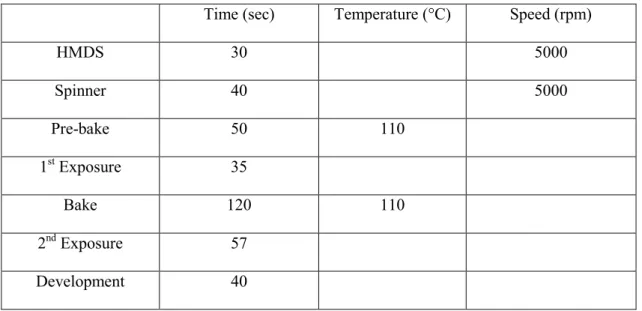
5.3.2 Mask Layout of LED and photolithography recipe ... 98
5.3.3 LED Processing Flow of LED wafer ... 100
5.4 Photonic Crystal Characterization and Fabrication ... 105
5.4.1 FIB Trials ... 105
3
5.4.3 PC fabrication characterization by E-beam lithography ... 108
5.5 Characterization Parameters ... 111
5.5.1 PMMA thickness and development ... 111
5.5.2 Exposure Parameters ... 112
5.5.3 Beam current ... 113
5.5.4 Beam energy ... 114
5.6 Characterization and fabrication of photonic crystals ... 114
5.6.1 PMMA Thickness ... 114
5.6.2 Eroding of PMMA under RIE Etching ... 115
5.6.3 Choosing Sacrificial Layer ... 117
5.6.4 Dose Characterization ... 120
5.7 Photonic Crystal Fabrication embedded in InGaN/GaN MQW LED ... 140
6. Measurement and Simulations ... 144
6.1 Introduction and measurements ... 144
6.1.1 Refractive Index Measurement ... 145
6.1.2 Absorption and Transmission Curves ... 146
6.1.3 I-V Measurements ... 147
6.1.4 Electro-luminescence spectra ... 149
6.1.5 Optical Power Measurements ... 150
6.1.6 CCD Camera Snapshots ... 153
6.2 Simulations ... 154
6.2.1 Band Structures and Band Gaps ... 155
6.2.2 2-D integral method simulations ... 161
6.2.3 FDTD Simulations ... 167
6.3 Comparison of simulations and measurements ... 189
7. Conclusion ... 191
4
8.1 2D FDTD Simulation Lumerical Scripts ... 192
8.1.1 Pre-processing ... 192
8.1.2 Post-processing ... 195
8.1.3 Finalizing ... 198
8.2 2D Integral Method Simulation Matlab Codes ... 203
8.2.1 Pre-processing ... 203
8.2.2 Post-processing ... 207
8.2.3 Finalizing and Plotting ... 209
8.3 3D FDTD Simulation Lumerical Scripts ... 210
8.3.1 Square PC lattice ... 210
8.3.2 Triangular PC Lattice ... 213
8.4 Far Field Pattern Calculations Lumerical Scripts ... 217
8.5 Power Calculations ... 218
8.6 3D FDTD Simulation Fullwave Matlab Codes ... 219
5
List of Figures
Figure 2.1 Electromagnetic spectrum and visible range ... 16
Figure 2.2 Direct and indirect band gap materials ... 17
Figure 2.3 LED-1 InGaN/GaN MQW wafers grown by collaboration with UCSB, emission wavelength 390 nm ... 22
Figure 2.4 LED-2 InGaN/GaN MQW wafers grown by collaboration with UCSB,emission wavelength 410 nm ... 22
Figure 2.5 Lattice constant vs. Band gap of wurtzite III-Nitrides ... 24
Figure 2.6 Temperature dependence on GaN lattice parameters. a) “a” side b) “c” side. (Adapted from ref. [40]) ... 26
Figure 2.7 Temperature dependence on thermal expansion coefficients of GaN grown on a) “a” plane b) “c” plane. (Adapted from ref. [40]) ... 26
Figure 3.1 p-n homojunction with no bias ... 36
Figure 3.2 p-n homojunction with forward bias ... 37
Figure 3.3 p-n junction with hetero-structure under forward bias ... 37
Figure 3.4 Discrete energy levels in quantum well region ... 41
Figure 3.5 Bowing parameter with respect to Indium molar fraction (ref. [69]) ... 41
Figure 3.6 Electro-luminescence spectra LED which emits at wavelength of 390 nm ... 43
Figure 3.7 Electro-luminescence spectra LED which emits at wavelength of 410 nm ... 43
Figure 3.8 Separation of electron-hole functions under forward bias. a. No bias. b. Forward bias ... 45
Figure 3.9 Layer structure of LED wafers grown in UCSB a. 390 nm LED b. 410 nm LED . 47 Figure 3.10 Extracted light from InGaN/GaN LED without epoxy, extraction efficieny is 3.2% ... 50
Figure 3.11 Extracted light from InGaN/GaN LED with epoxy, extraction efficiency is 3.6% ... 51 Figure 4.1 Natural Photonic Crystals. a) Green opal which reflects light at λ=560nm, with
periodic lattice constant d=420nm (ref. [95]). b) Red opal which reflect light at λ=680nm, with periodic lattice constant d=490nm (ref. [95]). c) Morpho rhetenor butterfly and the periodic structure inside its wings which creates the
6 unique color (ref. [96]). d) Peacock feather and its nano-structure with different
lattice constants which gives feather diversified colors [97]. ... 56
Figure 4.2 Types of Photonic Crystals ... 57
Figure 4.3 2D PC formed by triangular air lattices in a dielectric material ... 58
Figure 4.4 1D Photonic Crystal Structure with lattice constant “a” ... 63
Figure 4.5 Electric field and energy density of dielectric band ... 65
Figure 4.6 Bragg Condition in order to have constructive interference ... 66
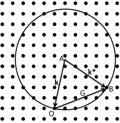
Figure 4.7 Bragg Reflection in k-space showing in Ewald Construction Circle ... 69
Figure 4.8 Two dimensional PC structure with square lattice ... 70
Figure 4.9 Square PC lattice, with lattice constant “a” and lattice radius “r” ... 70
Figure 4.10 First Brillouin zone and Irreducible Brillouin zone for square lattice ... 71
Figure 4.11 2D triangular PC lattice ... 72
Figure 4.12 First Brillouin zone and edges of irreducible Brillouin zone for triangular lattice ... 72
Figure 4.13 Light is totally reflected from the GaN-air interface for angles higher than critical angle ... 75
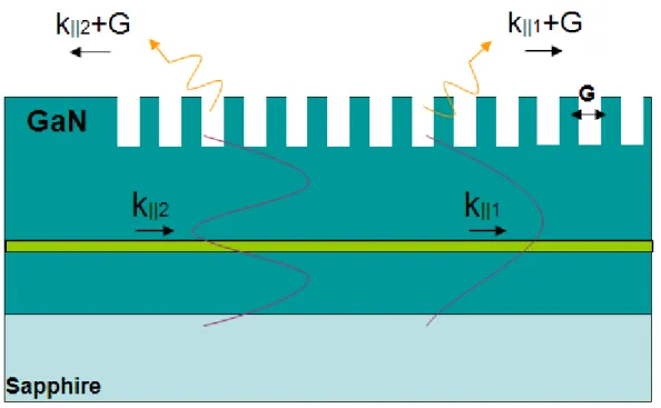
Figure 4.14 Schematic of the PC Bragg diffraction of guided modes in GaN ... 79
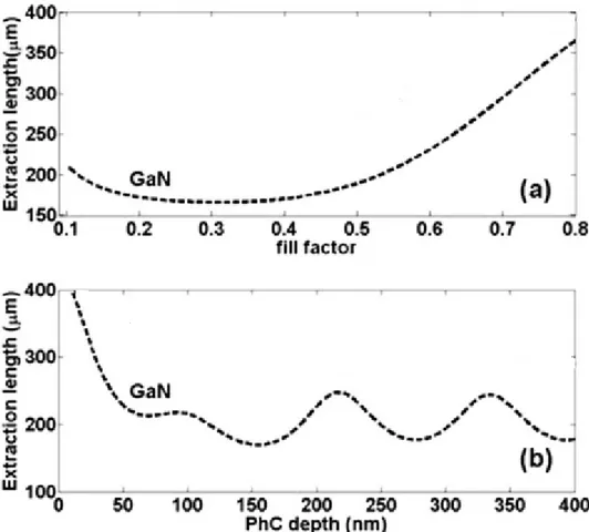
Figure 4.15 PC extraction length with respect to fill factor and PC depth for TE9 mode (79) 84 Figure 4.16 Photonic Band Gap Diagram for TE and TM modes for triangular lattice hole PC structure in GaN with r/a = 0.5 ... 85
Figure 5.1 Schematic of RIE system ... 88
Figure 5.2 Nickel as etching mask ... 90
Figure 5.3 Chromium as etch mask ... 90
Figure 5.4 5214E photo-resist as etchant mask ... 91
Figure 5.5 Etching starting point: 8 ubar, 200 W, 20 sccm ... 92
Figure 5.6 At max power of 240 W ... 92
Figure 5.7 100 W power ... 93
Figure 5.8 Max pressure ... 94
Figure 5.9 Optimum etching parameters, 1 ubar, 100 W, 30 sccm ... 95
Figure 5.10 Photolithography LED mask ... 99
Figure 5.11 Snapshots from fully processed LEDs ... 105
Figure 5.12 Dwell time vs. PC depth during FIB PC patterning ... 106
Figure 5.13 PC patterned areas by FIB system using 30 kV gallium ions ... 107
7
Figure 5.15 Final PC structure patterned by e-beam lithography system, stitching error ... 110
Figure 5.16 AFM pictures of PMMA resist on GaN a. 3D image of PMMA resist b. Line profile of the PMMA resist ... 115
Figure 5.17 Damaged PC structures because of eroded PMMA ... 116
Figure 5.18 Re-exposed PMMA under RIE etch ... 117
Figure 5.19 Over re-exposure causes all PC patterns to be washed off ... 118
Figure 5.20 Chromium sacrificial etching mask after PMMA removal ... 118
Figure 5.21 Chromium mask layer after RIE etching ... 119
Figure 5.22 SiO2 used as sacrificial mask layer ... 120
Figure 5.23GaN-SiO2- PMMA sample after PMMA develop. ... 123
Figure 5.24 RIE etch after e-beam dot dose ... 124
Figure 5.25 RIE etched sample after dot-dose exposure with de-focusing ... 124
Figure 5.26 AFM image of de-focused dot dose sample a. 3D image b. Line profile ... 125
Figure 5.27 E-beam circular dose writing scheme ... 126
Figure 5.28 RIE etched patterns after circular dose e-beam exposure using dose matrix ... 128
Figure 5.29 AFM of sample patterned with circular dose e-beam lithography ... 129
Figure 5.30 Resultant patterns after RIE etched area dose mode samples by using octagonal shape with beam current used of a. 0.22 nA b. 0.45 nA ... 130
Figure 5.31 PC structure produced by octagonal shaped soft mask, optimum exposure parameters ... 131
Figure 5.32 Sample patterned with rectangular mode, 1.5 turn de-focusing, 0.22 nA ... 132
Figure 5.33 Sample patterned with rectangular mode, ¾ turn de-focusing, 0.45 nA ... 133
Figure 5.34 Sample patterned with rectangular mode, ½ turn de-focusing, 0.45 nA ... 133
Figure 5.35 AFM picture of rectangular PC structure, 52 uAs/cm2 beam clearing dose ... 135
Figure 5.36 RIE lag effect. a. Etching in larger structures b. Etching in smaller structures .. 136
Figure 5.37 Rectangular shape, triangular PC lattice, after PMMA development ... 137
Figure 5.38 AFM picture of triangular PC lattice ... 138
Figure 5.39 AFM pictures of triangular PC lattice type a. 3D image b. Line profile ... 139
Figure 5.40 Representative AFM images of fabricated PC structures a. 3D image b. Line profile ... 142
Figure 5.41 Representative AFM images of fabricated PC structures a. 3D image b. Line profile ... 143
Figure 6.1 Inhomogenous current spreading because of high contact resistivity ... 145
8
Figure 6.3 Absorption curve of LED-1 wafer ... 146
Figure 6.4 Transmission curve of LED-1 wafer ... 146
Figure 6.5 I-V characteristics of n to n layer ... 148
Figure 6.6 I-V characteristics of p to p layer ... 148
Figure 6.7 I-V characteristics of an LED chip processed in this thesis work ... 149
Figure 6.8 I-V Characteristics of PC/NoPC LED chips ... 150
Figure 6.9 Electro-luminescence characteristic of 390 nm LED without PC structure ... 151
Figure 6.10 Electro-luminescence characteristic of 410 nm LED without PC structure ... 151
Figure 6.11 Electro-luminescence characteristic LED with PC structure, peak is at 387 nm 152 Figure 6.12 Optical power characteristics of LEDs with and without PC structures ... 152
Figure 6.13 a. CCD image of triangular PC lattice captured in black&white mode b. Intensity plot along the black line ... 153
Figure 6.14 Some other PC patterned LED devices under forward bias ... 154
Figure 6.15 TM Band Gap Edges for different filling ratios in square PC lattice ... 156
Figure 6.16 TE Band Gap Edges for different filling ratios in triangular PC lattice ... 157
Figure 6.17 TE band gap ratio with respect to filling factor for triangular hole lattice ... 157
Figure 6.18TM Band Gap Edges for different filling ratios in triangular PC lattice ... 158
Figure 6.19 TE-TM band diagram of square hole PC structure with filling ratio of 0.2 ... 160
Figure 6.20 TE-TM band diagram of triangular hole PC structure with filling ratio of 0.23 160 Figure 6.21 PC lattice borders used in 2D integral method simulations ... 161
Figure 6.22 2D integral method simulation using rectangular PC border ... 163
Figure 6.23 2D integral method simulation including PC design parameters of PC depth, filling ratio, PC period ... 164
Figure 6.24 d/a ratio vs. enhancement factor for PC structure a=520 nm, t=90 nm ... 165
Figure 6.25 Extraction enhancement ratio of rectangular PC border to sinusoidal PC border ... 166
Figure 6.26 Transmission vs. incident angle plot for PC structure with rectangular border . 168 Figure 6.27 Transmission vs. incident angle plot for PC structure with sinusoidal border ... 168
Figure 6.28 Transmission vs. incident angle plot for structure without PC ... 169
Figure 6.29 Yee’s Cell for FDTD method ... 169
Figure 6.30 2D simulation region used in thesis work ... 174
Figure 6.31 Different dipole positions along PC period ... 175
Figure 6.32 Far-field pattern of 2D PC simulation ... 175
9
Figure 6.34 System with PC structure ... 176
Figure 6.35 2D PC FDTD simulation with d/a ratio of 0.5 ... 178
Figure 6.36 2D FDTD simulation with maximum enhancement at d/a ratio of about 0.6 .... 178
Figure 6.37 3D FDTD plane wave simulation for filling ratio of 0.6 ... 180
Figure 6.38 3D FDTD simulated PC LED model ... 182
Figure 6.39 Cross-section of 3D FDTD PC LED simulation model ... 182
Figure 6.40 Refractive index map of triangular PC lattice ... 186
Figure 6.41 Far field patterns of LEDs ... 186
Figure 6.42 Refractive index map of square PC lattice ... 188
10
List of Tables
Table 2.1 General properties of III Nitrides ... 27 Table 5.1 RIE GaN etch characterization parameters ... 89 Table 5.2 Etch rates and side-wall angles ... 96 Table 5.3 RIE etch recipes ... 97 Table 5.4 Details about annealing of p layer GaN ... 98 Table 5.5 Positive resist recipe ... 100 Table 5.6 Negative resist recipe ... 101 Table 5.7 P-metal evaporation ... 101 Table 5.8 N-metal deposition ... 102 Table 5.9 Pad metal deposition ... 102 Table 5.10 LED processing overview ... 104 Table 5.11 PMMA resist recipe ... 112 Table 5.12 SiO2 growth recipe by PECVD ... 119
Table 5.13 Oxide-1 PMMA growth conditions ... 121 Table 5.14 Oxide-2 PMMA growth conditions ... 121 Table 5.15 Dot dose characterization ... 122 Table 5.16 Circle dose characterization parameters ... 126 Table 5.17 Exposure parameters for octagonal shape ... 131 Table 5.18 Exposure parameters variation range for optimization ... 134 Table 5.19 Optimized e-beam exposure parameters at 5 keV ... 138 Table 5.20 Optimized exposure parameter for PC fabrication at 10kV ... 140 Table 6.1 2D integral method simulation sweeping PC design parameters ... 162 Table 6.2 2D PC FDTD Simulation parameters ... 174 Table 6.3 2D FDTD PC parameter sweeping ranges ... 177 Table 6.4 3D FDTD plane wave simulation parameters ... 180 Table 6.5 3D FDTD point dipole simulations overview ... 184
11
1. Introduction
Chapter 1
Nitride semiconductors have drawn a lot of attention for the last two decades. They can be used in high power, high frequency optoelectronics under harsh environmental conditions such as high temperature and high pressure. Their direct band gap properties and wide spectrum coverage which includes full visible range and most of ultraviolet (UV) down to 200 nm make them excellent candidates for optoelectronic devices. With the advancements in III-Nitrides growth techniques and solutions on the problems such as p type doping, III -Nitride based systems have been fabricated and commercialized including full color bright displays, illumination devices, visible-blind UV photo-detectors, high resolution laser printers, biomedical applications, high density storage devices, and defense systems.
Among III-Nitrides, gallium nitride (GaN) has gained the most attention since it has large direct band gap of 3.4 eV at room temperature while it can form compounds with other group III elements aluminum (Al) and indium (In) which have band gaps of 6.2 eV and 0.7 eV respectively. By varying the amount of elements in the compounds, AlGaN, InGaN and AlInGaN, one can reach spectrum range starting wavelength from 200 nm up to 1500 nm which covers deep UV - UV, full visible spectra and infrared (IR). Intense research on high power GaN based light emitting diodes (LEDs) has been continued for the last decade.
Light emitting diodes are based on radiative recombination of electron and hole pairs generated in the active layer of the material, which is called solid state lighting. LEDs are the ultimate sources of illumination because of their long life time, low energy consumption, high durability, resistance to mechanical effects, quick response time and high luminescence efficiency. One of the major goals of LED research is to use LEDs in general lighting.
Efficiency of traditional light bulbs is around 1% ~ 4% and efficiency of flourescents is around 15% ~ 20%. On the other hand, LEDs can have efficiencies up to 80%. Exchanging classic 100 W light bulbs that are used in houses by LEDs will save 70% of energy that is used for lighting purposes. In order to be able to use LEDs in general lighting, high intensity
12 white light with a natural color temperature should be realized by using solid state techniques. By tuning and mixing three main colors red, green and blue in proper ratios or using phosphor with highly efficient blue LEDs can enable to have white light with a natural color temperature. GaN based light emitting diodes make this dream possible by filling the gap of the blue color in the spectrum for solid state lighting technology.
In order to be able to use LEDs for general lighting, efficacy more than 200 lm/W should be achieved. Red, amber, orange and yellow LEDs that use AlGaInP chips have already better luminous efficiency than a 100 W incandescent lamp. Higher than 100 lm/W efficiency has been achieved by using these chips. On the other hand, extraction efficiencies of GaN based green and blue LEDs are not high enough. Considering that human eye responsivity is also very low for blue color, GaN based LEDs which illuminates in the wavelength of blue should have much higher extraction efficiencies.
Although internal quantum efficiency of these blue LEDs are around 90%, external quantum efficiency drops to about 10-12%. Main reason for low extraction efficiency for GaN based LEDs is total internal reflection. Most of the light emitted from active layer of these devices cannot be used. Light which cannot get out from the device is eventually absorbed by defects and quantum wells which also cause extra-heat that is detrimental for working life of LED. Because of the high refractive index contrast between GaN (n=2.7) and outer space (n=1), light coming to the air-GaN interface reflects totally back for incident angles higher than critical angle. Critical angle for GaN is around 22°-24°. From top surface of the GaN based LED without any encapsulation, ratio of emitted light to the generated light in active layer of the device is around 1/4n2 4%. Some of other issues about low extraction efficiency are ≈ reflection from metal contacts, substrate absorption, absorption of carriers by GaN defects, impurities and InGaN/GaN quantum well layer.
Main objective of this thesis is to increase low extraction efficiency of light from GaN based LEDs. In order to increase the light output from GaN based LED, either internal quantum efficiency or extraction efficiency should be increased. Internal quantum efficiency is related to quality of the crystal structure of the material and can only be altered during growth of the material. However, it is already close to unity.
On the other hand, extraction efficiency is mostly related to the geometry of the device. By designing proper surface geometry, most of the light trapped in the high refractive index medium because of total internal reflection can escape the structure.
13 Several methods have been tried out in order to enhance light output by enlarging the light escape cone geometrically such as surface texturing [1], modifying spontaneous emission by resonant micro-cavity [2], surface plasmons [3], incorporating 2D photonic crystals [4][5][6][7]. In this thesis, photonic crystals are studied in depth in order to increase the intensity of the light that comes out of the LED. In the literature, an average of intensity increase of 1.5~2.1 times by using 2D photonic crystal (PC) structures has been reported [8]. PC increases extraction efficiency by diffracting guided modes in the material to air. Light propagating in the material with an incident angle higher than critical angle is trapped in the dielectric material. By using PC structures, these in-plane wave-vectors are folded into leaky modes so that originally guided light in the GaN material couples out into air. In order diffraction condition to be satisfied and higher number of modes to be extracted from 2D PC structure, parameters such as wavelength, mode angle, PC depth, filling factor and lattice constant should be designed carefully. Higher extraction efficiencies on LEDs have been achieved by using rather larger lattice constants [9]. The a/λ interval where most extraction efficiency achieved is stated to be between from a/λ =1 to a/λ =2 [10]. This result shows that Bragg scattering has more influence on extraction efficiency than that of band-gap approach and/or Purcell effect. Therefore, design of the PC structure is based on Bragg condition in this thesis.
In the second chapter, information about background of GaN, growth techniques, material properties, and layer structure of LED wafer processed in this thesis work are given. Third chapter is about light emitting diodes and InGaN/GaN multi quantum well (MQW) structures. Development history of LEDs and progress in InGaN/GaN and GaN based LEDs, device principles and PC LEDs are discussed. In the fourth chapter, general information about photonic crystals is given. Theoretical background about Maxwell’s equations, photonic band gap formation and fundamentals of Bragg scattering are argued. Fifth chapter comes with the details about characterization and fabrication of GaN material and PC structure. In this chapter, GaN material etching characterization, LED wafer processing steps and electron beam lithography (e-beam) based PC fabrication issues are explained comprehensively. In the sixth chapter, measurements about LED device and fabricated PC structures are shown. Technique and results of the simulations regarding extraction efficiency enhancement of GaN based LED with embedded PC structures are stated. Comparison of simulations and measurements are discussed. In seventh chapter, thesis work is concluded. At the end of the chapters, one can find references used in the thesis and appendix. In appendix, scripts and
14 codes are stated which are used and written for simulation pre-processing and post-processing.
15
2. Gallium Nitride & Material Properties
Chapter 2
2.1 Introduction
III-Nitrides are important semiconductors because of their direct band gap properties and wide spectrum coverage (full visible range and most of UV down to 200 nm). They can be used in high power, high frequency optoelectronics under harsh environmental conditions such as high temperature and high pressure. GaN is superior for having high breakdown field and high electron velocity. Since it is chemically inert, GaN is an excellent candidate for opto-electronic devices which works under harsh chemical environment.
III -Nitride based systems have been fabricated and commercialized so far including full color bright displays, illumination devices, visible-blind UV photodetectors, high resolution laser printers, biomedical applications, high density storage devices, defense systems.
Among III-Ns, GaN has gained the most attention since it has large direct bandgap of 3.4 eV at room temperature while it can form compounds with other group III elements aluminum and indium which have bandgaps of 6.2 eV and 0.7 eV respectively. By varying the amount of elements in the compounds, AlGaN, InGaN and AlInGaN, one can reach spectrum range starting wavelength from 200 nm upto 1500 nm which covers UV-deep UV, visible spectra and IR.
2.2 Direct & Indirect Band Gap Structures
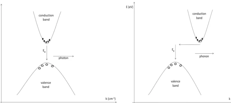
Structure of band gaps of materials characterize the optical properties of the material. Momentum difference of bands are important especially for the materials to be used in opto-electronics. Accoring to wave-vectors of maxima and minima of bands, materials are classified in two groups as direct band gap materials and indirect band gap materials.
16
Figure 2.1 Electromagnetic spectrum and visible range
In a direct band gap material, minimum of conduction band and maximum of valence band of the material have the same wave-vector k=0 as seen in figure. On the other hand, in an indirect band
gap material, those minima and maxima have not same wave-vectors, but there is a considerable variance among them.
When an electron changes its energy state, both momentum and energy of electron must be conserved. For direct band gap recombinations, since wave vector does not change significantly, most of the energy goes out in form of photons. However, since there is large difference between wave-vectors of conduction and valence band states for indirect band gap materials, momentum transfer is also introduced to the system which is achieved by vibrations of atoms, which is called phonons. Indirect band gap materials usually cannot emit photons since most of the energy is given out by phonons.
2.3 III Nitrides Background
First AlN and InN was syntehsized in 1907 and 1910 by Fichter et al and Schröter et al respectively [11][12]. In 1928, first AlN is synthesised by Tiede et. al from metalic aluminum [13]. Johnson et. al synthesised first GaN by reaction of Ga with ammonia in 1932 [14] while Juza and Hahn synthesized InN from InF6(NH4) in 1938 [ ]. After a period of 30 years, we 15
17 come to 1969, when first single crystalline GaN was grown by chemical vapor deposition method (HVPE)
Figure 2.2 Direct and indirect band gap materials
with good electrical and optical properties by Maruska and Tiejen at RCA Laboratories [16]. Afterwards, Pankove et. al demonstrated first GaN LED which was fabricated with meta-insulator-semiconductor structure in 1971[17]. In the same year, Dingle et. al showed stimulated emission is possible from optically pumped GaN needles [18]. Early 1970s is also the time of a breakthrough in growth methods since MOCVD and MBE techniques were developed in 1971 and 1974 [19] [20].
However, research groups working in the field of GaN faced with some major problems like lack of p-type doping and proper substrate. These problems caused interest of most of the groups to change. Only a few groups remained which continued to work on GaN. One of them which had been headed by Yoshida used AlN buffer layer to improve the epitaxial quality of GaN film on sapphire substrate in 1983. Finally, in 1986, Akasaki’s research group succeeded to grow high quality single crystal GaN films on sapphire which are free from surface cracks by using AlN buffer layer [21][22]. This was the first two step growth method. They grew GaN on sapphire heteroepitaxially first using a thin low temperature growth nucleation layer of AlN or GaN. Afterwards, high temperature epitaxial growth of GaN was carried out. High temperature growth on nucleation layer makes it possible GaN crystal to
18 grow not from the substrate but from the islands formed. Since this two-step procedure reduces impurity concentration and increases electron mobility, it has become a common method used for growing GaN.
In 1991, same group showed that it is possible to make p-type from Mg-doped GaN by using low-energy electron beam irradiation (LEEBI) [23]. S. Nakamura discovered just after Akasaki’s p-type success that the same p-type GaN can be made by annealing Mg doped GaN under N2 environment [ ]. 24
Until then, as the two main problems in the field of GaN were eliminated, high density researches have been ongoing since 1990s by several groups throughout the world.
2.4 Growth of GaN
GaN is grown epitaxially since epitaxy obtains high crystalline structure which is needed for opto-electronic devices to work. Since there is no common bulk GaN substrate, GaN is grown on most similar compound that can be found in which growth is called heteroepitaxial growth. Bulk crystal growth techniques generally rely on solid-liquid phase equilibrium for the substrate material. Since melting point of GaN is very high, as the temperature is increased, compound starts to decompose and III-V elements start to melt. In order to prevent the decomposition, extra huge pressure of nitrogen is needed, which is not practical. Therefore, no bulk GaN crystal is commonly commercialized.
As choosing proper substrate for GaN, there are number of important criteria. First of all, substrate should be strong at temperatures higher than 1000 C° since growth temperature of GaN is around this temperature. Also thermal mismatch between substrate and GaN should be small in order to prevent crack generation while the film cools down to room temperature from high growth temperature. In addition, crystal structure of the substrate should be close to that of GaN to prevent cracking during growth. Therefore substrate should have three or six fold symmetry for wurtzite GaN and close lattice constant to lattice constant of GaN. As GaN LEDs are to be used in high power applications, substrate should have high coefficient of thermal conductivity so that heat generated in the LED can easily radiate away.
Alumina and SiC are the most proper substrates commonly used for GaN epitaxial growth. However, there still is high lattice and thermal mismatch between the substrate and GaN film, therefore high density of defects occur in the film. Although lattice mismatch between
19 substrate and film is much lower for SiC than that for sapphire (3.4 % vs. 13 %), quality of grown film is not as expected because of surface structure of SiC. High cost and low bandgap energies are also drawbacks of SiC as a substrate. Two-inch-sapphire substrate costs about $ 200 while same size SiC is around $ 3000. For comparison, widely used Si substrate is sold for $ 15. Therefore, alumina is more frequently used.
Some of the growth techniques which are used to grow GaN are MOCVD (Metal Oxide Chemical Vapor Deposition), HVPE (Hyride Vapor Phase Epitaxy), MBE (Molecular Beam Epitaxy), hot wall epitaxy etc. Among these, MOCVD is the most commonly used system. Most of the breakthroughs about GaN material was carried out by using MOCVD (or MOVPE-Metal Organic Vapor Phase Epitaxy) system.
MOCVD was pioneered by Manasevit et. al in late 1960s [19]. Metal organic vapor phase epitaxy (MOVPE) is the same technique in literature. Growth in MOCVD is based on chemical vapor deposition. Vapor phase of precursors of required compounds are sent to surface of the substrate. Solid starts to be deposited on the substrate by chemical reactions. In MOCVD, 30nm/min growth rate is usual. Thermal – lattice mismatch effect is low. There is high background carrier concentration up to 1019 /cm3
25
in the grown film which is caused by incorporation of oxygen impurities [ ].
In this system, metal organic (MO) compounds are used in order to grow the film on the substrate. In order to carry these MO sources, which are high vapor pressure liquids, high purity H2
In order to grow GaN, MO compound precursor TMG (Trimethylgallium) and NH gas is commonly used. Wafer is heated by radio frequency (RF) heater in the quartz tube growth chamber. Substrate is placed on the SiC coated susceptor. As the substrate is heated, chemical reactions start to take place on the substrate since high temperature behaves as catalysor. As gaseous MO compounds are decomposed, GaN film is grown on the substrate. Growth rate can be judged by examining physical conditions such as substrate temperature, reactant partial pressure, gas flow etc. in the chamber during growth.
3
(Ammonia) are used. Growth takes place under high temperature up to 1000-1100C°. Among sources, although TMG can be decomposed at temperature around 600C°, NH3 requires much
higher temperature values in order to decompose effectively. Since no bulk GaN substrate is feasibly present, GaN is heteroepitaxially grown on a different substrate. Because of the lattice constant mismatch and thermal coefficient mismatch, there occurs high thermal strain during period of cooling from temperature of 1000 C° down to room temperature. Although researchers have been working on a solution in order to decrease the growth temperature such
20 as changing sources or braking N2
In order to decrease the cracking and defects caused by thermal strain, a buffer layer between GaN and sapphire is used which is grown at lower temperature. Buffer layers of AlN and GaN are reported to have improvements on the epitaxial layer quality by Akasaki et al. and Nakamura et al. [
molecules into radicals, classical MOCVD precursors seem to give highest film quality.
21][26]. These buffer layers are generally grown around at 500~750 °C which give better quality than GaN grown on sapphire at 1000 °C. Akasaki et al. showed that low temperature grown AlN is amorphous [22][27]. This amorphous layer covers the substrate uniformly. On the other hand, GaN without buffer layer has columnar nucleation which ends up with defects after critical thickness and during cooling down. That amorphous layer crystallizes when temperature is increased during GaN layer growth, which forms a great growth surface for GaN. As a result, buffer layer decreases the amount of strain between GaN and sapphire which is caused by thermal and lattice constant contrast and gives a way to less defected GaN layer.
Below is the chemical reaction that occurs on the substrate while the GaN film is being grown.
Ga(CH3)3(v) + NH3(v) GaN(s) + 3CH4(v) (2.1)
While growing AlGaN and InGaN layers, pre-cursors of trimethylaluminum (TMAl) and trimethylindium (TMIn) are used. In order to dope the film by p type and n type, cyclopentadienylmagnesium (Cp2Mg) and disilane (Si2H6) or silane (SiH4)
Other commonly used methods available for GaN growth are MBE and HVPE. In MBE, group V source Nitrogen is supplied as atomic nitrogen by using plasma. Since no ammonia is needed in this growth method, high temperature in order to break N-H bonds is not a must and therefore lower growth temperatures are possible. However, growth rate in MBE is low. In HVPE method, chlorine is used in order to transport group III materials and very high growth rates up to 100um/h can be achieved [
are used respectively.
GaN has two faces to be grown on, Ga and N faces. Ga face is the usual grown face in MOCVD since it gives better surface characteristics. N face is also possible by highly doping with Mg; however, surface quality and stability of the film is not as good as that of Ga face grown film.
21 metallic Ga which is in liquid form. As a result of chemical reaction between two compounds, a new compound GaCl in gaseous state is formed. By uisng N2 gas as carrier, GaCl is carried
into the reaction chamber where it reacts with NH3 to form GaN (solid). HCl (gas) and H2
(gas) are by-products. This method is not suitable for fabricating optoelectronic devices though since film quality is not adequate.
2.5 Structure of InGaN/GaN QW LED wafer grown by
collaboration with UCSB
LED wafers processed and patterned in this thesis were grown by collaboration with University of California Santa Barbara (UCSB). There are two different grown LED wafers. They have InGaN/GaN MQWs with 5% and 8% Indium concentration, which are called LED-1 and LED-2 respectively. Structures of LED wafers are drawn below in Figure 2.3 and Figure 2.4.
Electroluminescence and I-V curves of both wafers are stated in Chapter 6. Photonic crystal patterning is done on LED-1. Therefore, in this thesis, electrical and optical properties are mostly studied on LED-1 wafer.
As seen from structures, n type layer of LED-1 wafer is relatively thin and based on AlGaN compound. As will be stated later, metal contacts on n type AlGaN layer and thin n type doped layers show higher resistivity which end up with higher turn-on voltages. This kind of behaviour is also seen in measurements of processed LEDs in this thesis, which are shown in chapter 6.
Thin AlGaN layer with Mg doping on top of quantum wells is used in order to confine the carriers in quantum well regions. This layer is also called as electron blocking layer (EBL).
2.6 Chemical and Physical Properties of GaN
In this part, some of important properties of III nitride semiconductors are outlined. Although the properties stated mainly belongs to GaN, AlN and InN, properties for ternary compounds such as InGaN or AlGaN can be found by making interpolation between GaN and InN or GaN and AlN.
22
Figure 2.3 LED-1 InGaN/GaN MQW wafers grown by collaboration with UCSB, emission wavelength 390 nm
23
2.6.1 Band Gap of GaN and InN
Bandgap energy of GaN at room temperature is 3.39~3.43 eV. As the temperature is decreased to 1.6 K, band-gap increases to 3.503 eV [29]. Temperature dependence is formulized empirically below for T<295K as,
4 2 g
3.503 5.08 10 T(K)
E (T)
996 T(K)
−−
×
=
−
(2.2)where temperature T is in Kelvin. As seen from empirical formula, as temperature of the medium is decreased, band gap of GaN increases.
Since GaN is a direct band-gap material, absorption occurs by band to band excitation. Absorption coefficient can be expressed as below [30].
*
-
gA
h E
α
=
υ
(2.3)where hυ > Eg and A* is a function of electron and hole effective masses and inversely
proportional to the refractive index. Dielectric constant of GaN at high frequency limit is ε0 =
5.35 while low frequency limit is ε∞ = 9.5 [ ]. 31
Electronic band gap of InN was believed to be 1.8-2 eV at room temperature. However, researchers have found that high quality InN grown on GaN by MBE or MOCVD has a true bandgap around 0.8-0.9 eV and can change between 0.7 and 1 eV due to the difference in crystallinity [32][33].
2.6.2 Bonding Structure
Bond strength between Ga and N atoms are very high. Bond length of GaN is 1.94 A° at 300K with 2.24 eV of cohesive energy [34]. Bond length of InN is 2.15 A° while cohesive energy is 1.93 eV [34]. Electronegativities among group III atoms are 3.0 for Nitrogen, 1.18 for Aluminum, 1.13 for Gallium, and 0.99 for Indium. This high difference between electronegativities and high bond strength makes chemical bonds of III Nitrides and GaN very strong and stable. Therefore, GaN has high thermal stability and high hardness.
24 3,1 3,2 3,3 3,4 3,5 3,6 0 1 2 3 4 5 6 7
InN
AlN
Band gap (
eV
)
Lattice constant (Angstrom)
GaN
Figure 2.5 Lattice constant vs. Band gap of wurtzite III-Nitrides
Since bonds are strong, melting points of III nitrides are also high. Melting temperature of GaN is around 2500 C° while melting point of InN is around 1300 C°. However, decomposition temperature of GaN is much lower [35].
Thermal conductivity of GaN along c direction is 1.3 W/cmK at room temperature [36]. However, as the temperature is decrased, thermal conductivity decreases dramatically, down to 0.4 W/cmK.
2.6.3 Crystal Structure
III-Nitrides AlGaN, GaN and InGaN have covalent bondings. Because of high electronegativity of group V element Nitrogen with respect to group III elements Aluminum, Gallium and Indium, these compounds have also a strong ionic character which improves chemical stability of III-Ns.
25 Each atom in those compunds has four tetrahedral bonds. Since none of III-Nitrides have central symmetry for specific growth planes (no center of inversion), III-Nitrides induce strong polarization in the material.
III-Nitrides can be crystallized in three geometries, which are wurtzite, zinc blend and rock salt. Under room temperature and normal pressure, wurtzite structure is the thermodynamically stable one. For higher perssures, III-Ns crytallize in rock salt structure. Zinc blend structure has a metastable thermodynamics and can be achieved by epitaxial growth.
Wurtzite structure, which is the most common for III-Nitrides, is in P63mc(C46v
37
) space group and formed by two close packed hexagonal lattices that are shifted along c axis by an amount of 5/8c. Stacking order goes as AaBbAaBb [ ]. While c-plane {0001} of GaN is polar because of none central symmetry, other two main planes a-plane {112¯0} and m-plane {11¯00} are nonpolar.
Lattice constants of wurtzite GaN are 3.188 A° for “a” side, 5.186 A° for “c” side at 294 K [38]. Lattice constants of wutzite InN are a=3.53-3.548 A°, c= 5.69-5.76 A° [39]. For wurtzite AlN lattice constants are “a” = 3.11 A°, “c” = 4.98 A°.
Lattice constants are dependent on temperature. In general, as the temperature increases, lattice constant also increases. Temperature dependence of lattice constants for “a” and “c” sides, and thermal coefficients of GaN grown on “a” and “c” planes is shown in the figures below [35].
Below in the Table 2.1, general properties of III Nitrides can be found.
2.7 Impurities in GaN
Impurities are foreign materials that are incorporated in GaN thin film. Parts of these impurities are unintentional which diffuses from the sources and the environment and should be decreased to minimum. Those which are intentional impurities are placed in the film on purpose, in order to control optical and electrical properties of the film.
26
Figure 2.6 Temperature dependence on GaN lattice parameters. a) “a” side b) “c” side. (Adapted from ref. [40])
Figure 2.7 Temperature dependence on thermal expansion coefficients of GaN grown on a) “a” plane b) “c” plane. (Adapted from ref. [40])
27 Property GaN wurtzite AlN wurtzite InN wurtzite Sapphire rhombohedral SiC 6H-wurtzite Lattice constant a (A°) 3.188 3.11 3.54 4.75 3.08 Lattice constant c (A°) 5.186 4.98 5.7 12.99 15.12 Density (g/cm3) 6.1 3.25 6.88
Band gap energy
300 K (eV) 3.39~3.43 6.2 0.7~1 6.2 Bond length (A°) 1.94 1.89 2.15 Melting point (K) 1500 2500 1200 Thermal expansion coefficient a direction (10-6 K-1 4.3 ) 5.27 5.6 7.5 Thermal expansion coefficient c direction (10-6 K-1 4 ) 4.15 3.8 8.5 Cohesive energy (eV) 2.24 2.88 1.93 Dielectric constant 8.9 8.5 15.3 Thermal conductivity 1.3 2 0.5
28 Among unintentional dopants, carbon and oxygen are the most common ones that are encountered in grown GaN thin film. Carbon mainly comes from metal organic sources and also from the susceptor in the MOCVD chamber. Chemistry of the source material is distinctive for the level of carbon contamination since decomposition mechanisms of sources differ from each. High level of carbon incorporation causes n-type material to compensate. Oxygen is another impurity that is diffused into film unintentionally. It occupies N site of GaN and acts as a donor. Oxygen impurity is based on contaminant in reactor or source gases. It is the main reason of high level electron concentration in unintentionally doped GaN.
Main intentional dopants are Mg and Si which are used in order to have p and n type GaN respectively.
2.7.1 Doping
Doping is crucial for optoelectronic semiconductor devices since optical and electrical properties of materials are greatly altered by different doping types and levels. Undoped GaN film generally shows n-type property which as described as unintentioanlly n-type. Reason for this unintentional n-type property is attributed to N vacancies [16] and/or residual impurities such as Si which replaces Ga, and O which replaces N [41].
There are two kinds of intentional doping types, n type doping and p type doping. In n type doping, related part of the semiconductor material is filled with excess free electrons that can move relatively free. As contrast, in p type doping, free positive charge carriers (holes) are introduced into the material. For GaN, n type doping is realized by SiH4 or Si2H6, while p
type doping is done by using Cp2
P type doping had been a major problem which decelerated and even stopped the progress of GaN research until the beginning of 1990s. Although studies on Mg doping had been ongoing since 1970s, no p type property was observed till 1989, which was achieved by using low electron energy beam irradiation (LEEBI) method on compensated Mg-doped GaN [
Mg precursors.
23]. Afterwards, other post-process methods, such as annealing the Mg doped GaN under N2-O2
24
environment by Nakamura, were used [ ]. Main reason of p type doping problem was the passivation of Mg dopants by hydrogen and forming Mg-H complexes during the growth of GaN. If the p doping of the GaN is not adequate, or there is a problem in activation of Mg,
29 parasitic resistance throughout the device occurs and high turn-on voltage values are seen in LEDs which is one probable cause of high working voltage of LEDs processed in this thesis. Magnesium activation process is reversible. If the wafer is annealed under Hydrogen environment or processed under high temperature in an environment containing H2, activated
Mg dopants become passivated again by forming Mg-H complexes. Therefore, processes like plasma enhanced chemical vapor deposition (PECVD) and reactive ion etching (RIE) with using H2 gases (SiH4, CHF3
Silicon is used to make n type GaN material during growth by using SiH
) may de-activate Mg and decrease the level of p type doping which will end up with high internal resistance and low current spreading.
4 or Si2H6
precursors. High levels of electron concentration as much as 6x1019 cm-3
42
can be achieved [ ]. However, as the concentration of Si doping is increased, so the stress induced on the film, which results degradation of the film quality by formation of V shaped cracks [42]. Hole concentration is lower than electron concentration in GaN because Mg acceptor level for GaN is 170 meV higher above valance band which is much larger than thermal energy at room temperature. This causes resistivity of p layer is much higher than that of n layer GaN. In order to decrease n layer resistivity more, rapid thermal annealing method is used for Ti/Al metallization at around 700~900 °C [43].
2.7.2 Defects in GaN
GaN based materials can be used in a wide range of spectra from near infrared to deep UV under high power, high temperature conditions. However, high density of defects in GaN material prevents GaN and GaN based compounds to be used in full performance for opto-electronic applications.
Mostly faced structural defects in GaN are stacking faults and dislocations.
Stacking faults are 2D defects and caused by crystal structure change from wurtzite to zinc blend. Free energy between these crystal structures is very small [44]. These defects are parallel to c growth direction which extends to surface.
There are also 1D point defects in GaN which plays crucial role in terms of optical and electrical properties. 1D defects can be intrinsic, Ga and/or N vacancy, or extrinsic caused by impurities such as C, H, O, Mg, Si etc. 1D defects are centers for electron traps, electron-hole recombinations, scatterings and also act as donors and acceptors.
30 Threading dislocations form at growth interface because of the strain caused by lattice mismatch between substrate material and film. Since no large enough GaN substrate with single crystal exists for homo-epitaxy, GaN based semiconductor materials are grown on foreign substrates which have thermal constant and lattice constant not the same but close to that of GaN. Sapphire is the most commonly used substrate for growing GaN based films. Lattice mismatch between the sapphire substrate and GaN and AlN nucleation layer is higher than 13 %. High mismatch causes film to be stressed and lead to island growth of GaN and AlN on sapphire. GaN crystals continue to grow not from the substrate but from these islands formed at high temperature. Dislocations are formed by coalescing of these initial islands [45]. The result is a high amount of grains and grain boundaries.
GaN materials grown on sapphire substrate have dislocation density of about 108-1010 /cm2
Pure edge dislocation is the most dominant dislocation type seen in GaN material and has an increasing percentage from 40% to 70% for the film thickness from 1um to 5um [
. There two main type of dislocations seen in GaN thin films. These are edge and screw dislocations. Edge dislocations are formed by an extra plane that is inserted in the crystal lattice structure while screw dislocations have additional lattice which is seen as a lattice step on the outer surface of the crystal. Dislocations are formed mainly during epitaxial growth.
45]. Pure screw dislocation has 10 % percentage for MOCVD grown GaN materials [46]. Others are just mixed dislocations that of edge and screw.
Screw dislocations stay in the growth direction and extend to the surface such as stacking faults.
During GaN growth, up to first 2 um, both edge and screw dislocation density is high. However, since edge dislocations terminate around this level of growth, film grown on this 2um GaN will have lower density of edge dislocation but still large amount of screw dislocations. Therefore, first 2um layer of GaN is also said to be template layer and GaN films are grown thick [47], generally more than 5 microns in order to have good surface quality. Dislocations have negative effects on the performance of the devices [48], such as serving as scattering centers for carriers, non-radiative recombination centers, charge scatter centers, deep level traps for minority carriers and current leakage paths [48] [49]. For LED case, since refractive index difference is high between GaN and air, most of the light generated in the active layer reflects back into the material. Majority of this reflected light is absorbed by defects and active layer.
31 With the efforts to decrease the dislocation density, new growth methods such as lateral epitaxial overgrowth (LEO), facet controlled LEO, high temperature annealing with over-pressurized N2 [ ][51] are applied resulting in threading dislocation density range of 1050 5 –
106 /cm2
2.7.3 Defect related Illumination Peaks seen on GaN
.Main aim is to develop a 2” bulk GaN substrate so that stress formed between the substrate and film can be decreased tremendously which results in less threading dislocations.
Beside main illumination at bandgap energy of 3.4 eV, there are also seen peaks at energy levels of 1.8 eV, 2.2-2.3 eV and 2.8-2.9 eV, which are called as red, yellow and blue illumination peaks. Main reason of these secondary peaks is because film quality is not very well for GaN [52]. There have been different thoughts on the cause of these illuminations whether they are caused by impurities and residuals (carbon, silicon, magnesium) and impurity based trap centers [53][17][52], grain boundaries-dislocations [54], intrinsic point defects such as Ga or N vacancies [55]. Most of the researchers now lean to side of point defects (Ga vacancy) especially for yellow illumination case.
The yellow luminescence has been observed in both bulk crystal and also epitaxially growth thin films, which are undoped and doped, by several methods such as MOCVD, MBE, HVPE. While intenisty of yellow luminescence can vary, good quality crytals show almost no yellow illumination [55].
Mechanism for yellow illumination is explained to be a transition from a shallow donor to a deep acceptor [56].
2.8 Polarization Issues and Quantum Confined Stark Effect
(QCSE)
Wurtzite structured III-Nitrides posses different optical and electrical properties from other semi-conductors because of symmetry issues. Wurtzite structures show central symmetry with respect to m- and a- planes but not for c- plane. This lack of central symmetry causes strong spontaneous polarization fields in the material.
32 There also occur piezoelectric fields in the material because of lattice mismatch. During the film growth, layers of the film are stressed in case there is difference between lattice constants of the subsequent films (e.g. InGaN on GaN). Strain formed along the layers of the film induces piezoelectric polarization field. Spontaneous and peizoelectric fields in the material add up to large internal electric fields.
As a result of these polarization effects, structures of InGaN-GaN quantum wells are distorted and electron and hole wave functions get separated. Reduced overlap between electron and hole functions reduces recombination rates. Amount of tunneling of carriers through quantum well regions increases which decrease carrier life time and causes absorption spectra to broaden [57].
In-field polarization results with a valence band splitting, red-shifting of emission wavelength, polarized emission from active layer, decrease in intensity of light output and different refractive indices between direction parallel and vertical to the growth axis [58]. In order to decrease QCSE, thin quantum well regions are required. Details about QCSE can be found in chapter 3.
33
3. Light Emitting Diodes and InGaN/GaN Multi
Quantum Wells
Chapter 3
3.1 Introduction
Light emitting diodes are based on radiative recombination of electron and hole pairs generated in the active layer of the material, which is called solid state lighting. LEDs are the ultimate sources of illumination because of their long life time, low energy consumption, high durability, resistance to mechanical effects, quick response time and high luminescence efficiency. One of the major goals of LED research is to use LEDs in general lighting. Efficiency of traditional light bulbs are around 1% ~ 4% and efficiency of flourescents are around 15% ~ 20%. On the other hand, LEDs can have efficiencies up to 80%. Exchanging classic 100 W light bulbs that are used in houses by LEDs will save 70% ~ 85% energy. By tuning and mixing three main colors properly or using phosphor with highly efficient blue LED can enable to have white light with a natural color temperature. GaN based light emitting diodes make this dream possible by filling the gap of blue color in the spectrum for solid state lighting technology. III-nitride LEDs can be used for numerous applications in illumination systems such as traffic lights, color displays, device backlighting, decorative and white light emitting diodes.
To be able to use LEDs for general lighting, efficacy more than 200 lm/W should be achieved. Main reason for low extraction efficiency for GaN based LEDs is total internal reflection. Therefore, most effort has been given to increase extraction efficiency by changing the geometry of the shape of device so that larger amount of light could escape from high refractive index material GaN.
In this chapter, mainly history of general LED development and particularly GaN based LED development, p-n junctions, effect of multi quantum well hetero-junctions and emission from